

Fairchild BSS123 service manual
BSS123
BSS123
N-Channel Logic Level Enhancement Mode Field Effect Transistor
June 2003
General Description
These N-Channel enhancement mode field effect
transistors are produced using Fairchild’s proprietary,
high cell density, DMOS technology. These products
have been designed to minimize on-state resistance
while provide rugged, reliable, and fast switching
performance.These products are particularly suited for
low voltage, low current applications such as small
servo motor control, power MOSFET gate drivers, and
other switching applications.
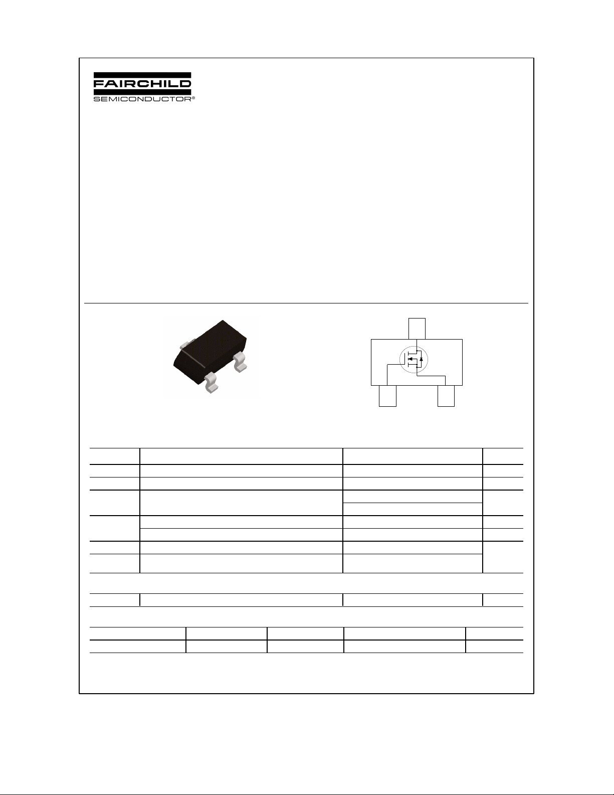
D
Features
• 0.17 A, 100 V. R
• High density cell design for extremely low R
• Rugged and Reliable
• Compact industry standard SOT-23 surface mount
package
= 6Ω @ VGS = 10 V
DS(ON)
R
= 10Ω @ VGS = 4.5 V
DS(ON)
D
DS(ON)
S
G
SOT-23
Absolute Maximum Ratings T
G
=25oC unless otherwise noted
A
Symbol Parameter Ratings Units
V
DSS
V
GSS
I
D
D
TJ, T
T
L
STG
Drain-Source Voltage 100 V
Gate-Source Voltage
Drain Current – Continuous (Note 1) 0.17 A
– Pulsed 0.68
Maximum Power Dissipation (Note 1) 0.36
Derate Above 25°C
Operating and Storage Junction Temperature Range
Maximum Lead Temperature for Soldering
Purposes, 1/16” from Case for 10 Seconds
±20
2.8
−55 to +150 °C
300
S
mW/°C
V
WP
Thermal Characteristics
R
θJA
Thermal Resistance, Junction-to-Ambient (Note 1) 350
Package Marking and Ordering Information
Device Marking Device Reel Size Tape width Quantity
SA BSS123 7’’ 8mm 3000 units
2003 Fairchild Semiconductor Corporation
°C/W
BSS123 Rev G(W)
Electrical Characteristics T
GS
BSS123
= 25°C unless otherwise noted
A
Symbol Parameter Test Conditions Min Typ Max Units
Off Characteristics
BV
DSS
∆BVDSS
∆T
J
I
DSS
I
GSS
Drain–Source Breakdown Voltage
Breakdown Voltage Temperature
VGS = 0 V, ID = 250 µA
ID = 250 µA,Referenced to 25°C
100 V
97
Coefficient
Zero Gate Voltage Drain Current VDS = 100 V, VGS = 0 V 1
VDS = 100 V,VGS = 0 V TJ = 125°C
VDS = 20 V, VGS = 0 V 10 nA
Gate–Body Leakage.
VGS = ±20 V, VDS = 0 V ±50
mV/°C
60
On Characteristics (Note 2)
V
GS(th)
∆VGS(th)
∆T
J
R
DS(on)
I
D(on)
g
FS
Gate Threshold Voltage VDS = VGS, ID = 1 mA 0.8 1.7 2 V
Gate Threshold Voltage
ID = 1 mA,Referenced to 25°C
–2.7
mV/°C
Temperature Coefficient
Static Drain–Source
On–Resistance
VGS = 10 V, ID = 0.17 A
VGS = 4.5 V, ID = 0.17 A
V
= 10 V, ID = 0.17 A, TJ = 125°C
1.2
1.3
2.2
6
10
12
On–State Drain Current VGS = 10 V, VDS = 5 V 0.68 A
Forward Transconductance VDS = 10V, ID = 0.17 A 0.08 0.8 S
Dynamic Characteristics
C
iss
C
oss
C
rss
R
G
Input Capacitance 73 pF
Output Capacitance 7 pF
Reverse Transfer Capacitance
VDS = 25 V, V
f = 1.0 MHz
GS
= 0 V,
3.4 pF
Gate Resistance VGS = 15 mV, f = 1.0 MHz 2.2
Switching Characteristics (Note 2)
t
t
t
t
Q
Q
Q
d(on)
r
d(off)
f
g
gs
gd
Turn–On Delay Time 1.7 3.4 ns
Turn–On Rise Time 9 18 ns
VDD = 30 V, ID = 0.28 A,
VGS = 10 V, R
GEN
= 6 Ω
Turn–Off Delay Time 17 31 ns
Turn–Off Fall Time
Total Gate Charge 1.8 2.5 nC
Gate–Source Charge 0.2 nC
VDS = 30 V, ID = 0.22 A,
VGS = 10 V
Gate–Drain Charge
2.4 5 ns
0.3 nC
Drain–Source Diode Characteristics and Maximum Ratings
I
S
V
SD
t
rr
Q
rr
NOTE:
1. R
θJA
the drain pins. R
Maximum Continuous Drain–Source Diode Forward Current 0.17 A
Drain–Source Diode Forward
VGS = 0 V, IS = 0.34 A(Note 2) 0.8 1.3 V
Voltage
Diode Reverse Recovery Time 11 nS
Diode Reverse Recovery Charge
is the sum of the junction-to-case and case-to-ambient thermal resistance where the case thermal reference is defined as the solder mounting surface of
is guaranteed by design while R
θJC
θCA
IF = 0.17 A,
diF/dt = 100 A/µs
is determined by the user's board design.
3 nC
µA
µA
nA
Ω
Ω
a) 350°C/W when mounted on a
minimum pad..
Scale 1 : 1 on letter size paper
2. Pulse Test: Pulse Width ≤ 300 µs, Duty Cycle ≤ 2.0%
BSS123 Rev G(W)
 Loading...