BSR17A
NPN General Purpose Amplifier
NPN General Purpose Amplifier
June 2007
C
E
B
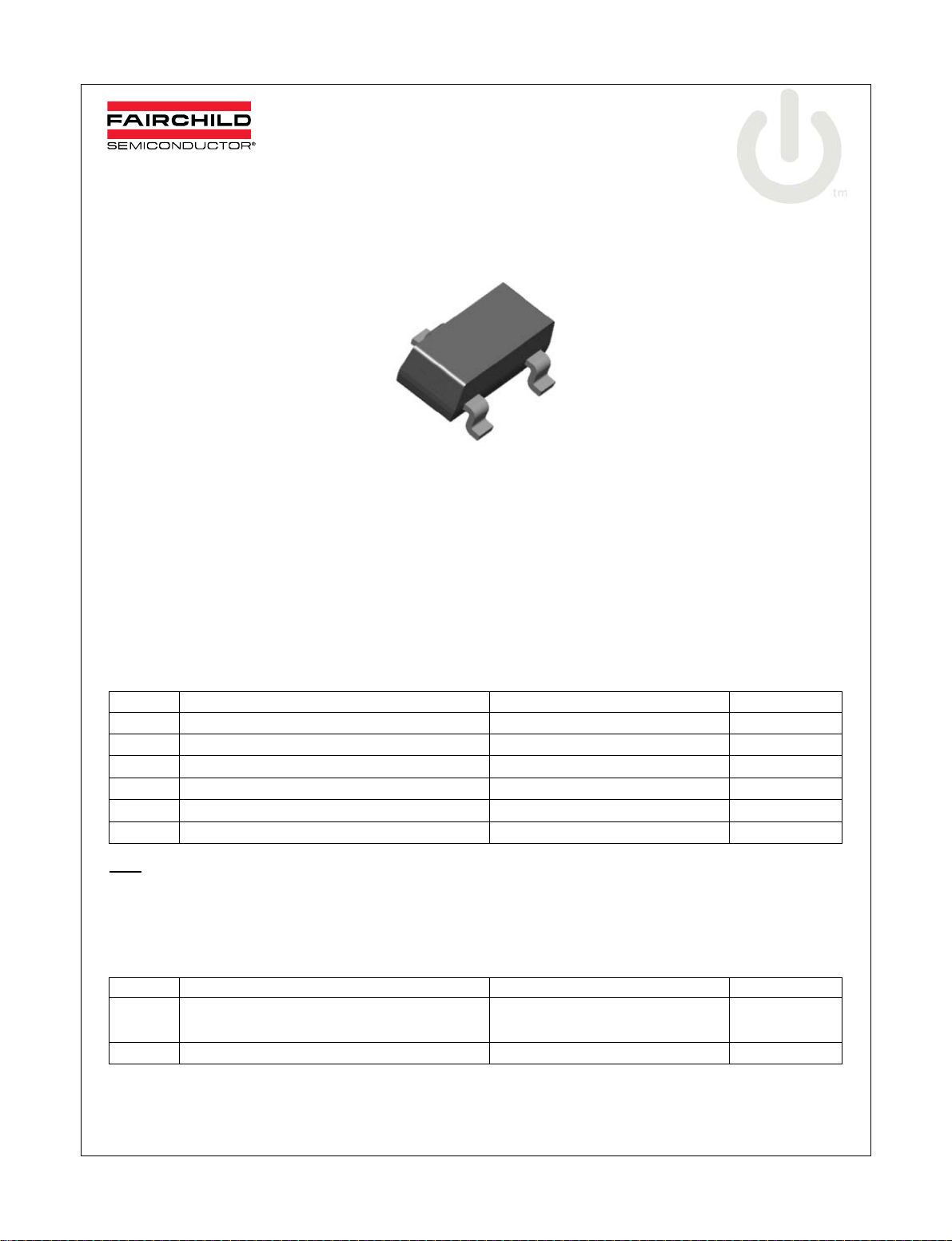
SOT-23
MARK: U92
Features
This device is designed as a general purpose amplifier and switch.
The useful dynamic range extends to 100 mA as a switch and to 100 MHz as an amplifier. Sourced from Process 23.
Absolute Maximum Ratings *T
Symbol Parameter Value Units
V
CBO
V
CEO
V
EBO
I
C
T
J
T
STG
* These ratings are limiting values above which the serviceability of any semiconductor device may be impaired.
NOTES:
1) These ratings are based on a maximum junction temperature of 150 degrees C.
2) These are steady state limits. The factory should be consulted on applications involving pulsed or low duty cycle operations.
Collector-Base Voltage 60 V
Collector-Emitter Voltage 40 V
Emitter-Base Voltage 6.0 V
Collector Current (DC) 200 mA
Junction Temperature -55 ~ +150 °C
Storage Temperature -55 ~ +150 °C
Thermal Characteristics *T
Symbol Characteristic Max Units
PD
R θ JA Thermal Resistance, Junction to Ambient 357 ℃/W
*Device mounted on FR-4 PCB 40 mm X 40 mm X 1.5 mm.
Total Device Dissipation
Derate above 25℃
= 25°C unless otherwise noted
a
= 25°C unless otherwise noted
a
350
2.8
mW
mW/℃
©2007 Fairchild Semiconductor Corporation 1 www.fairchildsemi.com
Rev. A

BSR17A NPN General Purpose Amplifier
Electrical Characteristics *T
= 25°C unless otherwise noted
a
Symbol Parameter Test Condition MIN MAX Units
Off Characteristics
V(BR)CEO Collector-Emitter Breakdown Voltage IC = 1.0 mA, IB = 0 40 V
V(BR)CBO Collector-Base Breakdown Voltage IC = 10 µA, IB = 0 60 V
V(BR)EBO Emitter-Base Breakdown Voltage IC = 10 µA, IB = 0 6.0 V
ICBO Collector-Cutoff Current VCB = 30 V, TA = 150°C 5.0 µA
ICEX Emitter-Cu to ff Current VCE = 30 V, VEB = 3.0 V 50 nA
IBEX IBEX Reverse Base Current VCE = 30 V, VEB = 3.0 V 50 nA
On Characteristics
hFE DC Current Gain IC = 0.1 mA, VCE = 1.0 V
IC = 1.0 mA, VCE = 1.0 V
IC = 10 mA, VCE = 1.0 V
IC = 50 mA, VCE = 1.0 V
IC = 100 mA, VCE = 1.0 V
VCE(sat) Collector-Emitter Saturation Voltage * IC = 10 mA, IB = 1.0 mA
IC = 50 mA, IB = 5.0 mA
VBE(sat) Emitter-Base Breakdown Voltage * IC = 10 mA, IB = 1.0 mA
IC = 50 mA, IB = 5.0 mA
40
70
100
60
30
0.65 0.85
300
0.2
0.3
0.95
Small Signal Characteristics
fT Transition Frequency IC = 20 mA, VCE = 20 V, f = 100 MHz 300 MHz
Ccb Collector-Base Capacitance VCB = 0.5 V, IE = 0, f = 1.0 MHz 4.0 pF
Ceb Emitter-Base Capacitance VEB = 0.5 V, IC = 0, f = 1.0 MHz 8.0 pF
hie Input Impedance VCE= 10 V,IC= 1.0 mA,f=1.0 kHz 1.0 10 kΩ
hfe Small-Signal Current Gain VCE= 10 V,IC= 1.0 mA,f=1.0 kHz 100 400
hoe Output Admittance VCE= 10 V,IC= 1.0 mA,f=1.0 kHz 1.0 40 µS
V
V
V
V
Switching Characteristics
td Delay Time IC = 10 mA, IB1 = 1.0 mA,VEB= 0.5 V 35 ns
tr Rise Time 4.0 pF
ts Storage Time IC = 10 mA, IBon = IBoff = 1.0 mA 200 ns
tf Fall Time 50 ns
*Pulse Test: Pulse Width 300 s, Duty Cycle 2.0 %
Spice Model
NPN (Is=6.734f Xti=3 Eg=1.11 Vaf=74.03 Bf=416.4 Ne=1.259 Ise=6.734 Ikf=66.78m Xtb=1.5 Br=.7371 Nc=2
Isc=0 Ikr=0 Rc=1 Cjc=3.638p Mjc=.3085 Vjc=.75 Fc=.5 Cje=4.493p Mje=.2593 Vje=.75 Tr=239.5n Tf=301.2p
Itf=.4 Vtf=4 Xtf=2 Rb=10)
BSR17A Rev. A
2 www.fairchildsemi.com
 Loading...