

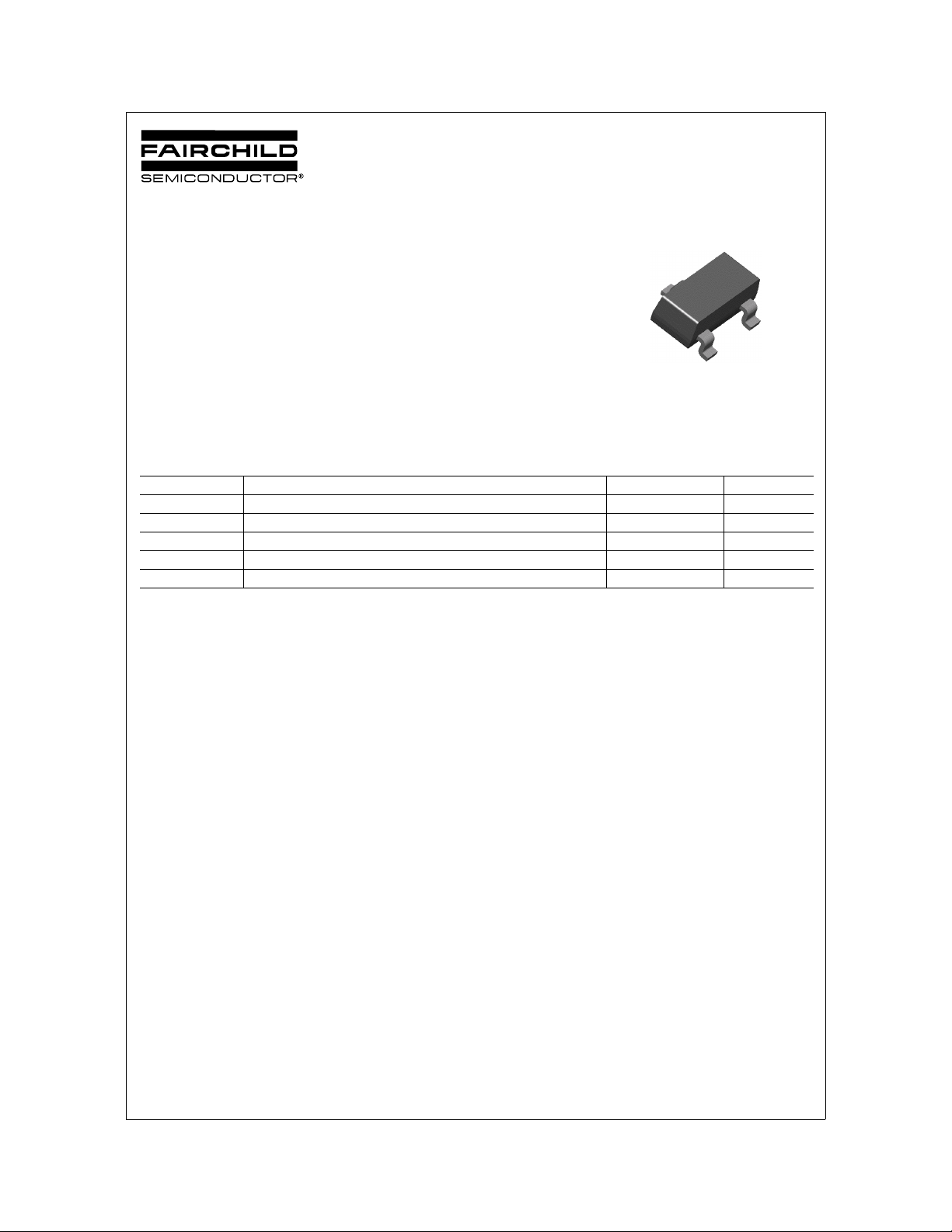
BSR16
PNP General Purpose Amplifier
• This device designed for use as general purpose amplifier and
switches requiring collector currents to 500mA.
• Sourced from Process 63.
• See BCW68G for Characteristics.
PNP Epitaxial Silicon Transistor
3
2
SOT-23
1
Mark: T8
1. Base 2. Emitter 3. Collector
BSR16
Absolute Maximum Ratings*
Symbol Parameter Value Units
V
CEO
V
CBO
V
EBO
I
C
, T
T
J
ST
* These ratings are limiting values above which the serviceability of any semiconductor device may be impaired.
NOTES:
1) These ratings are based on a maximum junction temperature of 150 degrees C.
2) These are steady state limits. The factory should be consulted on applications involving pulsed or low duty cycle operations.
Collector-Emitter Voltage -60 V
Collector-Base Voltage -60 V
Emitter-Base Voltage -5.0 V
Collector Current - Continuous -800 mA
Operating and Storage Junction Temperature Range -55 ~ +150 °C
Ta=25°C unless otherwise noted
©2002 Fairchild Semiconductor Corporation Rev. A, July 2002
BSR16
Electrical Characteristics T
=25°C unless otherwise noted
a
Symbol Parameter Test Condition Min. Typ. Max. Units
Off Characteristics
BV
BV
BV
I
CBO
I
CEX
I
BEX
(BR)CEO
(BR)CBO
(BR)EBO
Collector-Emitter Breakdown Voltage IC = -10mA, IB = 0 -60 V
Collector-Base Breakdown Voltage IC = -100µA, IE = 0 -60 V
Emitter-Base Breakdown Voltage IE = -10µA, IC = 0 -5.0 V
Collector Cut-off Current V
= -50V
CB
= -50V , TA = 150°C
V
CB
-10
-10
Collector Cut-off Current VCE = -30V, VEB = -0.5V -50 nA
Reverse Base Current VCE = -30V, VEB = -3.0V -50 nA
On Characteristics
h
FE
(sat) Collector-Emitter Saturation Voltage IC = -150mA, IB = -15mA
V
CE
(sat) Base-Emitter Saturation Voltage IC = -150mA, IB = -15mA
V
BE
DC Current Gain IC = -0.1mA, V
I
= -1.0mA, V
C
= -10mA, VCE= -10V
I
C
= -150mA, V
I
C
I
= -500mA, V
C
= -500mA, IB = -50mA
I
C
= -500mA, IB = -50mA
I
C
CE
CE
CE
CE
= -10V
= -10V
= -10V
= -10V
75
100
100
10050300
-0.4
-1.6
-1.3
-2.6
Small Signal Characteristics
f
T
Current Gain Bandwidth Product IC = -50mA, V
f = 100MHz, T
C
cb
C
eb
Output Capacitance V
Emitter-Base Capacitance V
= -10V , IE = 0, f = 1.0MHz 8.0 pF
CB
= -2.0V, IE = 0, f = 1.0MHz 30 pF
CB
= -20V,
CE
= 25°C
A
200 MHz
Switching Characteristics
t
on
t
d
t
r
t
off
t
s
t
f
Turn-On Time VCC = -30V, IC = -150mA,
= -15mA
I
Delay Time 10 ns
B1
Rise Time 40 ns
Turn-Off Time VCC = -30V, IC = -150mA,
= IB2 = -15mA
I
Storage Time 80 ns
B1
Fall Time 30 ns
45 ns
100 ns
nA
µA
V
V
V
V
Thermal Characteristics
TA=25°C unless otherwise noted
Symbol Parameter Max. Units
P
D
R
θJA
* Device mounted on FR-4 PCB 40mm × 40mm × 1.5mm
©2002 Fairchild Semiconductor Corporation Rev. A, July 2002
Total Device Dissipation
Derate above 25°C
350
2.8
mW
mW/°C
Thermal Resistance, Junction to Ambient 357 °C/W
 Loading...