BSP50
BSP50
NPN Darlington Transistor
• This device is designed for applications requiring extremly high current
4
gain at collector currents to 500mA.
• Sourced from process 03.
1
3
2
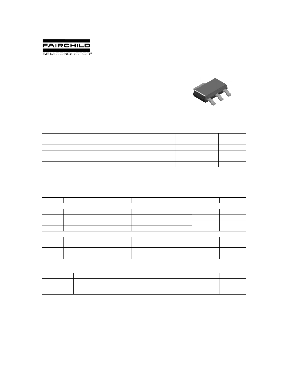
SOT-223
1. Base 2. Collector 3. Emitter
Absolute Maximum Ratings*
Ta=25°C unless otherwise noted
Symbol Parameter Value Units
V
CER
V
CBO
V
EBO
I
C
, T
T
J
STG
* These ratings are limiting values above which the serviceability of any semiconductor device may be impaired.
NOTES:
1) These ratings are based on a maximum junction temperature of 150°C.
2) These are steady state limits. The factory should be consulted on applications involving pulsed or low duty cycle operations.
Electrical Characteristics
Collector-Emitter Voltage 45 V
Collector-Base Voltage 60 V
Emitter-Base Voltage 5 V
Collector Current - Continuous 800 mA
Operating and Storage Junction Temperature Range - 55 ~ +150 °C
Ta=25°C unless otherwise noted
Symbol Parameter Test Conditions Min. Typ. Max. U nits
Off Characteristics
V
(BR)CBO
V
(BR)EBO
I
CES
I
EBO
Collector-Base Breakdown Voltage IC = 100µA, IE = 0 60 V
Emitter-Base Breakdown Voltage IE = 10µA, IC = 0 5 V
Collector Cutoff Current VCE = 45V, VBE = 0 50 nA
Emitter Cutoff Current VEB = 4.0V, IC = 0 50 nA
On Characteristics
h
FE
(sat) Collector-Emitter Saturation Voltage IC = 500mA, IB = 0.5mA 1.3 V
V
CE
(sat) Base-Emitter Saturation Voltage IC = 500mA, IB = 0.5mA 1.9 V
V
BE
DC Current Gain IC = 150mA, VCE = 10V
= 500mA, VCE = 10V
I
C
1000
2000
Thermal Characteristics
TA=25°C unless otherwise noted
Symbol P arameter Max. Units
P
D
R
θJA
©2004 Fairchild Semiconductor Corporation Rev. A, May 2004
To tal Device Dissipation
Derate above 25°C
1000
8.0
mW
mW/°C
Thermal Resistance, Junction to Ambient 125 °C/W

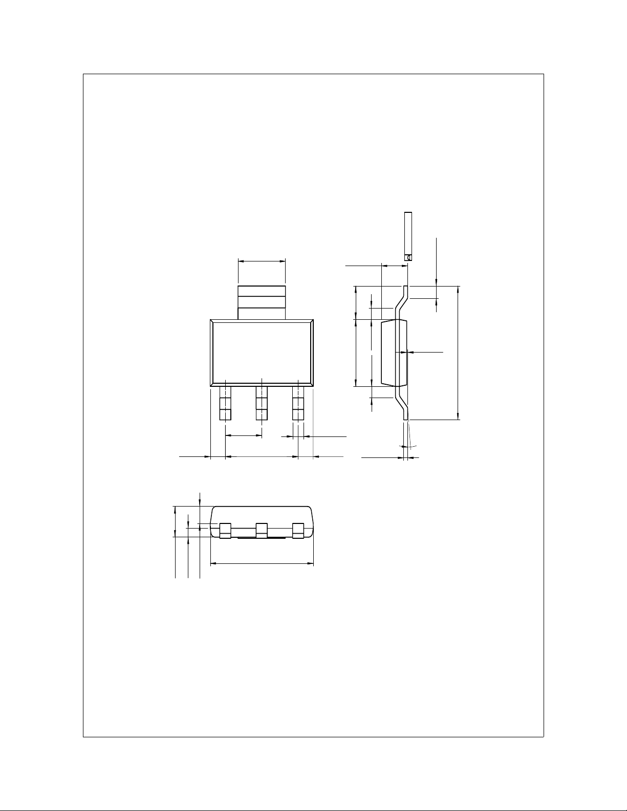
Package Dimensions
SOT-223
3.00
±0.10
MAX1.80
±0.20
1.75
±0.20
0.08MAX
+0.04
0.06
–0.02
BSP50
±0.20
0.65
±0.30
2.30 TYP
(0.95) (0.95)
±0.20
(0.46)
(0.89)
1.60
4.60
6.50
±0.25
±0.20
0.70
±0.10
3.50
(0.60) (0.60)
0.25
+0.10
–0.05
7.00
0°~10°
Dimensions in Millimeters
Rev. A, May 2004©2004 Fairchild Semiconductor Corporation
 Loading...