BF256A/BF256B/BF256C
N-Channel RF Amplifiers
• This device is designed for VHF/UHF amplifiers.
• Sourced from process 50.
BF256A/BF256B/BF256C
350
2.8
6
11
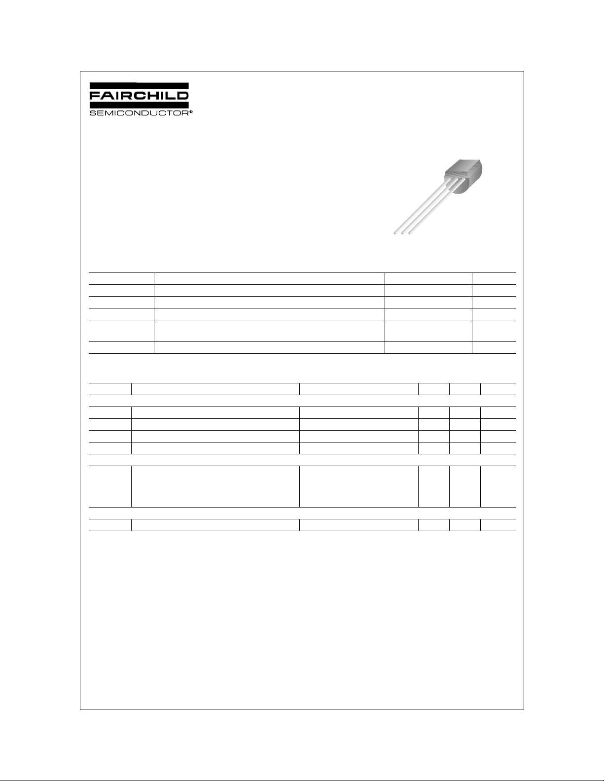
TO-92
mW/°C
7
13
18
1
1. Gate 2. Source 3. Drain
Absolute Maximum Ratings
Symbol Parameter Value Units
V
V
I
P
T
DG
GS
GF
D
STG
Drain-Gate Voltage 30 V
Gate-Source Voltage -30 V
Forward Gate Current 10 mA
Total Device Dissipation @TA=25°C
Derate above 25°C
Operating and storage Temperature Range - 55 ~ 150 °C
Electrical Characteristics
Symbol Parameter Test Condition Min. Max. Units
Off Characteristics
V
(BR)GSS
V
GS
V
GS
I
GSS
On Characteristics
I
DSS
Small Signal Characteristics
gfs Common Source Forward Transconductance V
Gate-Source Breakdown Voltage VDS = 0, IG = 1µA-30V
Gate-Source VDS = 15V, ID = 200µA -0.5 -7.5 V
(off) Gate-Source Cutoff Voltage VDS = 15V, ID = 10nA -0.5 -8 V
Gate Reverse Current VGS = -20V, VGS = 0 -5 nA
Zero-Gate Voltage Drain Current
Ta=25°C unless otherwise noted
Ta=25°C unless otherwise noted
BF256A
BF256B
BF256C
= 15V, VGS = 0 3
V
GS
= 15V, VGS = 0, f = 1KHz 4.5 mmhos
DS
mW
mA
©2003 Fairchild Semiconductor Corporation Rev. A, June 2003

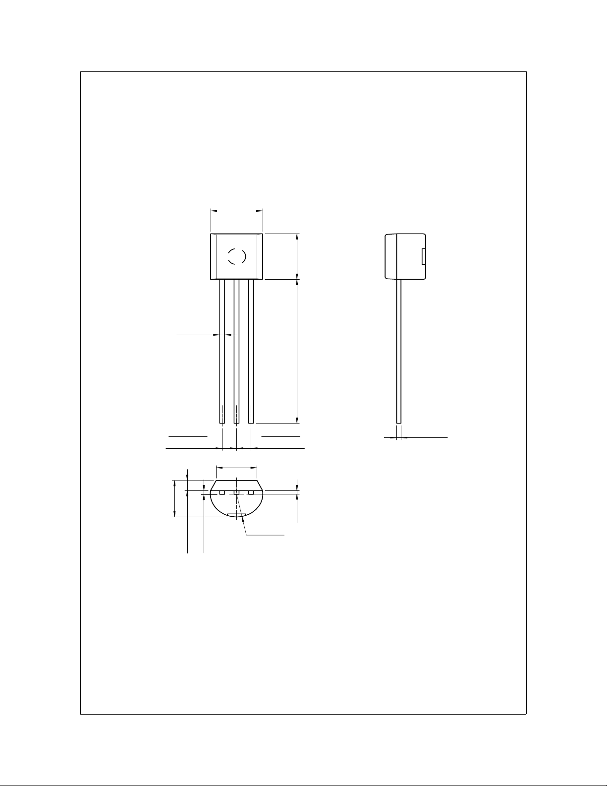
Package Dimensions
0.46
±0.10
4.58
+0.25
–0.15
BF256A/BF256B/BF256C
TO-92
±0.20
4.58
±0.40
1.27TYP
[1.27
±0.20
3.86MAX
±0.10
1.02
+0.10
–0.05
0.38
14.47
1.27TYP
]
3.60
±0.20
[1.27
±0.20
]
0.38
+0.10
–0.05
(0.25)
(R2.29)
Dimensions in Millimeters
©2003 Fairchild Semiconductor Corporation Rev. A, June 2003
 Loading...