

BCW71
C
BCW71
E
SOT-23
Mark: K1
B
NPN General Purpose Amplifier
This device is designed for general purpose amplifier
applications at collector currents to 300 mA. Sourced from
Process 10.
Absolute Maximum Ratings* TA = 25°C unless otherwise noted
Symbol Parameter Value Units
V
CEO
V
CES
V
EBO
I
C
TJ, T
stg
*These ratings are limiting values above which the serviceability of any semiconductor device may be impaired.
NOTES:
1) These ratings are based on a maximum junction temperature of 150 degrees C.
2) These are steady state limits. The factory should be consulted on applications involving pulsed or low duty cycle operations.
Thermal Characteristics TA = 25°C unless otherwise noted
Collector-Emitter V ol tage 45 V
Collector-Base Voltage 50 V
Emitter-Base Volt age 5.0 V
Collector Current - Continuous 500 mA
Operating and Storage Junction Temperature Range -55 to +150
°
C
3
Symbol Characteristic Max Units
*BCW71
P
D
R
JA
θ
Total Device Dissipation
Derate above 25°C
Thermal Resistance, Junction to Ambient 357
350
2.8
*Device mounted on FR-4 PCB 40 mm X 40 mm X 1.5 mm.
1997 Fairchild Semiconductor Corporation
mW
mW/°C
C/W
°
NPN General Purpose Amplifier
(continued)
Electrical Characteristics TA = 25°C unless otherwise noted
Symbol Parameter Test Conditions Min Typ Max Units
OFF CHARACTERISTICS
V
(BR)CEO
V
(BR)CBO
V
(BR)EBO
I
CBO
ON CHARACTERISTICS
h
FE
V
sat
CE(
)
V
sat
BE(
)
V
BE(on)
SMALL SIGNAL CHARACTERISTICS
f
T
C
obo
C
ibo
NF Noise Figure IC = 0.2 mA, VCE = 5.0 V,
Collector-Emitter Break down
IC = 1.0 mA, IB = 0 45 V
Voltage
Collector-Base Breakdown Voltage
Emitter-Base Break down Voltage
= 10 µA, IE = 0
I
C
= 10 µA, IC = 0
I
E
Collector-Cutoff Current VCB = 20 V, IE = 0
= 20 V, IE = 0, TA = 100°C
V
CB
50 V
5.0 V
100
10
DC Current Gain IC = 2.0 mA, VCE = 5.0 V 110 220
Collector-Emitter S aturation Voltage IC = 10 mA, IB = 0.5 mA 0.25 V
Base-Emitter Saturation Voltage IC = 50 mA, IB = 2.5 mA 0.85 V
Base-Emitter On Voltage IC = 2.0 mA, VCE = 5.0 V 0.6 0.75 V
Current Gain - Bandwidth Product IC = 10 mA, VCE = 5.0 V,
330 MHz
f = 35 MHz
Output Capacitance VCE = 10 V, IE = 0, f = 1.0 MHz 4.0 pF
Input Capacitance VEB = 0.5 V, IC = 0, f = 1.0 MHz 9.0 pF
10 dB
= 2.0 kΩ, f = 1.0 kHz,
R
S
BW = 200 Hz
µA
BCW71
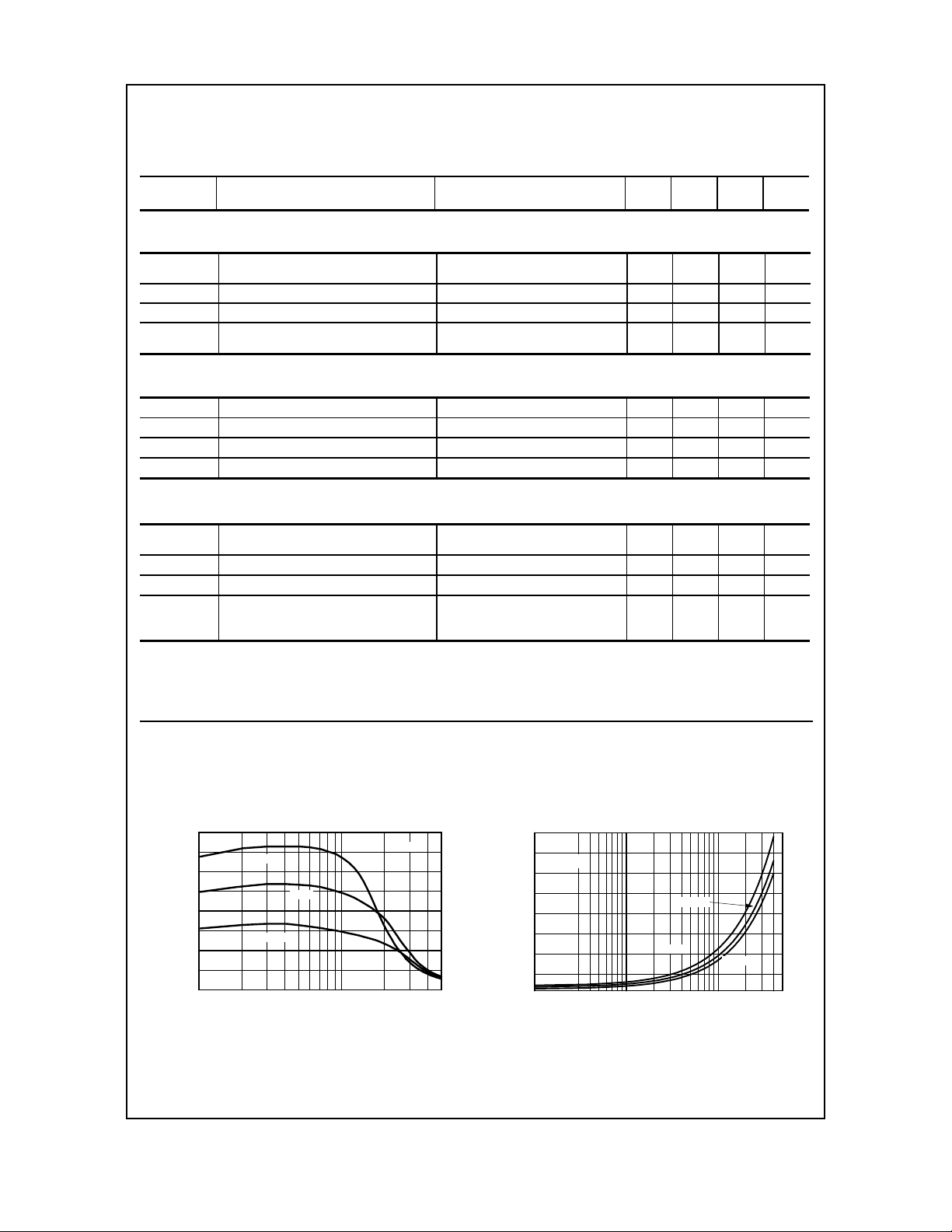
T ypical Characteristics
Typical Pulsed Current Gain
vs Collector Current
400
300
200
100
0
FE
10 20 30 50 100 200 300 500
h - TYPICAL PULSED CURRENT GAIN
125 °C
25 °C
- 40 °C
I - COLLECTOR CURRENT (mA)
C
Vce = 5V
Collector-Emitter Saturation
Voltage vs Collector Current
0.4
= 10
β
0.3
125 °C
25 °C
- 40 °C
0.2
0.1
110100400
CESAT
V - COLLECTOR- EMITTER VOLTAGE (V)
I - COLLECTO R CUR RENT (mA)
C
 Loading...