Fairchild 79-02A Service manual
......r.'r:.
:t:.:.:.:t:.:t:.:;:;:;:.:;:;:;:;:;:;:;:;:;:;:;:::::::::
;!1!;:;l;!;:1!;!::::::::::::::::i:i:i:i:::::::::::i:i:i:
::iii:iai:ai:i::i:i:::i::iii:::rii:iiiii
:iiiiii*i:ii{iiLiiiiiiliiiiii
3:3:3:31;!31;!;!3H::::::Li::::::i::;::':::li:::::f
..r;.;!:.;r-.-.:.:.-rlrirlrlrlrlrlrlrir]-r
I:I:I:l:l:l:l:l.I.l.l.I{,!.1.1.}:.:.:f
i:iilli:i:i:Hii:Iliil::ttlifli:i:
iiililiililil:+iii::::::::
;:g:3:;:;l;!31;l;:;ffi
!::::.:t:!i:i{l:;1.::fi
I:i:ii:::i:fi iitiii:=ii:iiii!
!31131!13131
i::.:::::iaii::i{t:::
:l
ru
79.02A
lnrlrucllon
Sorlol
DUAI.,
No.
TRACE
Mo n
PLUG-IN
uol
#fiffffiiw
fi!####**#ffi
This Plug-In Module
rrith the
Oscl llos cope .
FAIFICHILtrI
lNSTRUMENTATION
.
o'r,r'oa
or,..rcir!o
50
c..a.a
sol,tERsET PIACE,
co.ror.rroi
CLIFTON,
Fairchild
NEV| iIERSiEY,
Type 766H/E Series
designed
is
U.S.A.
for
use
O
lru
toi..hila
C.i....nd
li.rrur.nt
Ccrr.
r
.n!or No.
67
04 55L2
II
IABLE OE'CONTENTS
section
1.
:2.
2-7
2-8
2-9
2-10
2-LL
2-t2
2-L4
1-1
L-2
1-3
2-L
2-2
2-3
2-4
2-5
2-6
TECHNICAL
ST'MIIIARY
fntroduction
Features
Technical
Type
?9-02A
Summary
Nominal
curve
OPERATING
First
Time operation
Applying
DC Balance
Settlng
INSTRUCTIONS
a Signal
Adj
Gain
of Dual-Trace
Input-Selector
obtaining
Cabling
UEe
of
Dual-Trace
Dual
Trace
Setting
a Display
Techniques
Probes
Operation
friggering
Up.Amplifier
Sensitivity
Voltage
!{easuring
Measurement
Short
Title
(Speci
ustnent
Switch
in
s
Rise
fi cations
Freguency
Amplif,ier
the
Nanosecond
for
creater
Eines
)
Response
.
Input
Realm
Page
1-r
1-1
l-2
1-5
2-L
2-L
2-L
2-2
2-4
2-7
2-8
2-L6
2-20
2-2L
2-22
2-22
2-26
3.
4.
5.
4-t
4-2
4-3
4-4
4-5
4-6
5-1
5-2
5-3
5-4
5-5
5-6
FT'NCTIONAL
PERFORMANCE
Maintenance
Checking
Checking
Checking
Checklng
Checking
MAf
NTENANCE
BLOCK
ASSUR.A}ICE
Check
DC Balance
Sensitivity
Fast
r'rode
Chopped
A].tD
Introduction
Removal
servicing
Gaining
Test.Equipment
Adl
Gas
Compensation
Access
us
tments
and
Replacement
Hints
DTAGBAMT;
TEST
to
Assure
Adjustment
oi
Rise
Switch
Tirne
Operation
RECAIJIBRATION
to
Chassis
Required
Adj
ustments
performance
Channels
of
Channels
parts
of
for
Service
1
s 2
1
4-I
4-2
p
4-2
4-3
4-4
4-4
s-1
5-1
5-t
5-4
5-4
5-6
III
section
5.
.
6.
(concluded)
5-7
5-8
5-9
5-10
5-11
5-12
s-13
5-14
5-1s
5-16
TABIJE OF
(contiauea)
DC
and Bridge Bal
Invert Balance
X10 lJevel
Output
Gain Adj
x10
Cal Adjustment
Trigger
Channel
High
Freguency
Input
Attenuator
ELECTRICAL
LTST
OF
Adjustment
Current
ustments
DC Level
2
Output
Capacitance
Adj
PARTS
RECOMMENDED
CONTENTS
Title
Adj
ustrnent
Adj
ustment
AdJ
ustment
AdJ
ustment
lJevel
: AdJ
ustnenta
Standardizatlon
ustment
LIST
Adj
AriID
VENDORS
ustt0ent
arnd
SCHEMATICS
Page
5-6
5-7
5-8
5-9
5-9
5-10
5-10
5-11
5-11
5-17
Number
5-l
Figure
l-1
2-L
2-2.
2-3
2-4
to
2-9
to
2-L2
2-t3
2-8
2-ll
Attenuator
Type
79-02A
Punction
Punction.
Switchlng
Type
79-02A
waveforn
Waveform
Compensation
IIJLUSTRA?IONS
Dual
of
Type
of, Tlpe
Facilities
Calibrator
Displays
DisplayE
Peak-to-Peak
Instantaneous
Respect
to a
TABLE
TitIe
Title
Trace
7g-O2A
79-O2A
Voltage
Voltage
Reference
Trimners
100
Mc Amplifier
Dual
fnput
Channel
Channel
Display
Measurements
Measurement
potential
with
Controls
Page
5-21
Page
1-0
2-3
2-5
2-6
2-9
2-L3
2-18
2-L9
2-24
2-26
to
&
IV
Flgure
3-1
3-2
3-3
3-4
3-5
TABLE OE
type
79-024 Input
Functional
Type
79-02A
Functional
lype
Type 79-02A
79-02A
Block
Diagrarn
Functional
Type
79-02A Y Deflection
Functional
CONTENTS
(Concluded)
IIJLUSTRATIONS
(concluded)
Tirle
Circuit,
Block
Channels
Block
XlO AnplifierE,
Electronic
Block
Block
Diagram
I & 2
Diagran
Suitching
Diagran
Amplifier,
Diagratn
Slmplified
-
pre-Amp1lfiers.
Functlonal
Circuit,
Page
3-2
3-3
3-4
3-5
3-5
3-6
5-l
5-2
5-3
5-4
5-5
5-5
5-7
5-8
5-9
5-10
5-II
6-l
Type
?9-O2A
Functional
rlpe
Iest.
Appearance
Left
Test
79-02A
Setup
Trimners
Side Vler
-Setup
and Volts,/Div
Standardizing
Left
'Right
Left
Left
Side
Channel
Side
Side
Side
View
2
View
View
Adjustments
?op
View Showing
Pot
Adjustments
Front
Panel
Trigger
Block
Over-AlI
Amplifiers,
Di agram
System
For Mjusting
of Wavaf,orm
Showing
when
ttF:
for AdJusting
ErLnrmers
the
Input
Showing
Attenuator
View
Replaceable
Showing
Showing
Showing
Delay
Channel
Adjustments
Transistors
Trimmers
Line
Block
H19h
Making
Diagram
Freguency
High
Trimners
fnput
Capacitance
Capacltance
I and
Nuvistors
Trimmer
6
Transistors
pot
and
and
parts
3-7
5-2
5-L2
5-16
5-lg
5-I9
5_ZO
S-22
5_23
5_24
S-25
6_0
tE
{-o
G'T
f,tu.!
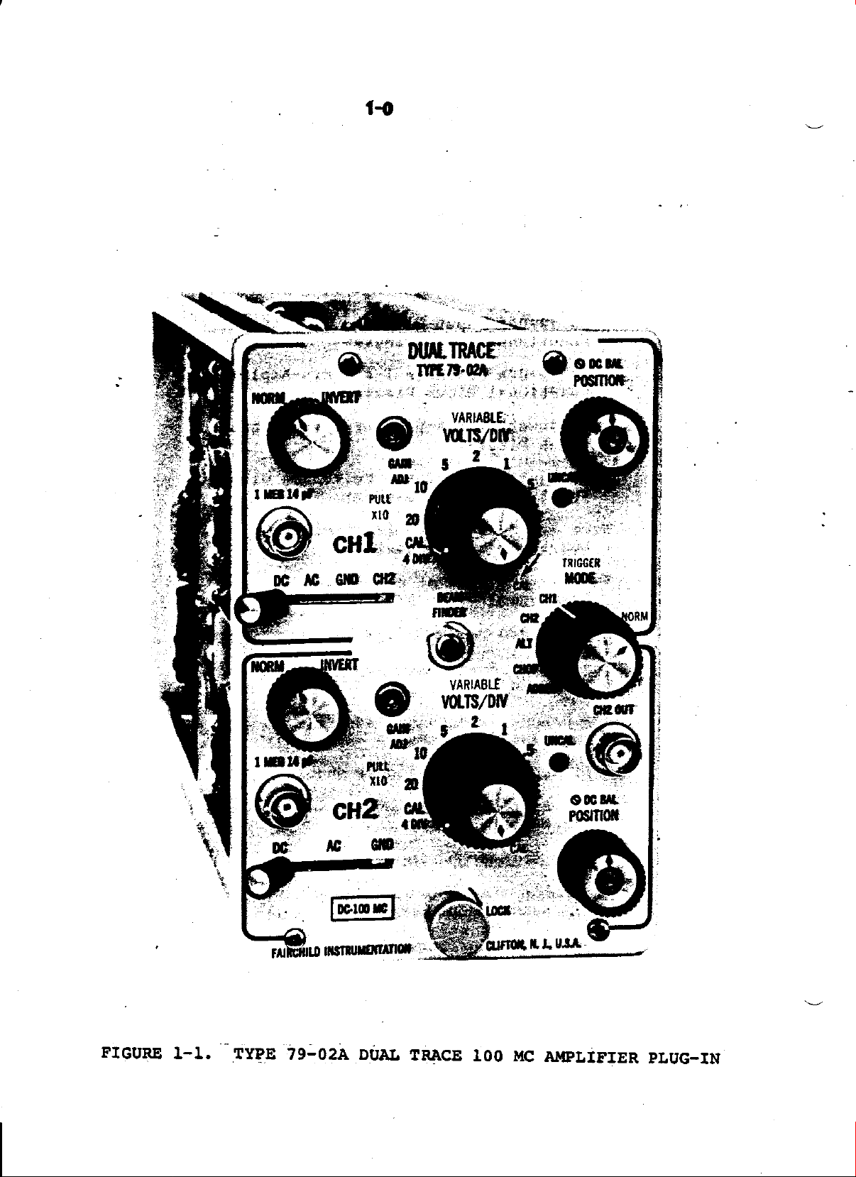
FIGURE
1.I.
lOO UC
AII{PLIPIER
PLUG.IN
1-1
I-1. INTRODUCTION
The
lype 79-02A
provided
for
Xl anit
t
ith
100 millivolts,/divigion
I00 negacycle
10 mtlllvolts,/divlsion
90 negacycle
"
-
operation
vertical-
elther
I_I3_YMlpE.ga1n
voElS,/DIv
This
steps
vAltABr.E galn
of the
posltlon
of this
sigrnals
channel
sritch,
is
SEETION
TECMTICAII
Anpllfter
ie-a
tuo basie an6rl1lier
X10
callbrated operation
banduidth.
banctwidth.
plug-in
on the
unlt
screen
indlvidtually.
control,
has a
contror
attenuatoa
provided
rrnge
(t
when
OLIS,/DIV)
the
1
SUUIIARY
dual-channel
sensltivttiei
as
sensitlvity
sensitivity
enabres
sinultaneousLy
toeated
of
provid;s
concentrically
greater
contr.nuous
sgrltch.
VARTABLE
anplifier
follorrs:
t
ith a dc
wl,th
the
us6!
than
e
gain
contioi
and
bandridthE
to
a
dc
to
to
obtaln
or to
trrsplay
wlrh
2-i,/2
to 1.
ovlrrip
detentid
-is-s"t
and
is
two
the
betrreen
stop
to cAL.
1.2.
A loDE
channer
of
both
csoPp€d
rnversl,on
minus
The type
switch
1
channels-
modes
channel
the Aype
EEATT'RES
.IOO
o10
.Solld
a
Carcading
!I19?.to.a
sensltl,vity
!{c
bandntdth
nv,/dlv
state
provided
is
or channel
for
of
operatr.on
srrl.tch
7g-o2!.
766Id/?
nay
preientatlon
I
Anplifler
Serl,eg
aensitl,vlty
clrcuitry
feature
hlgh-galn,
with
2
for
duar
glve
Oscilloscopes.
at
100 mrldiv
wlth
converts
single
Mc
30
bandvidth
which
Eeparate
dlspray.
are
channel
enabres
dlsplay
rn
avairable.
I rnl.nus
when
lpDE
is-intended
sensltivlty
90
t{c
bandnidth
Lnstrurnent
trace
unlt;
nominal.
the
serection
or the
iaaition,
use
channel
srritch
for uge
fron
dual
1
nv,/div
comuination
elreinate
6f
itre-ioriri[y
-or-
i
ig
set
in
the
of
either
or
crrannei
io aooeo.
y
cavity
z
of
L-2
EEATURES
Front-panel
O
channe I
O Polarity Inversion
(concluded)
to nor:nall za
tro slgnala
Ground
o
groutrd.
grounding
ProvLder
a
-
used
'
Th6 Base
posl,tion
refercnce
wlth
l-3. IECBNICAL
fhe electrl,cal
ar€ llrted
GAIN AD,
when
operating
on Input
on bage
input
of
eguivalent
Falrchild
Plug-ln
SUUUARY
untt'
(Speclfications)
characterlatics
in the
perfor:nance
control is
galn
grl,tch
betrreen
enableg
ln
Sel€ctor
llne
inatrunent
dual-bean
Type
Z{-IZA
.
prorri
ded
channels
for each
subtraction
the
Added
srl,tclr
without
scope
lutonltic
of
thc Tlr;le
rcde
provides
nec-aalty
operation
Display
speclficalion
of
of
when
79-O2A Anplifior
whl.ch
foifowi.-
..
1-3
SPECIFICATIONS
Y N{PI,IFIER
Bandwidth
Direct
XI:
X10: DC
Coupled:
DC to approximately
100 megacycles.
to approximately
90 megacycles.
Capacitively
-or
xl
Rise
Xl:
X10:
NOTE:
xlo:
Time:
3.8 nanoseconds
4.2 nanosecondg
Rise
should
Coupled:
Low-frequency
cutoff
cycles.
tine
be 0.4
of Test
is 16
nsec
or 1ess.
or less.
Generator
or better.
Output
Six
scan
Ranoe
divisions
(D3
and
available.
are
each
Input
I
megohn
Input
Channel
4-position
permits
coupling,
ground.
rrith
providing
coupling
a
position
reference
sigmal.
3t at
Impedance
shunted
Selector
I is
selection
Channel
3-position
and
provides
of
vertical
D4
CRT
Overshoot
4-division
by
Switch
provided
lever
switch
of
Channel
2
2
levei
selection
ground.
base
and
disconnects
plates)
and
14 pf.
lrlth
whL ch
a-c
output
provided
is
switch
of
a-c
The
line
output
ii
preswins
ican.
a
or
d-c
or
or
d-c
cND
input
SenEitivity
Cal XI:
Cal
XIO:
Uncal,
XI
or
X10:
100
millivolts,/div.
to 20 volts,/divlsion
in
8 steps
5 sequence
gain
CAL;
+3t
Etep.
10 ni1llvolts,/divislon
to 2
13 and
control
6ssusste
when
voLts/division
Continuouslyvariable
fron
to
VARIABLE gain
10 mil11volts,/dlv.
50 volts,/div.
permits
continuous
adJ
ustments
attenuator
extends
range
to
of 1,
lrhen VARIABLE
is set
to lrithln
set on
5
sequence.
control
2-L/2
to
sensitivity
between
steps
the
20 volts,/div.
50
volts,/div.
2,
any one
fhe
L
and
and
to
in
the
Polarlty
Separate
seritch
selection
fNVERTed
Inversion
two-position
for
each
of
either
input
Callbration
Calibrator
square
to
to--standardize
DIV
(Cal.:
in
wave)
the
input
slritch
/t
the
XI position.
signal
is
of
is
divisions
_
channel
signal.
applied
the
gain
set
to
;
rotary
NORMaI
(line
y
Ampllfier
rdhen
CAL.
valid
)
proiides
or
frequencv
airedtly
VOLTS/
only
'
1_4
SPECIFICATIONS
Signal Delay
A
l8S-nanosecond balanced
-
distributed bl.fllar helical
delay
delay
basellne
line is
ls
sufficient to vier
and th€
of a fast
for intornal
the
titn6 base.
Interrral
A
tso-position suitch providea
a trigger
stage
trlgger
2 only.
Triaqer
plck-off
(Ch
I and Ch
pick-off
provided.
leadlng
rise-tirne
trlggerlng
from
signal
after
2)
or a
Channel
This
edge
of
Ewltch
(Concluded)
Y AIDI..IFIER
Operational
The
avaLlable:
follorlng
1.
Ch
2.
Ch
I
2
3. Ch 1
Modes
displays
only
only
e Ch 2.swltched
alternately
4.
Ch 1
(chopped)
5. Ch
s
Ch 2 tima
I
S Ch 2
(Invert
permitsChl-Ch2or
Ch2-Chlpresentation)
are
shared
swltch
-
The
interrral trigger
sigmal
when
to
Is
the trace
acreen
adjustnent
control.
An
lnternal
Channel
Channel
provlde
the
Channel
2
I lnput
a serles
anpllflers.
noted
channela
operation
featur€
Avallable
div
Mc
noroinal.
that only
ar6
us€ful.
and ban&rldth
in
thls mode.
referenced
positioned
ls
center vla
of
the Trig
connection
output
1
lc
connector
connector
connectlon
and
Channel 2
It
should
when
sot
up
the
cascadlng
for
sensitivlty
is
30
output
ground
to
factory
DC
LEVEL
from
can
be
th€
XIO
ie
I
dc
to 25
Mc
to
of
nv,/
6.
Cascaded
In
chopped
chopping
are
available
internal
translents
bltnked.
Bgam
A
slritch
locatlon
posltloned
Flnder
-
sprlng-Joaded puah-button
is
of beam
operation.
operation,
rates,
100
and
Fwitch.
are
autonatically
provided
off
screen.
fc
selected
Switchlng
to
when
two
and 1
!{c,
by an
facllitate
lt
is
a
!
a
A/
IA
I
I
I
It
2
6
a-5
o
o
G,
.
lrl
G
3
o
lrl
o
2
o
L
U'
trJ
G
l
I
I
e
o
JO
(J
trl
a
lll
3,tr
J
irz
;=
z
;z
al
o
I
o
N
L,
o.
o
F
ONT(,OOGlr'@(D
',rtTT;TT
s138rC30
r{l
Ntvo
ONrtlo
NGrGl6l
tlll
2-l
2-1.
.
OPERATING
FIRST
The
Y cavity
Base
i" !lr:
oscirloscopes.
Type
rn
indj.cate
Note:
The.
in
The
to extend
TIME
Type 7?-02A
OPERATTON
Duar ?racq
(left-hand
Plug-in
cavity
X
7062 CRT
(other
(right-hand
The
Termination
the instructions-vrhich
front-panel
pf9p9r
I'or
installed_only
Frane
following
becorning
Figure
Fisure
Figure
remaining
Oscilloscope.
ilrustrations
familiar
2-1,.
2-2.
2-3.
the
Function
Iungllol
Faci
e,pe
paragraplrs
operatorr
sEcTroN
INSTRUCTIONS
(Figures
Amplrfier
side)
and
Fairchild
side)
E,/r series
Net\rork
forlow,
controls,
performance,
the
y
in
'are
with
the oscill5scope:
of Type
of rype
litieE
?9-02A
s skill
Calibrator
of
this
2
2-t
to
2-3)
plug-in
aEsume
plug-ins
X
oscilroscopls
thaf
may
oi
the
H,zi
to
accoirmodate
capital
conneitorE
make
cavity
desigmed
certain
of
7}-OZA
7g-O2A
the
to
Dual
rnput
Dlsplay
section
in
using
are
the
is inserted
tne rype
be-ised)
Series-ilain
is
retters
or
settings.'
the Type
x,/r
aid the
Channel
ChannEr-iri-"ti"g
provided
iirstrunent.
ia_oie-r-iil-
providect
the Type
withiir
79_02A
Siiles
operator
controls
as
in
is
inseitea
rrame
with
th;
uain
a
the
the
7g-02A.
i&i
is
:
guide
2.2.
2-3.
APPLYTNG
The
signal
(or-both)
performance,
cable,
oscillosco.ra
?he
Fairchild
available
DC
BALANCE
If
the DC
adjusted,
when
BArJ
the VARTABLE
front-paner
1. set
2.
set
A
input
with
for
ADi'USTMEN?
balance
the reference
the IipDE
the voLTs/Drv
control
3. Adjust
obtain
the Time
a
SIGNAL
(or
signals)
connector
the
siglgr
the
shield
and
the
Types
use with
of
control
screwdri.ver
svritch
to
its
reference
to
be displayed
on
the
shourd
connected
signal
.79948
source.j
and
79998
the Aype
the. Type
traEe
Z9-O2A
dn
iE
rotated.
contror
to
cH
I
switch
minlmum gain
Base
plug-in
trace
to
on
-froit.
be
appliid
to
lire
AcceEsory
?9-O2A
Amplifier
the
scieen
for
and
the
posi.tion
o.l
setting.
contrors
the
screen.
is applied
panel'.'
through
chassis-of
probes
to
either
io
rnsuie proper
i
strieraea
both
are
Anpli?iei:
is not
wi1l
propeilv-aaiist
ro
be
properly
depositioned
chilnei-i; pi6.."a
rnput
selector
and
for
automatic
swi.tch
rotate
the
the
aE
the
VARTABLE
sweep
Dc
forlows:
to
cND.
to
4.
5.
5.
Adjust
the
trace
Rotate
its.
range
vertical
-
Adjust
bring
the
the
PoSITION
at center
the
VARIABLE
observing
ly.
the
f,ront-panel
trace
back
2-2
control
on.each plug-in,
of screen
control
the
dlrection
DC BAL
to
center
right
(referinc6
and
left
that
the trace-shiits
screwdriver
of screen.
to
line).
throughout
control
place
'
to
2-4.
Note:
7.
-C-91!1lyg
VARTABLE
placenent
rotated
8.
Repeat- preceding
controlE
Note:
SEATING
whenever
Frane
cArN
to
!9
Plug-in
and
ADJ
conpensate
nroeerly
Do
throughout
.
II !lr9
DC
Sectlon
for
j
ad
GAIN
-the
unit
OF
Type
inserted
contror
normalize
and
not
change
adjustlng
control
of
back
the
trace when
steps
adrustment
BAL
control
5,
the
contrrletE
ulrtment
DUAL-TRACE
79'o2A
in
must
for
the lr{ain
be
difference
the
the POSITfON
the DC
its
is
Irtaintenance
prosedure.
BAL
and
forth,
the-VARIABLE
range.
for
Channel
range
insufficient,
Coarse
A.I,IPIJIFIER
Arnplifie.is
another,
the.front-panel
reset.
in
deflecilon
gain
Frame,
betdiren
control
controt
untll
2
of
the
and
Recalibration,
and
Fine
removed
This
pioceea
proiedur"
channels
settings.
white
there
rotating
is ninimurn-dis-
con.trol
is
using pertinent
front-panel
refer
Balance
to
from
the
screwdrivei
-"J""s"irv
i"
prate
"errsiiiviti.".
or
between
as
follolrs
s
the
uain
the
l. Set
2.
3.
l.
5.
se
5. Adjust
for
both
CAL and
Push
Set
in
IPDE
Mjust
trigge
Set
ring.
II{oDE
conds/divi
4
divisions
the
channer
7. PoEition
8. Adjust
be
Channel
observed
Channel
turn
both
both
VARIABLE
switch
Sweep
switch
s
ion.
the
traces
(traces
I and
VARTABLE
to
CE
controls
to
ALT
I
cArN
of
vertical
one
2
GAIN ADJ
are
Channe
I
2 VOLTS,/DIV
controls
controls
I and
for
and
adjust
AD.r
front-panel
(Xl
TRIG@R
auto
aefflciion.
on
top
of
control
superinpoEed).
to
CAf.
position).
slritch
sweep
aweep
the
until
rate
screwdriver
other.
only
slritches
tfuf:.i-cwi.
to NORIU.
and
line
for 2 rnitli_
one trace
to
contror
may
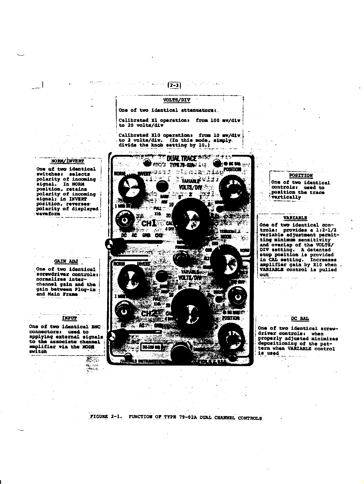
_-l
l?li
voLag/prv
otra o! tro ldaltlcrl rttaDnacolr r
crllbrrt d rl olrr.tlotr
toltt/dlr
to 20
C.ll,bnt.d
volt
tso 2
dlvld. th.
U0
/dlr.
!.!ob
ql.8rttor
(la
thl,r
.!!tlu? uy
lsr. l0 rrldly
Dd., rlq)lt.
lo-.1_ _
-
l
l-
I
I
:
__
-
DOt
tttor
otla
ot
tto
e!t8ol.t
itprltlotr
v.rtlcru,i
f
vritAa&t
O[a ot
trol. r
vrsl.bl. .drq.tDrg
th,
ura
DIV rattlnE. t' d.t atad
.top
l!
eDUll.r
Yr.RIrEtl eoltrol
0ut
tro
Drovld.r
.t!l,
2-1
2-5.
.
'
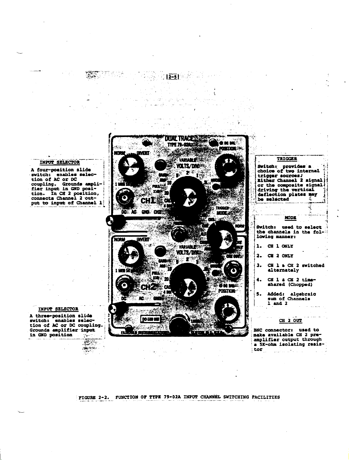
INPIXT
Each channel
which
a
a
Channel 1 Input Selector switch
posltlon
from
nected
technique
function
bandrridth and a sensitivity'of
lhe
level
input
If
signal,.
a! any instant
with
SEI.ESTOR
SWITCH
is
provides
AC
Ground
DC
or
reference
labeled CH 2. In
the output
the following
coupling of input
in series with
converts
to
a
high
Input Selector
the
of
input signal or
signal by
it is desired
set this
ls a function
respect to
provided
with
an
cotnmon
signal
posj.tions
this
of Channel
the
plug-in
the
gain
switch
2 amplifier
input
single
pernits
blocking
inserting a capacitor
to.display both
switch
to
DC.
of
ground.
Input
is
positlon,
Selector slditch
functions s
provided
with
an internal
an additional
is automatically
of Channel 1 arnplifier.
from
trace
I
Thus, the
its normal 100
am5llifier with
Mc
a
nillivolt,/illvision.
cholce
the dc component
in series
the ac and dc corqronents
the instantaneous
retaining
of
rrith
position-
of the display
signal voltige-
connection
con-
This
dual
50 Mc
the
trace
DC
of the
the
input.
of a
There
display.
placed
component while
be displayed.
snitch
excluded frorn
It
to
Amplifier
distortion
display
offs.
resPonse
When
desire
9f
lave
is set
other.i^rords,
negative-going
are times when
dc component
the
in
serieE
j.s
set
to AC. The
the dLsplay.
should
the
be noted
position,
AC
is about
and loss
contains
UEe of a
to 1.6
using.the
to
invert the
the- Polarity
the
same
polarity
to IlitvER?,
a
It is neither
of
the
rrith
simultaneously permitting
This
the input
is
accomplished
effect
that when the
the
lorrest
16 cycles. theiefor-,,
of amplitude
frequency
10:1 Attenuator
cycles.
dual-trace
displayed
fnversion
the
displayed
positive-going
puIse.
components
features
slritch,
as
the
waveform.
applied
pulse
necessary nor
input
connector
!,raveform.
when
of the
.
hput Selector
freguency
wlll
probe
occur
below
brings
of the Type
the displayed
sigiral.
waveform
will
desirable
A
capacltor
wil1
the
exclude
ac
component
the
the fnput Selector
dc
component is now
limit
some
if the
switch
(3
db)
low-freguency
is set
of
pattern
the speiified
the
1ow freguency
I;-
the NoRM
will
be
be
displayed
Z9-O2Ar
wavefolm
When
inverted.
lou
p6sition
re
as a
to
dc
to
the
on
cut-
mat
will
switch
In
-a:\!,
.'
..
i
!i;l
.
INBI'I SB,ECIION
A forr!-porltlo! rlld.
sirltchr .Drblar ralac-
tlo. ol
couplhE. Groqldr
llEr lnput la
tLon. lE CB 2
con!.qEr
puc
1fia..-Po.1gio! alld.
.A
lettei:
tlon ol lC
G!out!& .Epufl.r-lEtrrt
lE c D
lC
Dc
or
po.l-
OID
poaltloB,
Ch.n!.l, 2 oEt-
to LnPEts ol c!.n!.l I
sBt.lqlot
tt{P08
.ubr.a. ..1.e
ga
DC coupulg.
po.ltloa
.1a1" .
&pll-
_i:,,.r
titcGBn
CT 1 o.ILI
t.
CA Z OILI I
a.
t.
ClltCE2.eitch.d.
a1!ara.taly
CEl,&CB2tlr-
.h.a.d
5-
lad.al! rlg.bral,q
!u! ot Chanr.la
1tld2
(ClppF.dl
@,
.
BIC c@lactort
a.l. avalhbL
olrlr^ll.r
5tr-ob lrol.tl,ng a..1,.-
r
tgr
utad to
p!.-
ca 2
ontput throtrgb
'
Itql
f,..dru.t
and
sA.rD prtt
(9
S.t Poatllog
to caDtar
Aatlc
to
c.a!.E
llfEf,arrt,
colrtror,r tor r
of !a!ga
S.t
S.t
out
(VOmg,/D:Vr--to
,
sr. t
tb. dl,rpt.tl
clattrol,!
t0 rf(,Ea
to Dc
's.t.
r kEob
'OCUS
.llqat
CrL
obtrh tba
ilo
!!I.ctly
iaaqqaoca.
ula th.
,.!
obt.LDlDg
tEoublaa
c.ll,bntor
..
!hor!
.!a
ll.r!o!!
r.!.
ilrocadu!.
(U.pl.r.
.
dua to Elaallgrr{nt
viaE
dt.plat,
tI. ruDb.r.at
allllculty
!rt. rltt
ol
rat
tha coutrol.
cf-Ufaeij
codtsoi,a.
pr
tt
tr
cpctracra l
;co&iit.
18
S.t IAIIG,
ItllEUSItl
'cartaS
&tat.
ttrSD
acoPa
S.t oct
(Il!G/Dlv)
.SlC
t
Botata lnnar knob
(Vfrffr.El
to ClIr
l. acgu.t
i. b.Idr
grc,l&
rOColt
cqttloL
o!
raDg!
cloctrrt.a
o tla
ircb
;
to
cLockyr...
c.otll rrlt.b
d
. Uot
Iap
l. of!
ud
to
,l
Lo
otcillo-
(cUch
tb.t
.
Pulb
lnn.r
lully
lD
aad
(VfRUSL!]
ttroD
clockrl..
sotata
lbritnrr
(?ll@!1,
;
tnol
to lroRn
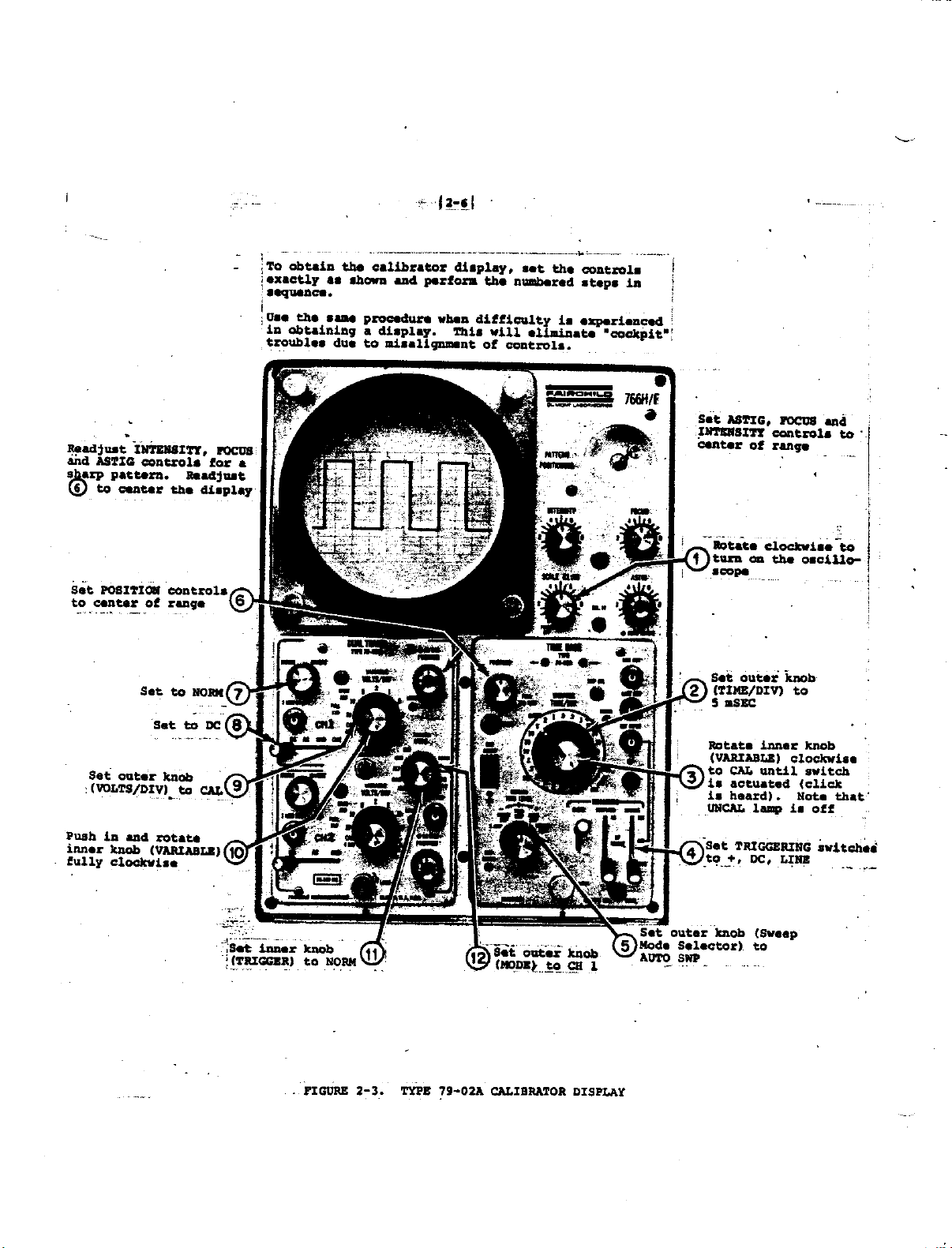
PIGURB 2.3. lYPA
,9.02A
CrI,IBRITOR DISP].AY
Sat
Uod.
n tRtC@RIfG
+,
osta! knob
Salcctos,
DC,
(Sy.cp
to
I.Irl
lyt tch.i
.ii]&..;?,
'.v:.
:.i
1
.:
--inPor'
A tous'-tptltlo.
srlg€b: cD.bl.r
tlon o! lC or DC
cocpllaE. Gronnalt
flor inpqG l! elD
tloE. h CA
cornacta chaEDaL 2
put
sirir'ciloh---
to lnpiiE
tlld.
talac-
8*I-
ito.l- i
po.l,tloD,
2
oqt-
og Cb.!a.L ll
rxPul SEtlc[oB
A tir..-fEtltloE rllda
agitch! anablaa aalas-
tloD ot lC oa
ctoulrdt opull.!
ln(
po.ltloa
D
DC coupllDg.
'lntnE
.i;.
-'
-
l
;
i
.
<air.
cbolca
trlggar aourc.r,
lltt s Ct.l.rl
gr
dalellql
iLll.ctio!
D.
iDNC
jDaI.
opllll.r
a
IBIGGGB.
psovld.r
tre Latarart
ot
2.lgBd
tba eqpalt
tb. v.rtic.l
pht
ralact.d
c@!.ctort
.val,l,.bL
sK-ob lrolatlaq
cs 2
output
uaaA
a
DY
l
n
to
Pr.-
thEough
rqalt-
:PrcuiE
2-2.
Ft NClIOn
Ot It?E 79.02A
T!]PIN
CEATIIIEL SIII'CEING PACILITIES
tgllc
to
o.nr.s
irrEusr*r,
!f.dru.r
rril
sr!!rst, patt
(9
coltrola
ra.
f..drE
th.
troclg
tot .
g
Ct.9l.t
-_
i
obtrla
,fo
,.r.ctlf
rtaq[alca.
I
,
-gt.
lD obt.lnhg
troublaa
r
t'ia crlLbs.tot
a.
tha...r ploc.ar.8.
dua
r'lr:11
tbor! .!d
. dlapl.t.
to dt.llqDErt
Fslotr
alltpl.?,
vh.! dlfllsulty
Ihlr
..!
tna auqb.rad
rLll
.llltart
of cc!t!oI..
tha
coattol.t
.tapa
l.
atp.sl.lcad
t!
-.coer.Lr.
I
:
s.t
tl+ll'lgttt
cantal
t8!IG,
of rargr
noCoS
qttrol.
rai
to
.
S.t POSllld
t"
-i!lt
I
*"
S.t
ont
(VO!45,/DtVl-.to
:
Purh
h .!d
lnn.r
hob
lulli'
clock
coltaolt
ol r.Dg.
r:t
S.t
to DC
r
klob
rgtrta
(tnntABIJl
!,..
Cr&
oElaa
(l.o,D!l
ro_
trrob
-gr
tbtrt
tru!
acoPa
Set oqtoi i<rl
{tlriE,/Drv)
3 ISEC
Rotata lnnar
(VARITEIA,
to CAL untll
la .ctuat
Ir b..rd,
t UCl&
Sat
out.r lnob
liod.
Salacto!)
1
AT'?O SIID
r aR
-_+r
cloch.lr.
tb.
q.clllo-
ro
6
clocl l..
(c!.1c1
d
. Uot. that'
l.e Lr
c@nrnc
E. r4!tt
(Su..t,
to
!o
trob
.rltcb
of!
idt.h;a
-
PICORE 2-3.
TYPE
?9.02T
CAI.IBRAIOR DISPLAT
2-7
2-6.
OBTAINING A DISPLAY
TO
use the Type
as
follows
t.
Signals
:
to be observed are
Amplifier
conEector via shielded cable
2.
Establish a conmon
chassis
To
3.
display a single trace with
simply
set
4.
To display
to each
and the signal source.
apply the signal to
MODE switch
the
Input
or CHOP. The
to
reduce the
input
signal data
div). External
triggering
the srreep
general
and Ehe ALT
the CHOP
,
79-02A Amplifier
through the Channel
ground
to the
two signals simultaneously,
connector
chopped
"flickering"
at slow sweep
triggering
is to be
from triggering
preferred
position
position
with
connected
or
betlteen
either
corresponding
and
set the MODE
position
of
of
on the
is used with
higher
to
obtain
1
andlor
an Attenuator
the
a display, proceed
the
Type
probe.
Z9-O2A
to
Channel- 2 aNC
oscilloscope
the Type 79-02A Amplifier,
Input connector
connect
is used when
the display
speeds
Time
the
(below
Base
in chopped
"chopping"
lower sr,reep
sweep
rates.
channel.
svritch
it
when
or CH
position
signal.
and
a signal
to ALT
is
desired
observing
1 millise-ond,/
2 ONLY
prevent
to
In
rates
Two chopping
selected
transients
To
5.
display
signal
ADDED
To display
6.
signal
ADDED.
Polarity
Inversion
tion,
Channel
8.
Adjust
obtain
o
Set
the
set Channel
the VOLTS,/DIV
desired
rates,
by
an internal slide
100
Kc
are automatically
the algebraic
to each Input
(Ch
+
Ch 2).
the algebraic
to each Input
For
Ch I minus
Inversion
svritch to INVERT.
2 Polarity
switch
Polarity
I
Inversion
sum
connector
difference
conneetor
Ch
the appropriate Time
a stable display
switch
size display
of
and POSITION
positioned
,and
switch.
blanked.
1 Mc,
are available,
Switching
of t'lo signals,
and set
the MODE s$ritch
of two signals,
and set
2 presentati6n,
NORM
to
For
and Channel
Ch 2 minus
fnversion
siritch to NoRM.
Base
the
Plug-in
pattern.
the MODE
switch
control
on screen.
connect
s$ritch
set
Channel
2,
Ch
I
to
controLs
to obtain
a
to
apply a
to
I
polarity
presenta-
ItrtVERT,
to
2-8
2-7.
NOTE:
whenever
the
Main
frequency-
ot
Amplifier.
To make
I.
fulI
!!9
adjustments
Connect
eguipnent
page
the
Frame
5-12
2. Follow
5-I5 a,b,
5-15
CABLTNG TECHNIOI'ES
a.
INTRODUCTIOIT
The pu4)ose
problems
couple
scope
inclusive.
which-may
a signal
over
Type
Sdjustments
possible
7g-O2A Amplifier
and inserted
must
bandwidth
proce€d
r
the Type 79-02A
system
of
described
the Instruction
the instructlons
and
IN
THE NANOSECOND
of
this brief
from
c as
be
described
.
encountered
a
source
a transmisgion
is removed
in anchor,
be
taken
of
the Type
aE follows:
Amplifier
in
Eiqure
Manlal.
outlined
on
RE.A&M
discusslon
when
to
d l0O-megacycle'os6illo-
line.
certain
to
t.r,. iari"iig"
?9_O2A
into
in
pagei
is
one
the
5-2 on
paragraph
i-ii-Iirroustr
point
to
-is
from
trifir_
test
out
trying
the
to
ff
_signal
and
use of
for
microsecond
-fidelity
pasEive
to be inadequate
since
ing device,
to
the
two most
high-frequency
cable
The
to
would
oscilloscope
operator
conserved
rn
to
endr
receiving
the
oscirroscope
be
observed
load
transmission
prevent
the
-which
and
being
comron
and
(2)
rlnging,
cause
discussion
pulse
is
not
by
power
the end
or load
it
the
system
obtaining
is
is
to be
Attenuator
rise-time
for
appli,cation
is
necessarf
some
the
distance
vertical
types
real-time
high
rine
must
measuring
generalry
is
of
transmisslon
oscilloscopes
impedance
reflectl6ns,
deterioration.
properry
is
onry
guaranteed
the
to folrow,
appried
rrhich
at
end.
is
power
maintained,
probes
instruments,
in
tne
used
to
trairsmii
from
input
the
of
paisive
be
designed
and
ay
conirected
optimum
proper
the
carred
wave
end
the
is
received
cabling
which
werE
nanosecond
i= i-i.r*t"
tfr"
source
the
lines
are
and
standing
"ig";f
oscirroscope.
ernploye&
(l)'th;
probe.
connected
insurini
to-the
results,
form
of
the
the
transmission
receivinl
i"-.irr.a-ti"
techniques
satisii-iory
may, prove
realm.
that
t6 tne
waves
that
iirst
ioia...
coaxial
which
trre
source,
but
time
time.
generator
or
rpnitor-
is
The
in
so
as
the
is
rine
:
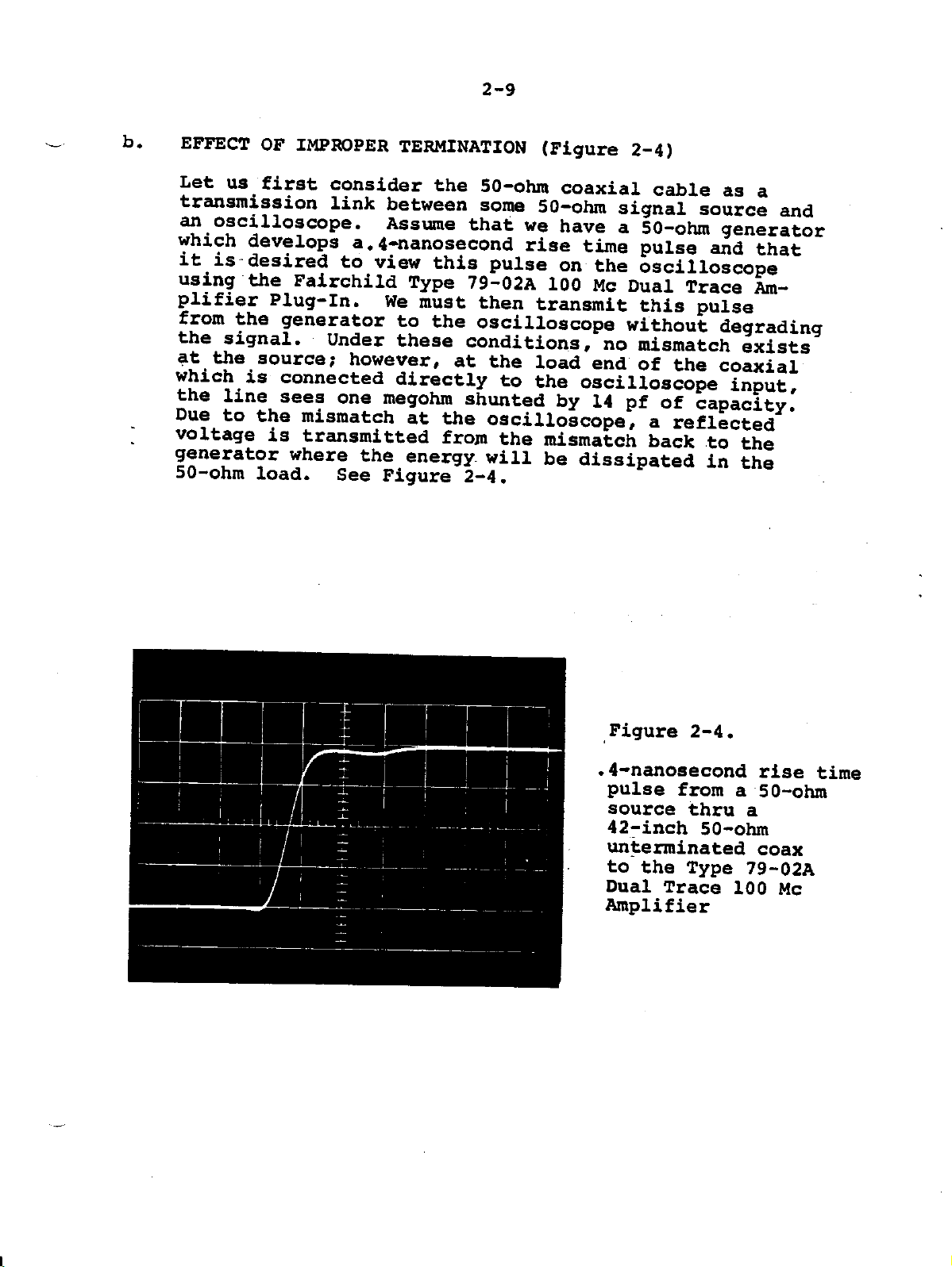
2-9
b.
EAEECT
Let
transmission
OF IMPROPER
us
first
consider
link
an.oscilloscope.
which
it
using
plifier
from
the
e!.the
which
the
Due
voltage
generator
50-ohm
develops
is'deEired
the Falrchild
PIug-In.
generator
the
signal.
sourcei
is connected
line
to
sees
the mismatch
is
transnitted
where
load.
a.
to
Under
hordever,
one megghrn.
See
TERIUTNATION (Aigure
the
50-ohrn
between
Assume
{-nanosecond
view
rype
We
must
to
the
these
directty
at
the
energy.
Figure-
son6
that
rre
rise
this-pulse
79:O2A
then
oscilloscope
transmlt
conditions,'"o
at
the
load'end
to
thJ
shunted
the
oscillo-scope,
from
ttre
will
2-4.
2-4)
coaxial
s0-ohn
have
time putse
o"
it"
lOO
!4c oual
cable
signaf
a
So-otrm
i,scfffoJcope--
Trace
this putse
wittrout
,isrii.h-;;i;;;'
of
the
o"cirfo"cJp"-iil;i;
Uy
fl-ff
rnismilctr
be
dissipated
.i-;;p;i;;:
a
refficiea.
Uacf
as
a
sourc;
t;;.;-t;,
.ria
tfrii--
irn-
_.-
deqradino
"oiiiii-
to-if,.
fn
[tre
and
-
,Figure
.4-nanosecond
pulse
source
42-inch
unlermj.nated
to
the Type
Dual
2-4.
from
thru a
50-ohm
Trace
a
100
Amplifier
rise
s0-ohn
coax
79-02A
Mc
time
2-10
EFFECT
Let
on improper
the-system,
OF
SOURCE AND LOA.D
us examine
terrnination.
there will
more closely the
reflected voltage
voltage and
dlesignated
much
is
If the
as vlewed will be
and
load inpedance approaches
conversely
a short circuit
zero.
a mismatch
occur
optimum
When
causing
terninate
irnpedance.
the coefficient of
as the
greater
than the
if the load impedance
exists and
the transmission
which is
signal deterioration.
response and
the load
See
Figure 2-5. The
at both ends .
IERUINATION
effects
is a
when
a
be
product
a
mismatch
reflected
of
reflection
paranreter
(€).
cable imped.rnce,
infinity,
tlrice the output
the signal
line
not a
pulse
end of thi
perfect
fidelity,
llne
line
(Figure
2-5)
of miEmatch
occurs within
voltage.
the input-signal
which
If
the
load lmpedance
thene
then
of the
generator,
is equal
output
at
the load end
open
circults,
In
order
it is
in its
necesEary
characteristic
is now
This
can be
the signal
to zero,
will
reflections
to.
terminated
-1.
be
sees
obtain
to
It
can be
Pigure
seen
2-4 has
that
been
the
reflection
removed
and
the
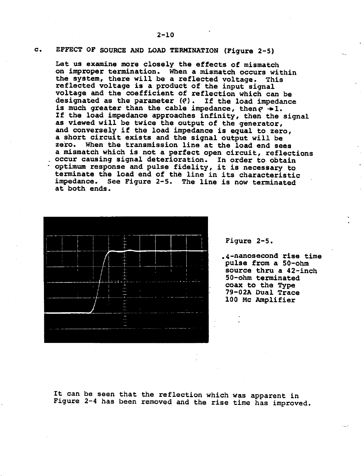
Figure
. 4,-oanosecond
pulse
source
50-ohm
coax
79-02A
100 Mc Amplifier
which
rise
was
time
2-5.
rlse
from a
sO-ofun
thru a 42-inch
teminated
to the lYpe
DuaI
apparent
has
Trace
in
improved.
tinre
By
terrdnating
the reflection
minimized
haE been
and at the
improved.
the
load end of,
due
to
s arne tlme
2-lt
mismatch
the
transmission
at
the
load
the
bandwidth
line,
end has
of the
been
system
at.
EEPECT.OF
whenever
CABLE LENGTE
the- le1Stlr
the bandwidth
cable
the sending
capacity which
and
are terminated
generator
required
:19lif
th?
ls
See
Figure
sees a
to drive
anplitude
improvement
2-6.
of,
of
the system
receiving
in the
resistive
the
iE
not
to
ON PTLSE
RESPONSE
the unterminated
is
reduced
generator
the
ends
of
the
characteristic
load,
and
llne capacity.
paranount
systeh
response
Lf the
(Figures
cable
due
to the
muEt
drlve. Vthen
transmission
impedance,
therefore
The
reduction
primary
2-6
is increased,
increased
the
is
no
otii-tive
and-pulse'fia6fiiy.-
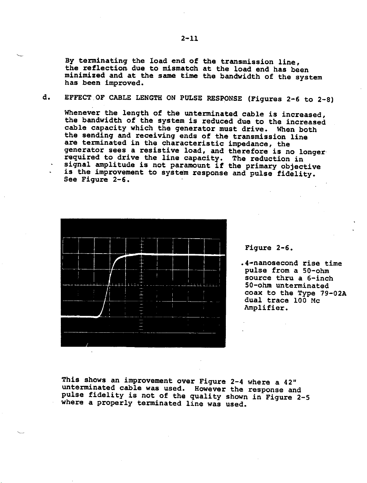
Figure 2-6.
.
{-nanosecond
pulse
Eource
50-ohtn
coax
dual
from
thru
unterminated
to the
trace
Amplifier.
to
both
line
longer
in
rise
a
50-ohm
a 6-inch
Type
100 Uc
2-8)
time
79-02A
This
unterminated
pulse
where
shows
fidelity
properly
a
an improvement
cable was
is not
terninated
over
used.
of
the
Figure
How6ver
guallty
line
wai
2-4
the
shown
used.
where
response
in
a 42"
Figure
and
2-5
2-L2
In
that- the
terminated
and
The
both ends
termlnated.
matching
determlned
of.mismatch-
In
three-nanosecond pulse
source
coaxial
positive
end
caused
The
than in
yse9:
in
Figures
fidelity,
previous
the
generator
in
load
the
pul6e
end
response will
of the
Reflections
and
the duration
by the length
illustrative
into
(scope
by
duration
The
different
cable
overshoot
input)
the mismatch
of the reflection
Figure
application
2-7
but
example, Figure
end
the characteristic
(scope
coaxial cable
examples,
to the Type
is due
and
2-8 due
and 2-8
at
the expense
2-6,
the
of
input)
be adversely
will
of
of
Figures
was coupled
lengths
79.-02A
to
coax
impedairce-
was
are
occur
the
reflection
cable
of unterminated
Amplifier.
the mismatch
the negative
at the
Eource
is
to the
longer
of minimurr
would
have
of
signal
lt was
was properly
unterminated.
affected
properly
not
due-
to the nis-
between
2-7
and
from
a 50-ohrn
reflection
generator
or
longer-
length
assumed
of ihe
will
the
2-9,
?he
at the
j.n
Flgure
of cable
line
when
be
poirts
a
7s-ohrr
load
is
end.
loss mitchlng pads
improved
pulie'
amplitude.
2-z
2-L3
Figure
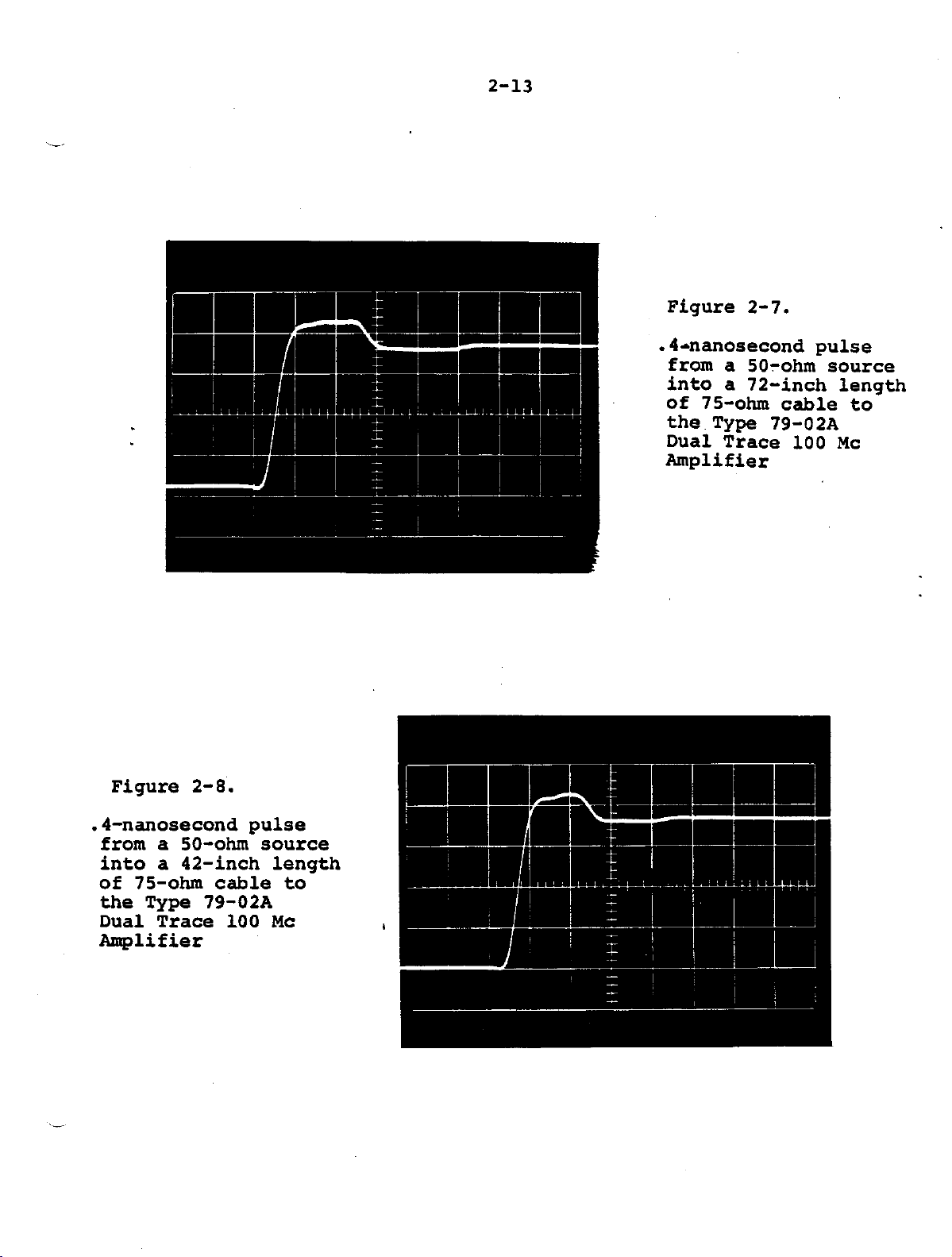
.4-nanosecond
from
into a
of 75-ohm
the rype
Dual
2-7.
a
50:ohm
72-inch
79-02A
Trace
cable
lO0
Anpllfler
pulse
source
length
to
Mc
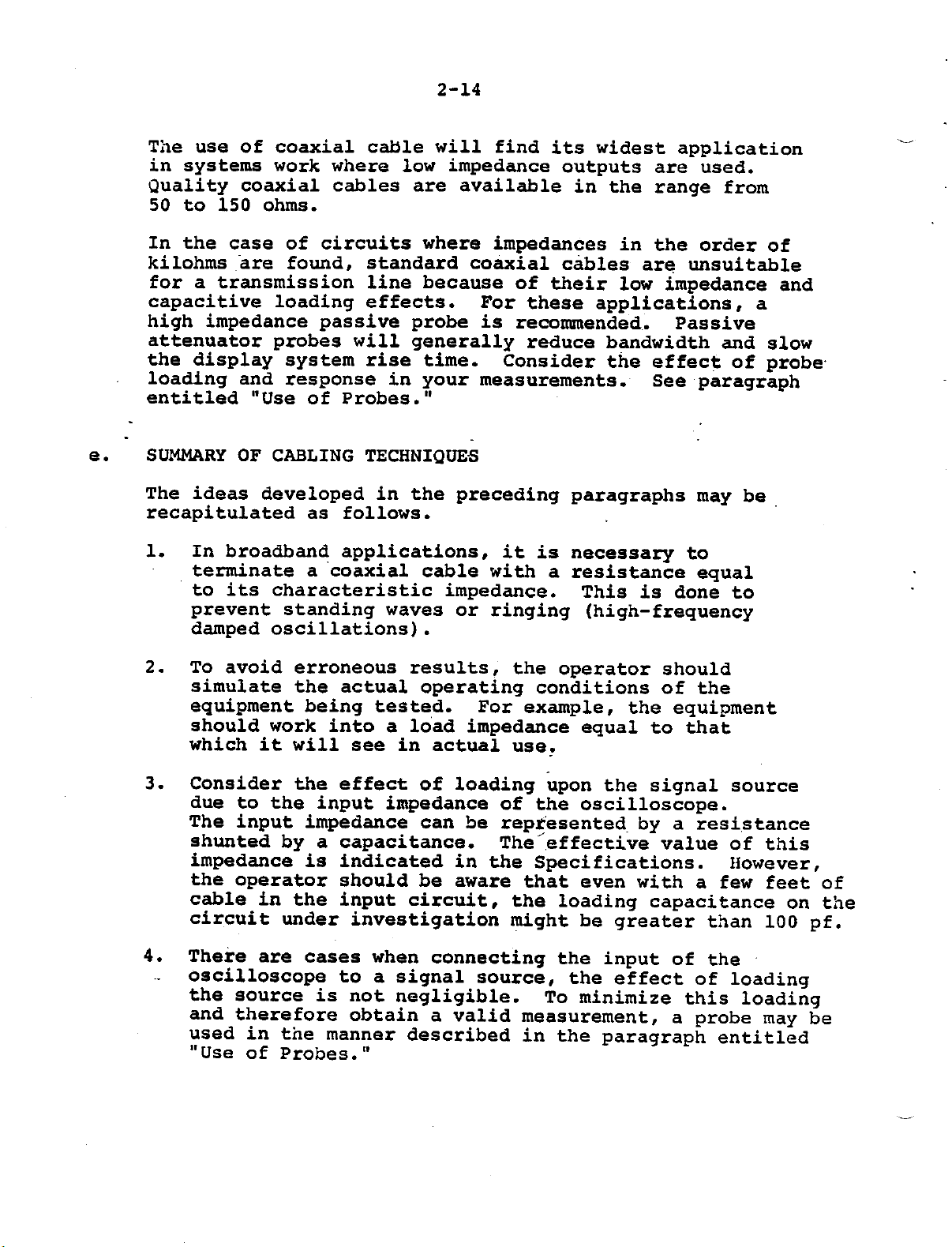
Flgure 2- 8.
.4-nanosecond
from
a
50-ohm source
pulse
into a 42-inch length
of 75-ohn cable to
the Type 79-02A
Dual Trace 100 Mc
Arylifier
2-L4
The
use of coaxial cable lrill find
in systems
Quality
50
to 150 otuns.
work
where
low
coaxial cables are available
inpedance
widest
its
outputs
in
the range
application
are used.
from
In the
kilohms are
for
case of circuits
found, standard
a transmission line
capacitive loading
high impedance
attenuator
display
lhe
Ioadlng
entitled
SUMMARY OT'
The ideas
and
"Use
developed in the
recapitulated
In
I.
broadband
passive probe
probes
system rise
response in
of ProbeE.
CABLING TECHNIOT'ES
as follows.
applicatlons,
terminate a coaxial
to its characteristic
prevent
danped
2. To
avoid
Eimulate
equipment being
should rdork
whi.ch
standing waves
oscillations).
erroneous results,
the actual
into
it will
where
imped.rnces
coaxial
because
effects. for
i.s
will
generally
time. Consider
your
"
cable with
operating
measurements.
precedlng
impedance.
or
ringing
tested. For
a load impedance
see in actual
in
the order
cables
of
their
these applications,
reclomttended..
reduce bandwidth
are unsuitable
lolr irnpedance
passive
the effect of
See
paragraphs
it
the
use.
necessary
is
a
resLstance
This
(high-frequency
is done
operator should
conditions
example,
the equipment
equal
to
of the
to that
of
and
a
and
slow
probe
paragraph
may
be
equal
to
3. Consider
due
to the input
The
cable
input
shunted
impedance
the
operator
in
circuit
4. Theie
,
oscllloscope
the source
and
used
"Use
are
therefore
in the
of Probes.
the effect
impedance
of loading
impedance
can be
by a capacitance.
is indicated
should be aware
in the
the input circuit,
under
investigation
cases when
to
a signal
is not
negligible.
obtain
manner
described
"
connecting
source,
a valid
upon the
of
the oscilloscope.
represented.
by a
The-effective
Specifications.
that even with
the loading
might
the input
To minimize
measurementr
in the
gieat-r
be
the
eifect
paragraph
signal source
resistance
value
capacitance
of
of this
However,
a
few feet of
than
the
IOO
of 1oading
this
a
loading
probe
may
entitl;d
on the
pf.
be
2-1.5
f.
5. Care
rise,
connector.
properly
the signal
the rising
will
CABLING FOR RACK-MOT'NTING
For
rack-mounlilrg systemg.
precautions
It
1.
only at one
microa.mperes
braid can cauEe
2.
Use cable with
so
3. Use
where
must
be
exercised
high-fregugncy
It
terminate
to
and falling
result.
if long, shielded
may be
desirable
end to.
of
that
the cable does
off-ground
applicable.
lrill
be
the
the oscilloscope
to
avoid
extraneous
unrranted
insulation
insulated
when
signal
necessary
coaxial
applying
to tle input
to rnltch
cable
or ringing
portion
SYSTEI,{S
observe
cables are
ground
of
the-waveform
the following
long
shielded
circulation
currentE
distortions.
over
not accidentally
bulkhead
the shielded
feed-thru
a
fast
and
applying
on-
used.
-
leads
currents.
in
the
shielded
braid
touch ground.
connectors
Even
4. Do
not
5. Long-
oscillations.
1000-ohm,
erith
input
6. Use
a
just
value
pass
shielded
cables
input
It
L/2 w atL
the
center
terminals.
reEistance at
stop
may
the
reduce
conductor
parasitic
near
is
resistor
strong
cables
suggested
may
near
be
least'tlrice
oscillationg.
the bandwidth
AC
magnetic
also
that
connected
or at
induce
a l00-ohm
that
the oscilloscope
required
ioo
of the
system.
fields.
parasitic.
to
in
series
to
large
a
2-16
2- 8. USE
a.
OF PROBES
INTRODUSrION
An attenuator probe
resistive
Simultaneously, whl1e
loading cauEed
reduces
by
isolating
the signal source, it reduces
of the
form
factor
When
matched,
may
necessary
circuit
adj
ustments are completed,
precisely
be added
instrument.
will
using
be reduced in amplitude
the
probe
probe
of the
or othenrise
cause erroneous
to renove capacity
under
observatlon.
equal to that
to the circuit
the circuit. This
restore
under observation
neagurementg were
the operating characteristics
In
other
.
to sample
critical
readings.
capacitance
of
the
after
substitutj.on
to
the same
made.
both
the
the capacitive
oscilloscope.
the oscilloscope
the effective
r^rords,
the displayed
by the
signals
circuit,
In
these cases
and
resistance.
When
the observations
probe
the
will
impedance,
probe
equalize
of the
conditions
and
from
sensitivity
wave-
attenuation
from
and resistance
a tuned,
capactive
it
may
from
thL
should
is removed
loads
and
from
loading and
circuit
as when probe
be
b.
When
neasurements,
display
TYPE
As
the
there will
loading
characteristics
resistance
The
high-freguency probe
the Type
low-
oscilloscope
when
reactive
using the attenuator probe
multiply
by the attenuation
79948 PROBE
is
the case rrhere
over-alI system
be a certain
introduced by
of the circuit
and capacitance
Fairchil.al
79-02A
frequencies,
usin!
components
Type 79948
100 Mc Amplifier
the
appears
probe
the
factors.
Since
such
that
probe
the
no reflections
is used
to make amplitude
tha
observed
factor
probe
any
bandwidth .and
degree
probe
the
of the
Probe
which
has been
marked
is used
response is
of
loading.
will
under
probe.
is basically
plug-in
probe
as a compensated
to monitor
and
together
nanosecond pulses,
line
unterminated,
or
losses
ringing will
amplitude
on the
with an
The
be
determined
test and
an
designed
as a system.
;ith
the
divider.
become
the
important
design
occur
of the
probe.
oscilloscope,
reduced
amount
by the
the input
unterminated
wo work
input
However,
of the
the
must
with
be
to cause
and-
of
At
2-L7
c.
signal
center
critical
cable
capacitance,
be
carefully
d;imped. In
deterioration.
conductor
factor
is
unterminated
used as
a center
selected
the Pairchlld
it is necessary
is a termination
probe.
the
resistive
resPonse
There
9.an Pe
966
maintain
Eairchild
input
will
the Type
EFPECT
(Figures
is
ysgg
6,i.dwidth
impedance
provide
OF
This
components
at
high
a limitation
ln
of
the B ame
Type
a 78 Mc
79-02A
PROBE
2-9
to 2-11)
The
at high
in the
network
network
frequencies.
probe
the
system,
probe
and
conductor.
so
that
and
as
input
79948 Ls
of 10
Dual Trace
GROUND
negohms
system
LEAD
lead
frequencies
j.nductance
design.
has
inductance
that
,This
the
cable
Type
located
consists
is
to
lrlthout
assuning
impedance
a 3-L/Z
l0O Mc
29948
used
the
lenqth
severely
foot
and 7
bandwidtl
ON PULSE
becomes
Since
and
a
resistance
resistance
is critically
probe,
at
the scope
of reactlve
to
adjust
the
of cable
restricting
that wE
in
the
probi
picofarads
when
Amplifier.
RESPONSE
desire
probe.
with
used with
of
a
the
there
the
wire
is
end
and
that
to
?he
an
which
of
-
The
most
frequency probe
ringing
lead.
rise pulses,
be
employed.
reEponse
in
Figures
reson.rnt
of
the
It
is obvious
response
to
improper grounding
globe and
linitatlons
on
the oseilloscope.
common
due to.the
When
using
a
See
is
shown
2-9 and
circuit
probe
input
fron
and bandwldth
an understanding
will
problem
is
the introduction
use
encountered
of
an
the Type
gronnd
t'igures
lead
2-9
ln Figure
2-10
made
capacity.
the
insure
is
up
of
foregoing
can
of
the
the
excessively
29948
as
2-11.
due
the
probe
short
to
2-11.
The
to
excitati6n
ground
that
greatl!
be
piobe.
of
its
capabilities
display
when
using
a high-
of high-fiequen6y
iong
io moii[,or
as possible
-
Optimum pulse
riiging
giouna'
fast-
should
oLserved
6f a
lead
the
exag-gerated
Correct
-of
true
inductance
pulse
use
of
and
information
due
the
2-L8
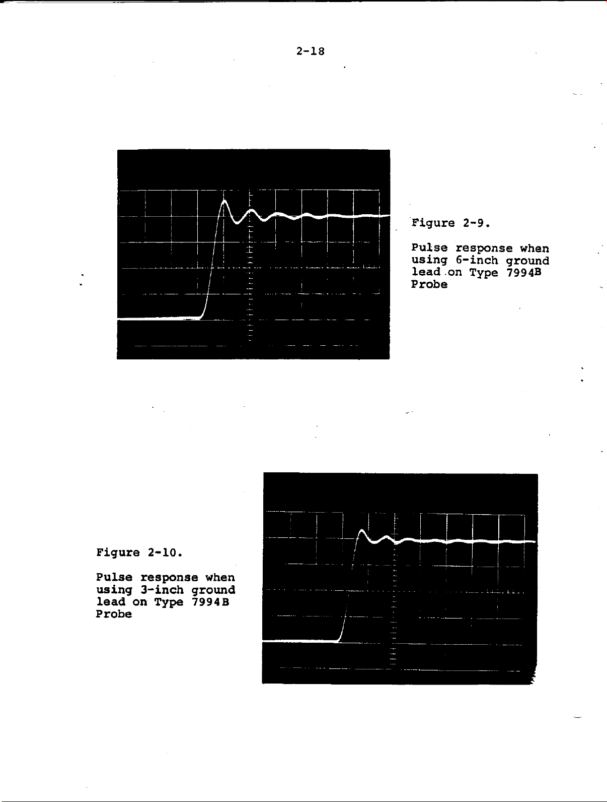
Flgure
Pulse
2-9.
response
using 6-inch
lead.on
Probe
fype
when
ground
79948
Flgure
Pulse
2-10.
response rrhen
using 3-inch
Lead
Probe
on Type
ground
79948
 Loading...