

Fairchild 74AC10 service manual
查询74AC10供应商
74AC10 • 74ACT10
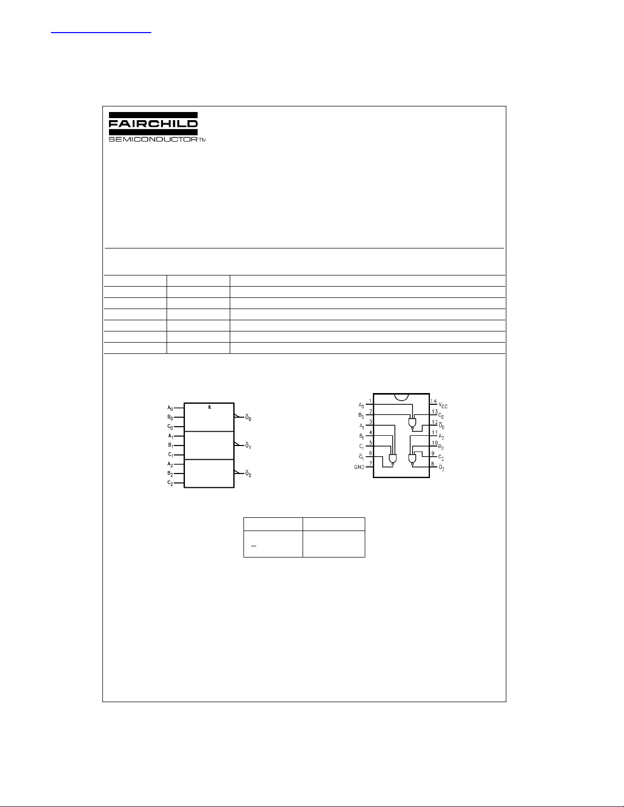
Triple 3-Input NAND Gate
74AC10 • 74ACT10 Triple 3-Input NAND Gate
November 1988
Revised January 2000
General Description
The AC/ACT10 contains three, 3-input NAND gates.
Features
■ ICC reduced by 50% on 74AC only
■ Outputs source/sink 24 mA
Ordering Code:
Order Number Package Number Package Description
74AC10SC M14A 14-Lead Small Outline Integrated Circuit (SOIC), JEDEC MS-120, 0.150” Narrow Body
74AC10SJ M14D 14-Lead Small Outline Package (SOP), EIAJ TYPE II, 5.3mm Wide
74AC10MTC MTC14 14-Lead Thin Shrink Small Outline Package (TSSOP), JEDEC MO-153, 4.4mm Wide
74AC10PC N14A 14-Lead Plastic Dual-In-Line Package (PDIP), JEDEC MS-001, 0.300” Wide
74ACT10SC M14A 14- Le a d Sm al l Ou tl i ne In te gr at e d C ir c uit ( S OIC ) , JE DE C MS - 12 0 , 0. 15 0” N ar r ow B ody
74ACT10PC N14A 14-Lead Plastic Dual-In-Line Package (PDIP), JEDEC MS-001, 0.300” Wide
Device also available in Tape and Reel. Specify by appending s uffix let te r “X” to the ordering code .
Logic Symbol
IEEE/IEC
Connection Diagram
Pin Descriptions
Pin Names Description
, Bn, C
A
n
O
n
© 2000 Fairchild Semiconductor Corporation DS009915 www.fairchildsemi.com
Inputs
n
Outputs
Absolute Maximum Ratings(Note 1) Recommended Operating
Supply Voltage (VCC) −0.5V to +7.0V
DC Input Diode Current (I
= −0.5V −20 mA
V
I
= VCC + 0.5V +20 mA
V
I
DC Input Voltage (V
DC Output Diode Current (I
= −0.5V −20 mA
V
74AC10 • 74ACT10
O
= VCC + 0.5V +20 mA
V
O
DC Output Voltage (V
)
IK
) −0.5V to VCC + 0.5V
I
)
OK
) −0.5V to VCC + 0.5V
O
DC Output Source
or Sink Current (I
or Ground Current
DC V
CC
per Output Pin (I
Storage Temperature (T
Junction Temperature (T
) ± 50 mA
O
or I
CC
) ± 50 mA
GND
) −65°C to +150°C
STG
)
J
PDIP 140°C
Conditions
Supply Voltage (V
AC 2.0V to 6.0V
ACT 4.5V to 5.5V
Input Voltage (V
Output Voltage (VO) 0V to V
Operating Temperature (TA) −40°C to +85°C
Minimum Input Edge Rate (∆V/∆t)
AC Devices
from 30% to 70% of V
V
IN
VCC @ 3.3V, 4.5V, 5.5V 125 mV/ns
Minimum Input Edge Rate (∆V/∆t)
ACT Devices
from 0.8V to 2.0V
V
IN
@ 4.5V, 5.5V 125 mV/ns
V
CC
Note 1: Absolute maximum ratings are those values beyond which damage
to the device may occur. The databook specifications should be met, without exception, to ensure that the system design is reliable over its pow er
supply, temperature, and ou tput/inp ut loadi ng varia bles. Fairchild does no t
recommend operat ion of circuits outside d at abook specifications .
)
CC
) 0V to V
I
CC
DC Electrical Characteristics for AC
V
Symbol Parameter
V
V
V
V
I
IN
(Note 4) Leakage Current or GND
I
OLD
I
OHD
I
CC
(Note 4) Supply Current or GND
Note 2: All outputs loaded; thresholds on input associated wit h output under test.
Note 3: Maximum te st duration 2.0 ms, one ou t put loaded at a time.
Note 4: I
Minimum HIGH Level 3.0 1.5 2.1 2.1 V
IH
Input Voltage 4.5 2.25 3.15 3.15 V or VCC − 0.1V
Maximum LOW Level 3.0 1.5 0.9 0.9 V
IL
Input Voltage 4.5 2.25 1.35 1.35 V or VCC − 0.1V
Minimum HIGH Level 3.0 2.99 2.9 2.9
OH
Output Voltage 4.5 4.49 4.4 4.4 V I
Maximum LOW Level 3.0 0.002 0.1 0.1
OL
Output Voltage 4.5 0.001 0.1 0.1 V I
Maximum Input
Minimum Dynamic 5.5 75 mA V
Output Current (Note 3) 5.5 −75 mA V
Maximum Quiescent
and ICC @ 3.0V are guaranteed to be less than or equal to the respective limit @ 5. 5V VCC.
IN
CC
(V) Typ Guaranteed Limi ts
5.5 2.75 3.85 3.85
5.5 2.75 1.65 1.65
5.55.495.4 5.4
3.0 2.56 2.46 IOH = −12 mA
4.5 3.86 3.76 V IOH = −24 mA
5.5 4.86 4.76 IOH = −24 mA (Note 2)
5.5 0.001 0.1 0.1
3.0 0.36 0.44 IOL = 12 mA
4.5 0.36 0.44 V IOL = 24 mA
5.5 0.36 0.44 IOL = 24 mA (Note 2)
5.5 ±0.1 ±1.0 µA
5.5 2.0 20.0 µA
TA = +25°C
TA = −40°C to +85°C
Units Conditions
= 0.1V
OUT
= 0.1V
OUT
= −50 µA
OUT
VIN = VILor V
= 50 µA
OUT
VIN = VIL or V
VI = V
CC
= 1.65V Max
OLD
= 3.85V Min
OHD
VIN = V
CC
CC
CC
IH
IH
www.fairchildsemi.com 2
DC Electrical Characteristics for ACT
V
Symbol Parameter
V
Minimum HIGH Level 4.5 1.5 2.0 2.0
IH
CC
(V) Typ Guaranteed Limits
Input Voltage 5.5 1.5 2.0 2.0 or VCC − 0.1V
V
Maximum LOW Level 4.5 1.5 0.8 0.8
IL
Input Voltage 5.5 1.5 0.8 0.8 or VCC − 0.1V
V
Minimum HIGH Level 4.5 4.49 4.4 4.4
OH
Output Voltage 5.5 5.49 5.4 5.4
4.5 3.86 3.76 V IOH= −24 mA
5.5 4.86 4.76 IOH = −24 mA (Note 5)
V
Maximum LOW Level 4.5 0.001 0.1 0.1
OL
Output Voltage 5.5 0.001 0.1 0.1
4.5 0.36 0.44 V IOL = 24 mA
5.5 0.36 0.44 IOL = 24 mA (Note 5)
I
IN
I
CCT
I
OLD
I
OHD
I
CC
Note 5: All outputs loaded; thresholds on input associated with ou t put under test.
Note 6: Maximum test duration 2.0 ms, one output loaded at a time.
Maximum Input
Leakage Current
Maximum
ICC/Input
5.5 ±0.1 ±1.0 µAVI = VCC, GND
5.5 0.6 1.5 mA VI = VCC − 2.1V
Minimum Dynamic 5.5 75 mA V
Output Current (Note 6) 5.5 −75 mA V
Maximum Quiescent
Supply Current or GND
5.5 4.0 40.0 µA
TA = +25°C
TA = −40°C to +85°C
Units Conditions
V
= 0.1V
OUT
V
V
= 0.1V
OUT
V
VI
VI
= −50 µA
OUT
VIN = VILor V
= 50 µA
OUT
VIN = VIL or V
= 1.65V Max
OLD
= 3.85V Min
OHD
VIN = V
CC
IH
IH
74AC10 • 74ACT10
AC Electrical Characteristics for AC
Symbol Parameter
t
PLH
t
PHL
Note 7: Voltage Range 3.3 is 3.3V ± 0.3V
Propagation Delay 3.3 1.5 6.0 9.5 1.0 10.5
Propagation Delay 3.3 1.5 5.5 8.5 1.0 10.0
Voltage Range 5.0 is 5.0V ± 0.5V
V
CC
(V)
(Note 7) Min Typ Max Min Max
5.0 1.5 4.5 7.0 1.0 8.0
5.0 1.5 4.0 6.0 1.0 6.5
TA = +25°CT
= −40°C to +85°C
A
CL = 50 pF CL = 50 pF
AC Electrical Characteristics for ACT
Symbol Parameter
t
PLH
t
PHL
Note 8: Voltage Range 5.0 is 5.0V ± 0.5V
Propagation Delay 5.0 1.0 6.5 9.0 1.0 10.0 n s
Propagation Delay 5.0 1.0 6.5 9.0 1.0 9.5 ns
V
CC
(V)
TA = +25°C
CL = 50 pF CL = 50 pF
(Note 8) Min Typ Max Min Max
TA = −40°C to +85°C
Capacitance
Symbol Parameter Typ Units Conditions
C
IN
C
PD
Input Capacitance 4.5 pF VCC = OPEN
Power Dissipation Capacitance 25.0 pF VCC = 5.0V
Units
ns
ns
Units
3 www.fairchildsemi.com
 Loading...