Fairchild 74ABT16652 service manual

查询74ABT16652供应商
74ABT16652
16-Bit Transceivers and Registers with 3-STATE Outputs
74ABT16652 16-Bit Transceivers and Registers with 3-STATE Outputs
April 1993
Revised January 1999
General Description
The ABT16652 consist s of sixteen bus transce iver circuits
with D-type flip-flops, and control circuitry arranged for multiplexed transmission of data directly fro m the input bus or
from the interna l registers. Each byte has separate control
inputs which can be sho rted toge ther for full 16-bit operation. Data on the A or B bus will be clocked into the registers as the appropr iate clock pin goes to HI GH logic level.
Output Enable pins (OEAB, OEBA
the transceiver function.
) are provided to control
Features
■ Independent registers for A and B buses
■ Multiplexed real-time and stored data
■ Separate control logic for each byte
■ A and B output sink capability of 64 mA, source
capability of 32 mA
■ Guaranteed output skew
■ High impedance glitch free bus loading during entire
power up and power down cycle
■ Nondestructive hot insertion capability
Ordering Code:
Order Number Package Number Package Description
74ABT16652CSSC MS56A 56-Lead Shrink Small Outline Package (SSOP), JEDEC MO-118, 0.300” Wide
74ABT16652CMTD MTD56 56-Lead Thin Shrink Small Outline Package (TSSOP), JEDEC MO-153, 6.1mm Wide
Devices also available in Tape and Reel. Specify by appending the suffix letter “X” t o t he ordering code.
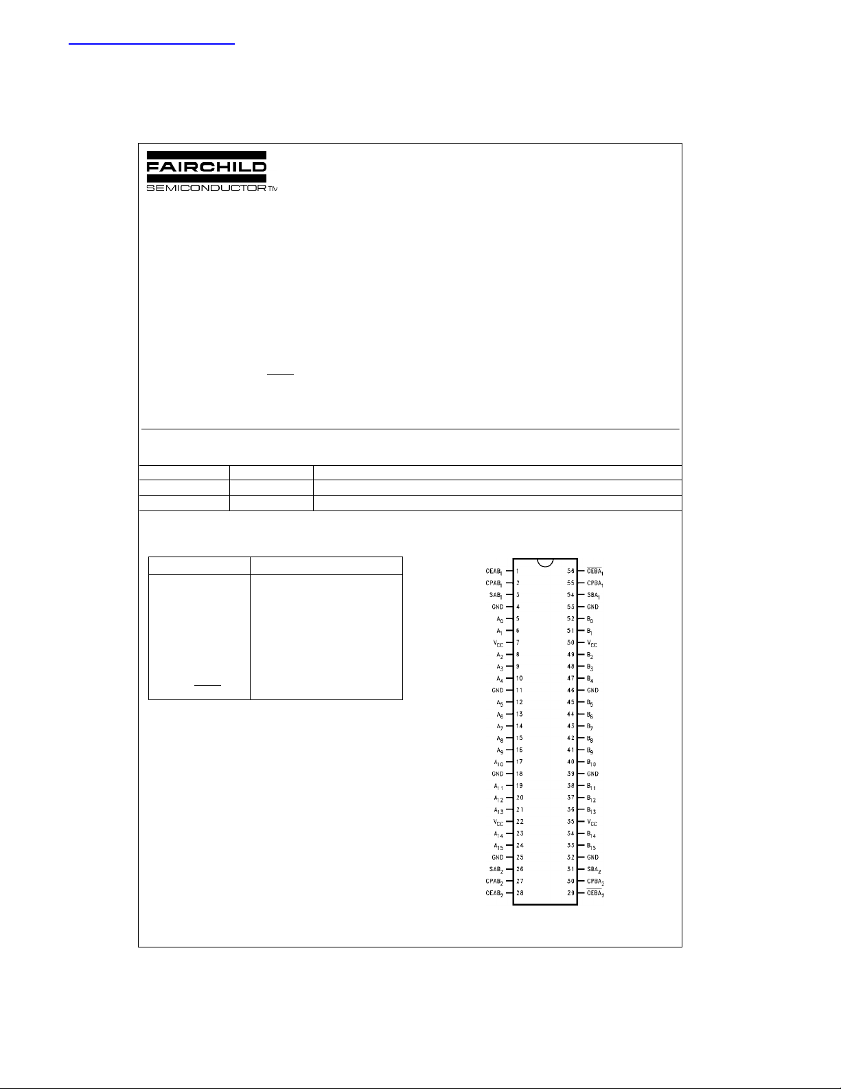
Pin Descriptions Connection Diagram
Pin Names Descriptions
A
0–A16
B
0–B16
CPAB
SAB
OEAB
, CPBA
n
, SBA
n
n
n
, OEBA
Data Register A Inputs/
3-STATE Outputs
Data Register B Inputs/
3-STATE Outputs
Clock Pulse Inputs
n
Select Inputs
Output Enable Inputs
n
© 1999 Fairchild Semiconductor Corporation DS011599.prf www.fairchildsemi.com

Functional Description
In the transceiver mo de, data presen t at the HI GH impedance port may be stored in either the A or B register or
both.
The select (SAB
real-time.
74ABT16652
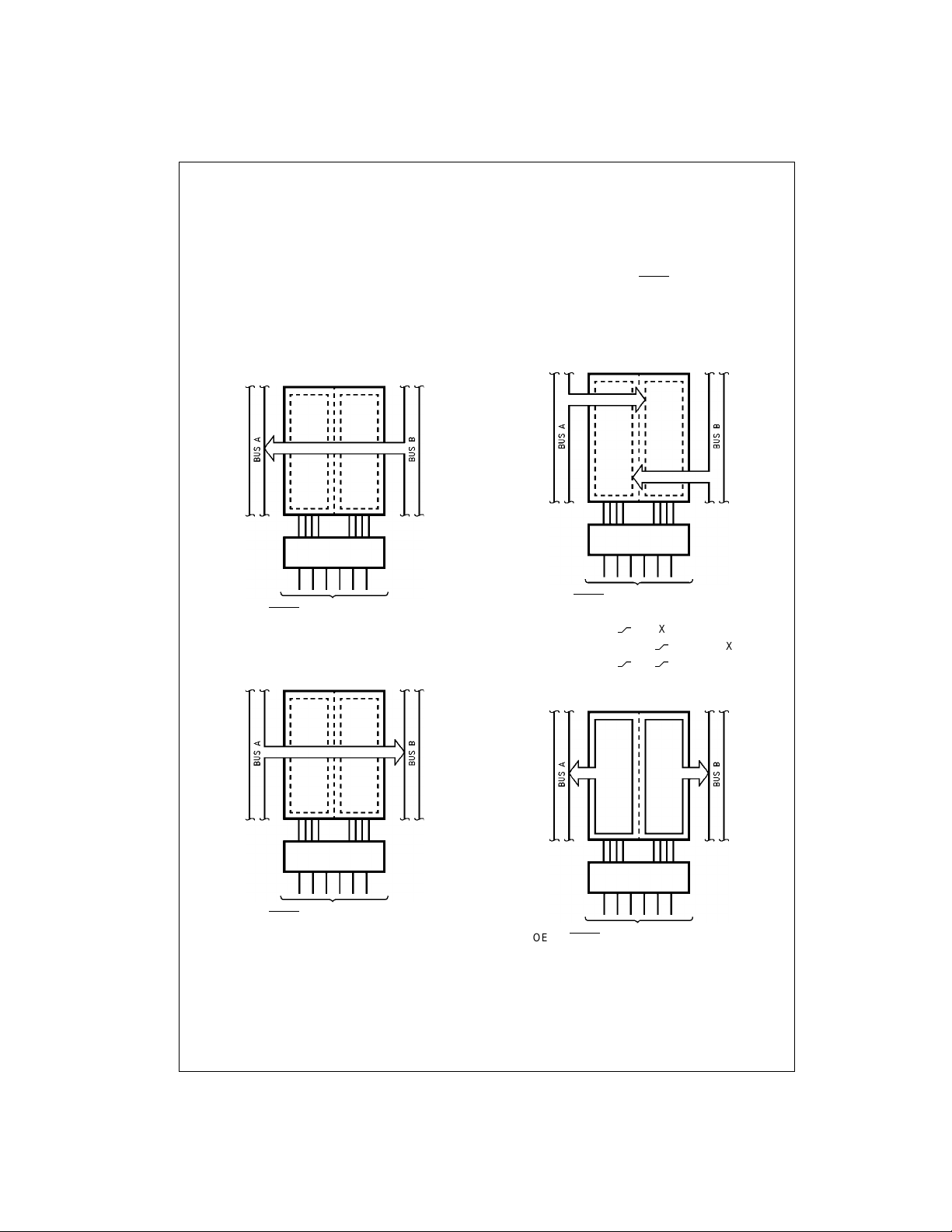
The examples in
tal bus-management fun ctions that can be perfor med with
the ABT16652.
, SBAn) controls can multiplex stored and
n
Figure 1
demonstrate the four fundamen -
Data on the A or B data bus, or bot h can be stor ed in the
internal D flip-flop by LOW to HIGH transitions at the
appropriate Clock Inputs (CPAB
, CPBAn) regardless of
n
the Select or Output Enable Inputs. When SAB and SBA
are in the real time transfer mode, it is also possible to
store data without using the internal D flip-flops by simultaneously enabling OE AB
and OEBAn. In this configuration
n
each Output reinforces it s Input. Thu s when a ll other data
sources to the two sets of bus lines are i n a HIGH impedance state, each set of bus lines will remain at its last state.
Note A: Real-Time
Transfer Bus B to Bus A
OEBA1CPAB1CPBA1SAB1SBA
OEAB
1
LLXXXL
Note B: Real-Time
Transfer Bus A to Bus B
Note C: Storage
OEAB1OEBA1CPAB1CPBA1SAB1SBA
1
XH
LXX
LH
XXX
1
XX
XX
Note D: Transfer Storage
Data to A or B
OEBA1CPAB1CPBA1SAB1SBA
OEAB
1
1
HHXXLX
FIGURE 1.
www.fairchildsemi.com 2
OEBA1CPAB1CPBA1SAB1SBA
OEAB
1
H L H or L H or L H H
1

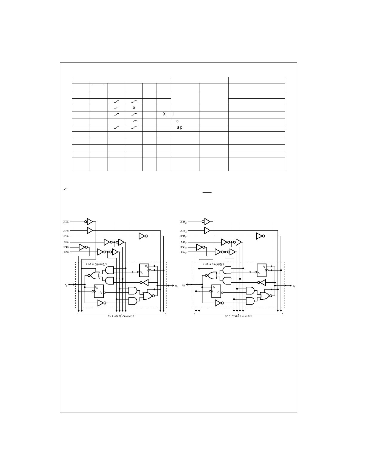
Function Table
Inputs Inputs/Outputs (Note 1) Operating Mode
OEBA1 CPAB1 CPBA1 SAB1 SBA1 A0 thru A7 B0 thru B
OEAB
1
7
L H H or L H or L X X Input Input Isolation
L H
X H
H H
L X H or L
L L
H or L X X Input Not Specified Store A, Hold B
X X Store A and B Data
X X Input Output Store A in Both Registers
X X Not Specified Input Hold A, Store B
X X Output Input Store B in Both Registers
L L X X X L Output Input Real-Time B Data to A Bus
L L X H or L X H Store B Data to A Bus
H H X X L X
H H H or L X H X Stored A Data to B Bus
Input Output
Real-Time A Data to B Bus
H L H or L H or L H H Output Output Stored A Data to B Bus and
Stored B Data to A Bus
H = HIGH Voltage Level
L = LOW Voltage Level
X = Immaterial
= LOW to HIGH Clock Transition
Note 1: The data ou tput fu nctions may be en abled o r disabled by various sign als at OEAB or O EBA
data at the bus pins will be sto red on every LOW to HIGH transit ion on the clock inputs. This also applies to data I/O (A and B: 8–15) and #2 con tr ol pins.
inputs. Data inpu t fun ctions are always e nabled, i.e.,
Logic Diagrams
74ABT16652
Please note that thes e diagrams are provided only for the understanding of lo gic operations and should not be used to estimat e propagation delays.
3 www.fairchildsemi.com
 Loading...