Fairchild 74ABT16501 service manual

查询74ABT16501供应商
74ABT16501
18-Bit Universal Bus Transceivers with 3-STATE Outputs
74ABT16501 18-Bit Universal Bus Transceivers with 3-STATE Outputs
January 1995
Revised January 1999
General Description
The ABT16501 18-bit u niversal bus transceiver combines
D-type latches and D-type flip-flops to allow data flow in
transparent, latched, and clocked modes.
Data flow in each direction is contr olled by output-enable
(OEAB and OEBA
clock (CLKAB and CLKBA) inputs. F or A- to-B data flo w, the
device operates in the transparent mode when LEAB is
HIGH. When LEAB is LOW, the A data is latched if CLKAB
is held at a HIGH or LO W logic level. If LEAB is LOW, the A
bus data is stored in the latch/flip-flop on the LOW-to-HIGH
transition of CLKAB. Output-enable OEAB is active-high.
When OEAB is HIGH, the outputs are active. When OEAB
is LOW, the outputs are in the high-impedance state.
Data flow for B to A is similar to tha t of A to B but uses
, LEBA, and CL KBA. The output enables are com-
OEBA
), latch-enable (LEA B and LEBA), and
plementary (OEAB is active HIGH and OEBA
LOW).
To ensure the high-imp edance state during power up or
power down, OE inputs should be tied to GND through a
pulldown resistor; the minimum value of the resistor is
determined by the current-sourcing capability of the driver.
Features
■ Combines D-Type latches and D-Type flip-flops for operation in transparent, latched, or clocked mode
■ Flow-through architecture optimizes PCB layout
■ Guaranteed latch-up protection
■ High impedance glitch free bus loading during entire
power up and power down cycle
■ Non-destructive hot insertion capability
is active
Ordering Code:
Order Number Package Number Package Description
74ABT16501CSSC MS56A 56-Lead Shrink Small Outline Package (SSOP), JEDEC MO-118, 0.300” Wide
74ABT16501CMTD MTD56 56-Lead Thin Shrink Small Outline Package (TSSOP), JEDEC MO-153, 6.1mm Wide
Devices also available in Tape or Reel. Specify by appending t he suffix letter “X” to the ordering code.
Connection Diagram
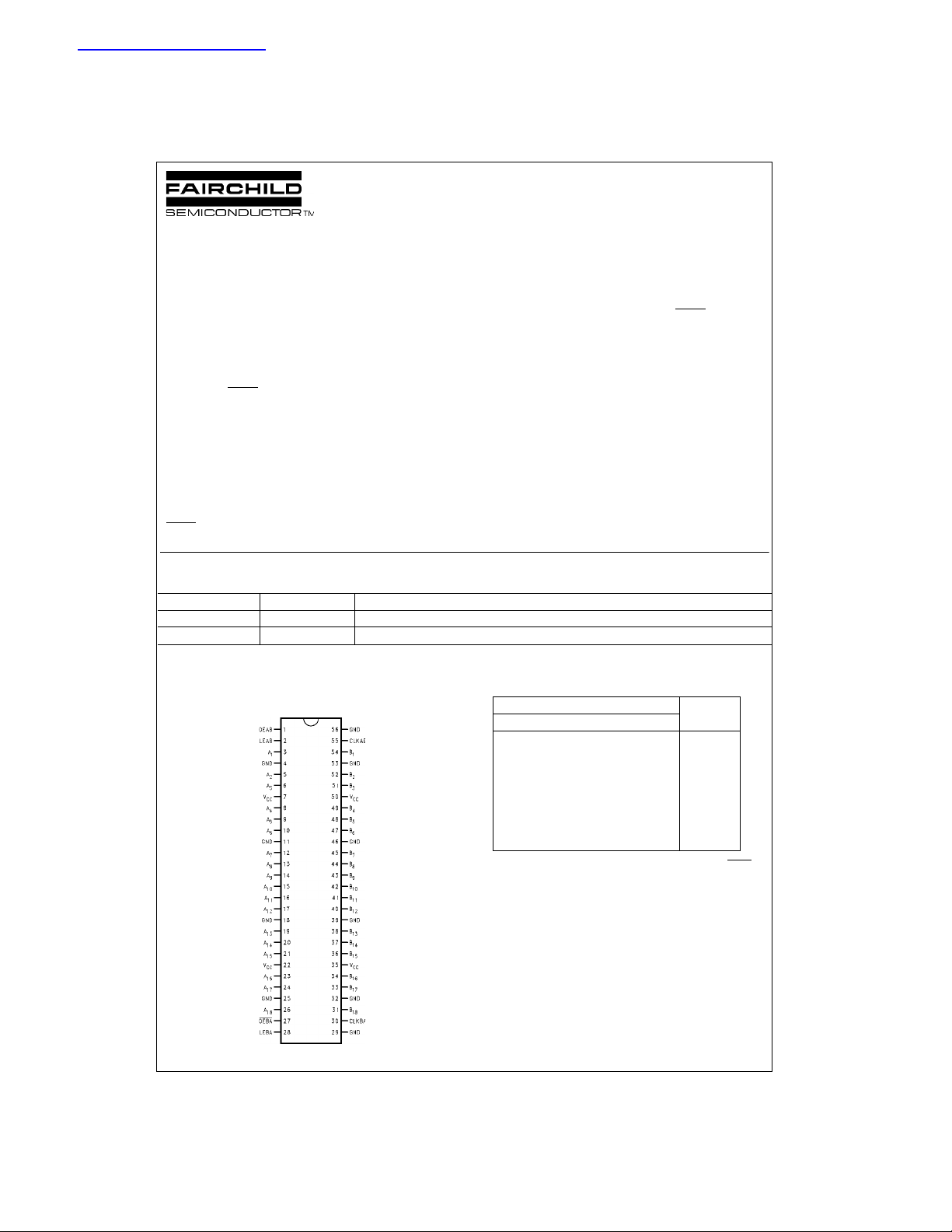
Pin Assign ment for SSOP
Function Table (Note 1)
Inputs Output
OEAB LEAB CLKAB A B
LXXX Z
HHXL L
HHXH H
HL↑ LL
HL↑ HH
HLHXB
HLLXB
Note 1: A-to-B data flow is s hown: B-to-A flow is similar but use s OEBA,
LEBA, and CLKBA.
Note 2: Output level before the indicated steady-state input conditions
were established.
Note 3: Output level before the indicated steady-state input conditions
were established, provided tha t CL KAB was HIGH before LEAB went LOW.
(Note 2)
0
(Note 3)
0
© 1999 Fairchild Semiconductor Corporation DS011690.prf www.fairchildsemi.com

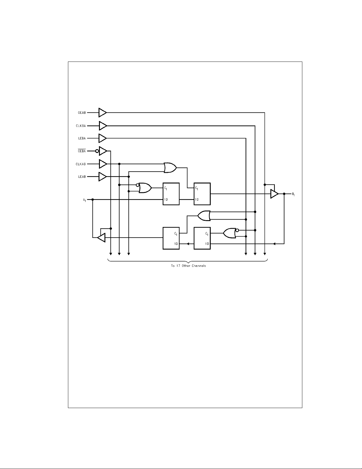
Logic Diagram
74ABT16501
www.fairchildsemi.com 2

Absolute Maximum Ratings(Note 4)
Storage Temperature −65°C to +150°C
Ambient Temperatur e under Bias −55°C to +125°C
Junction Temperature under Bias −55°C to +150°C
Pin Potential to
V
CC
Ground Pin −0.5V to +7.0V
Input Voltage (Note 5) −0.5V to +7.0V
Input Current (Note 5) −30 mA to +5.0 mA
Voltage Applied to Any Output
in the Disabled or
Power-off State −0.5V to 5.5V
in the HIGH State −0.5V to V
Current Applied to Output
in LOW State (Max) twice the rated I
OL
(mA)
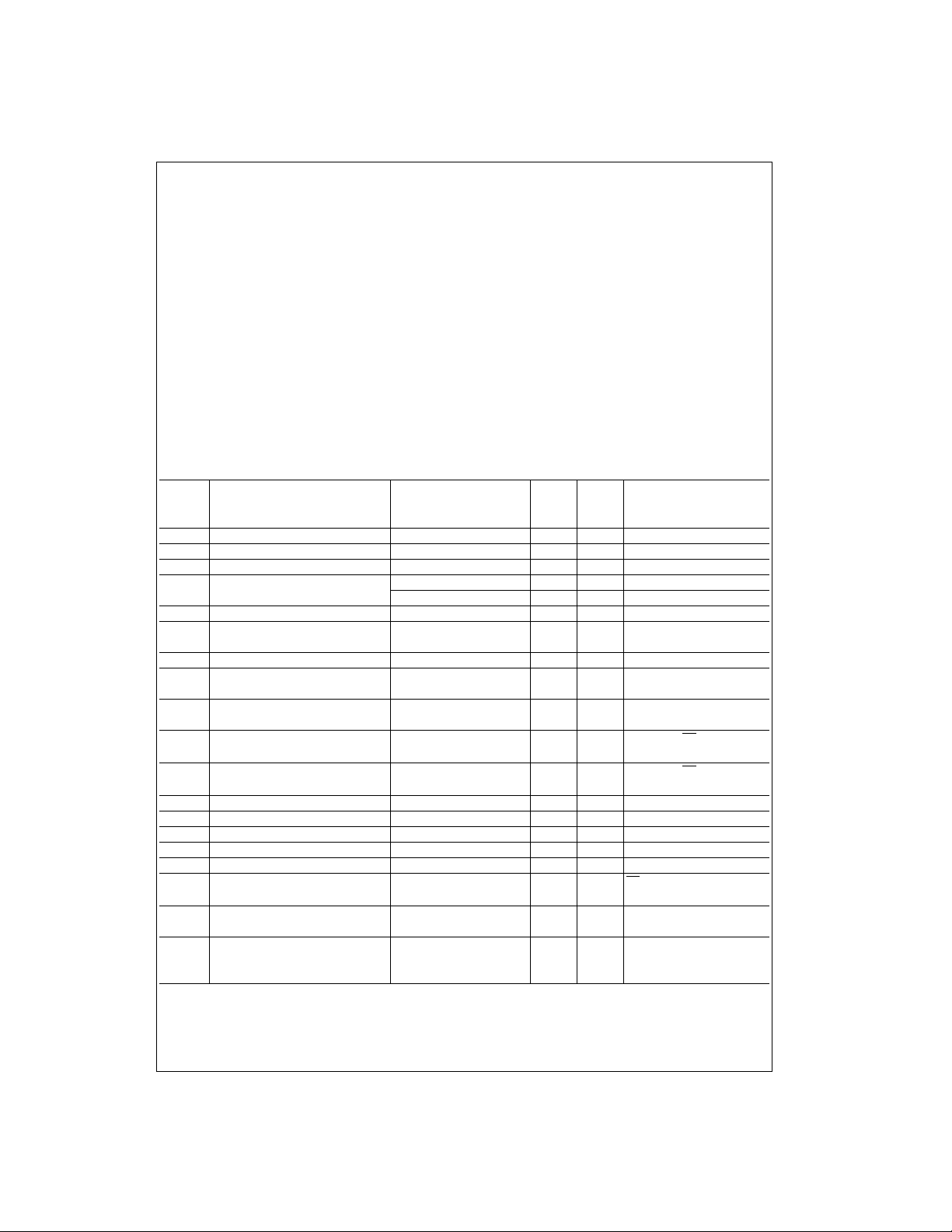
DC Electrical Characteristics
DC Latchup Source Current −500 mA
Over Voltage Latchup (I/O) 10V
Recommended Operating
Conditions
Free Air Ambient Temperature −40°C to +85°C
Supply Voltage +4.5V to +5.5V
Minimum Input Edge Rate (∆V/∆t)
Data Input 50 mV/ns
Enable Input 20 mV/ns
Note 4: Absolute maximum ratin gs are values beyond which the device
may be damaged or have its useful life impaired. Functional operation
under these condit ions is not implied.
CC
Note 5: Either voltage limit or current limi t is s uf f ic ient to protect inputs.
74ABT16501
Symbol Parameter Min Typ Max Units
V
V
V
V
V
I
I
I
V
IIH + Output Leakage Current
I
IIL + Output Leakage Current
I
I
I
I
I
I
I
I
I
Input HIGH Voltage 2.0 V Recognized HIGH Signal
IH
Input LOW Voltage 0.8 V Recognized LOW Signal
IL
Input Clamp Diode Voltage −1.2 V Min IIN = −18 mA
CD
Output HIGH Voltage 2.5 V Min IOH = −3 mA
OH
Output LOW Voltage 0.55 V Min IOL = 64 mA
OL
Input HIGH Current 1 µAMaxVIN = 2.7V (Note 6)
IH
Input HIGH Current Breakdown Test 7 µAMaxVIN = 7.0V
BVI
Input LOW Current −1 µAMaxVIN = 0.5V (Note 6)
IL
Input Leakage Test 4.75 V 0.0 IID = 1.9 µA
ID
OZH
OZL
Output Short-Circuit Current −100 −275 mA Max V
OS
Output HIGH Leakage Current 50 µAMaxV
CEX
Bus Drainage Test 100 µA0.0V
ZZ
Power Supply Current 1.0 mA Max All Outputs HIGH
CCH
Power Supply Current 68 mA Max An or Bn Outputs LOW
CCL
Power Supply Current
CCZ
Additional ICC/Input 2.5 mA Max VI = VCC − 2.1V
CCT
Dynamic I
CCD
Note 6: Guaranteed, but not tested.
CC
(Note 6) 0.23 MHz Transparent Mode
No Load mA/ Max Outputs Open
2.0 V Min IOH = −32 mA
1V
−1V
10 µA0 − 5.5V
−10 µA0 − 5.5V
1.0 mA Max
V
CC
Conditions
= V
IN
CC
= 0.0V
IN
All Other Pins Grounded
V
= 2.7V; OE, OE = 2.0V
OUT
V
= 0.5V; OE, OE = 2.0V
OUT
= 0V
OUT
= V
OUT
CC
= 5.5V; All Others GND
OUT
OEn = VCC,
All Others at VCC or GND
All Others at VCC or GND
One Bit Toggling, 50% Duty Cycle
3 www.fairchildsemi.com
 Loading...