

Fairchild 74ABT16245 service manual
查询74ABT16245供应商
74ABT16245
16-Bit Transceiver with 3-STATE Outputs
74ABT16245 16-Bit Transceiver with 3-STATE Outputs
April 1992
Revised May 2005
General Description
The ABT16245 c ontains si xteen non- inverti ng bidirecti onal
buffers with 3-STATE outputs and is intended for bus oriented applications. The device is byte controlled. Each
byte has separate control inputs which can be shorted
together for full 16-b it ope rat ion. T he T/ R
the direct i o n of d ata flow throug h t he d ev ic e . Th e OE
disable both the A and B ports by placing them in a high
impedance state.
inputs determine
inputs
Features
■ Bidirectional non-inverting buffers
■ Separate control logic for each byte
■ 16-bit version of the ABT245
■ A and B output sink capability of 64 mA, source
capability of 32 mA
■ Guaranteed output skew
■ Guaranteed multiple output switching specifications
■ Output switching specified for both 50 pF and
250 pF loads
■ Guaranteed simultaneous switching noise level and
dynamic threshold performance
■ Guaranteed latchup protection
■ High impedance glitch free bus loading during entire
power up and power down cycle
■ Non-destructive hot insertion capability
Ordering Code:
Order Number Package Number Package Description
74ABT16245CSSC MS48A 48-Lead Small Shrink Outline Package (SSOP), JEDEC MO-118, 0.300" Wide
74ABT16245CMTD MTD48 48-Lead Thin Shrink Small Outline Package (TSSOP), JEDEC MO-153, 6.1mm Wide
Device also availab le in Tape and Reel. Specify by appending suffix let te r “X” to the ordering code .
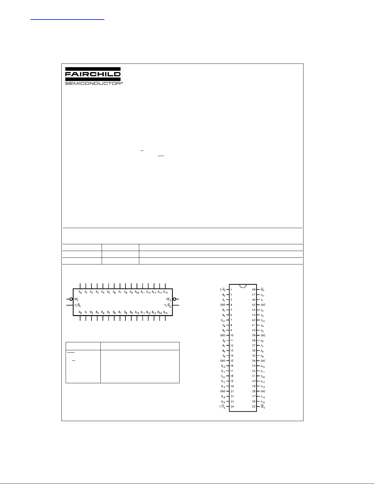
Logic Symbol
Connection Diagram
Pin Descriptions
Pin Names Description
OE
n
T/R
n
A
0–A15
B
0–B15
© 2005 Fairchild Semiconductor Corporation DS010986 www.fairchildsemi.com
Output Enable Input (Active LOW)
Transmit/Receive Input
Side A Inputs/Outputs
Side B Inputs/Outputs
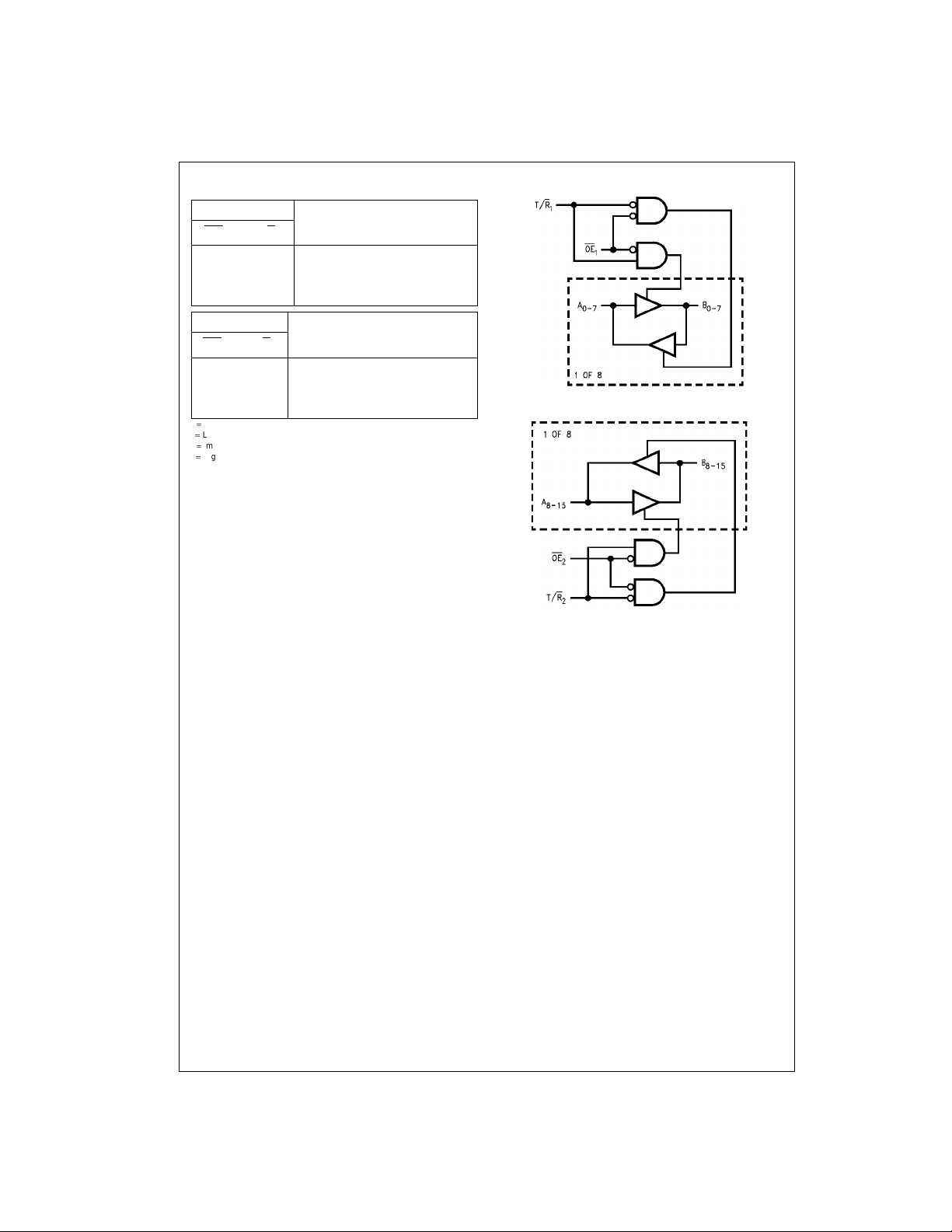
Truth Tables
Inputs Outputs
OE
74ABT16245
T/R
1
1
L L Bus B0–B7 Data to Bus A0–A
L H Bus A0–A7 Data to Bus B0–B
H X HIGH-Z State on A0–A7, B0–B
Inputs Outputs
OE
T/R
2
2
L L Bus B8–B15 Data to Bus A8–A
L H Bus A8–A15 Data to Bus B8–B
H X HIGH-Z State on A8–A15, B8–B
H HIGH Voltage Level
LOW Volt age Level
L
Immaterial
X
Z
High Impedance
Functional Description
The ABT16245 co ntains si xteen n on-i nverting bidire ction al
buffers with 3-STATE outputs. The device is byte controlled
with each byte funct ioning identically, but independent of
the other. The control pins can be shorted together to
obtain full 16-bit operation.
Logic Diagrams
7
7
7
15
15
15
www.fairchildsemi.com 2
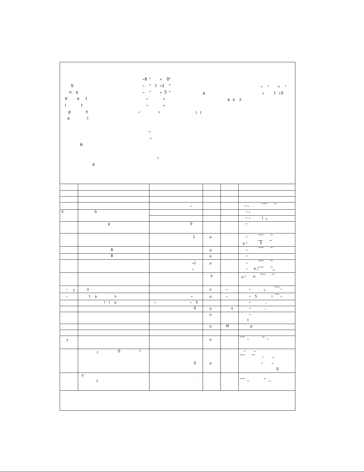
Absolute Maximum Ratings(Note 1) Recommended Operating
Storage Temperature
Ambient Temperature under Bias
Junction Temperature under Bias
Pin Potential to Ground Pin
V
CC
Input Voltage (Note 2)
Input Current (Note 2)
65q
C to 150qC
55q
C to 125qC
55q
C to 150qC
0.5V to 7.0V
0.5V to 7.0V
30 mA to 5.0 mA
Voltage Applied to Any Output
in the Disabled or
Power-Off State
in the HIGH State
0.5V to 5.5V
0.5V to V
Current Applied to Output
in LOW State (Max) twice the rated I
DC Latchup Source Current
OL
500 mA
Over Voltage Latchup (I/O) 10V
Conditions
Free Air Ambient Temperature
Supply Voltage
Minimum Input Edge Rate (
Data Input 50 mV/ns
Enable Input 20 mV/ns
CC
Note 1: Absolute maximum ratings are values beyond which the device
may be damaged or have its useful life impaired. Functional operation
(mA)
under these conditions is not implied.
Note 2: Either voltage limit or current limit is sufficient t o protect inputs.
'V/'
t)
DC Electrical Characteristics
Symbol Parameter Min Typ Max Units
V
Input HIGH Voltage 2.0 V Recognized HIGH Signal
IH
V
Input LOW Voltage 0.8 V Recognized LOW Signal
IL
V
Input Clamp Diode Voltage
CD
V
Output HIGH Voltage 2.5 V Min IOH 3 mA (An, Bn)
OH
V
Output LOW Voltage 0.55 V Min IOL 64 mA (An, Bn)
OL
2.0 V Min IOH 32 mA (An, Bn)
1.2 V Min IIN 18 mA (OEn, T/Rn)
V
CC
40q
C to 85qC
4.5V to 5.5V
Conditions
74ABT16245
I
Input HIGH Current 1
IH
I
Input HIGH Current Breakdown Test 7
BVI
I
Input HIGH Current Breakdown Test (I/O) 100
BVIT
I
Input LOW Current
IL
V
Input Leakage T est 4.75 V 0.0 IID 1.9 PA (OEn, T/Rn)
ID
I
I
Output Leakage Current 10
IH
OZH
IIL I
Output Leakage Current
OZL
Output Short-Circuit Current
I
OS
I
Output HIGH Leakage Current 50
CEX
I
Bus Drainage Test 100
ZZ
I
Power Supply Current 100
CCH
I
Power Supply Current 60 mA Max All Outputs LOW
CCL
I
Power Supply Current 100
CCZ
I
Additional ICC/Input Outputs Enabled 2.5 mA VI VCC 2.1V
CCT
I
Dynamic I
CCD
Note 3: Guaranteed, but not tested.
CC
(Note 3) 0.1 MHz OEn GND, T/Rn GND or V
Outputs 3-STATE 2.5 mA Max OEn, T/ Rn VI VCC 2.1V
Outputs 3-STATE 50
No Load mA/ Max Outputs OPEN
100
P
1V
10
275 mA Max V
AMaxVIN 2.7V (OEn, T/Rn) (Note 3)
P
AMaxVIN 7.0V (OEn, T/Rn)
P
AMaxVIN 5.5V (An, Bn)
1
P
AMaxVIN 0.5V (OEn, T/Rn) (Note 3)
1V
P
A0 5.5V V
P
A0 5.5V V
P
AMaxV
P
A0.0V
P
A Max All Outputs HIGH
P
AMaxOEn VCC, T/Rn GND or V
P
A Data Input VI VCC 2.1V
VCC (OEn, T/Rn)
IN
0.0V (OEn, T/Rn)
IN
All Other Pins Grounded
2.7V (An, Bn); OE 2.0V
OUT
0.5V (An, Bn); OE 2.0V
OUT
0.0V (An, Bn)
OUT
VCC (An, Bn)
OUT
5.50V (An, Bn);
OUT
All Others GND
All others at VCC or GND
All others at VCC or GND
One Bit Toggling, 50% Duty Cycle
CC
CC
3 www.fairchildsemi.com
 Loading...