

Page 1

FabiaTech Corporation
IPC Solution
Website: http://www.fabiatech.com
Email: [email protected]
PC104 CPU Card
Low Power Series
FB2410 User’s Manual
APR 2008
Version: 1.2
Part Number: FB2410
i
Page 2

Copyright
Copyrig ht © 2007 FabiaTech Corporation, The content of this publication may not
be reproduced in any part or as a whole, transcribed, stored in a retrieval system,
translated into any language, or transcribed in any form or by any means,
electronic, mechanical, and magnetic… or otherwise without the prior written
permission of FabiaTech Corporation.
Disclaimer
FabiaTech makes no representation of warranties wi th respect to the contents of
this publication. In an effort to continuously improve the product and add features,
FabiaTech reserves the right to revise the publication or change specifications
contained in it from time to time without prior notice of any kind from time to time.
FabiaTech shall not be reliable for technical or editorial errors or omissions, which
may occur in this document. FabiaTech shall not be reliable for any indirect,
special, incidental or consequential damages resulting from the furnishing,
performance, or use of this document.
Trademarks
Trademarks, brand names and products names mentioned in this publication are
used for identification purpose only and are the properties of their respective
owners.
Technical Support
If you have problems or difficulties in using the system or setting up the relevant
devices, and software that are not explained in this manual, please contact our
service engineer for service, or send email to
Returning Your Board for Service & Technical Support
If your board requires servicing, contact the dealer from whom you purchased the
product for service information. You can help assure efficient servicing of your
product by following these guidelines:
A list of your name, address, telephone, facsimile number, or email address
where you may be reached during the day
Description of you peripheral attachments
Description of your software (operating system, version, application
software, etc.) and BIOS configuration
Description of the symptoms (Extract wording any message)
For updated BIOS, drivers, manuals, or product information, please visit us at
www.fabiatech.com
.
ii
Page 3

Table of Contents
PC104 CPU Card.......................................................................................................................i
Low Power Series....................................................................................................................i
FB2410 User’s Manual ...........................................................................................................i
Chapter 1 Introducing the FB2410 System................................................................................ 1
Overview..................................................................................................................................1
Series Comparison Table.......................................................................................................2
Layout.......................................................................................................................................3
Specifications..........................................................................................................................4
Packing List..............................................................................................................................5
Chapter 2 Hardware Installation ............................................................................................... 7
Before Installation...................................................................................................................7
Hardware Features.................................................................................................................8
J7: Power Connector (4-pin 2.5mm JST)..........................................................9
J3: Reset Header.................................................................................................9
J1: RJ45 LAN /Adapter Connector with LED indicators..............................10
CN1: Keyboard/Mouse Connector...............................................................11
J5: External Speaker Header...........................................................................11
J2: USB Connector............................................................................................12
LED1: Power/WatchDog LED indicator, J4: External HDD LED Header ....12
J8 & JP3: External Battery Connector and Battery Select Jumper ...........13
CN5: IDE hard Disk Connectors......................................................................14
CN6: Floppy Connector...................................................................................15
CN4: 26-pin Parallel Port Connector..............................................................16
CN2 & CN3: Serial Port Connectors RS-232C Pin Definitions......................17
DIMM1: So-DIMM Socket..................................................................................18
CF1 & JP1: Compact Flash Socket and Master/Slave Select....................18
BUS1: PC/104 Bus Connectors.........................................................................19
Chapter 3 Installing CRT & LCD Display .................................................................................. 21
LCD FLAT PANEL DISPLAY.....................................................................................................21
CRT Display (CN8).................................................................................................................22
CN7, CN9 & CN10: LCD Connector and Power connector......................23
iii
Page 4

Chapter 4 BIOS Setup............................................................................................................... 25
Overview................................................................................................................................25
BIOS Functions ............................................................................................................26
Keyboard Convention ..............................................................................................27
STANDARD CMOS SETUP......................................................................................................28
ADVANCED CMOS SETUP....................................................................................................30
ADVANCED CHIPSET SETUP.................................................................................................35
POWER MANAGEMENT........................................................................................................38
PCI/PLUG AND PLAY............................................................................................................40
PERIPHERAL SETUP.................................................................................................................42
Password Setup.....................................................................................................................44
Chapter 5 Driver and Utility...................................................................................................... 45
LAN Utility & Driver ................................................................................................................45
BIOS Flash Utility.....................................................................................................................45
Watchdog Timer...................................................................................................................46
Watchdog Timer Setting...........................................................................................47
Watchdog Timer Enabled ........................................................................................48
Watchdog Timer Trigger ...........................................................................................48
Watchdog Timer Disabled........................................................................................49
Chapter 6 Technical Reference .............................................................................................. 51
Trouble Shooting for Post Beep and Error Messages.......................................................51
POST BEEP...........................................................................................................51
Error Message....................................................................................................51
Technical Reference............................................................................................................54
Physical and Environmental............................................................................54
Real-Time Clock and Non-Volatile RAM .......................................................54
CMOS RAM Map...............................................................................................56
I/O Port Address Map.......................................................................................57
Interrupt Request Lines (IRQ)...........................................................................58
Serial Ports..........................................................................................................59
Appendix................................................................................................................................... 63
Dimension..............................................................................................................................63
iv v
Page 5

Page 6

FabiaTech Corporation
Chapter 1 Introducing the FB2410 System
Overview
The FB2410 is an ST STPC ATLAS processor, all in one, PC/104 CPU board. This user’s
manual provides information on the physical features, installation, and BIOS setup
of the FB2410.
Built to unleash the total potential of the STPC ATLAS Processor, the FB2410 is a
single board computer capable of handling today’s demanding requirements.
Able to support 133MHz CPU, this unit supports 10/100M interface network port, 1
DIMM socket supports up to 128 SDRAM, two USB1.1 ports, and a VGA controller.
Each FB2410 has two ports for I/O communications. Two RS-232 ports are available.
There is also a watchdog timer that can be configured from software to
automatically reset the system. And for easy configuration, AMI BIOS are available.
Power management is also featured to lower the rate of consumption. The unit
supports doze mode, <Suspend Mode> and <Standby mode> as well as it adheres
to the “Green Function” standard.
The FB2410 is perfect for POS and POI applications, network systems, panel / MMI’s,
order entry kiosks, test equipment, OEM projects or as a motherboard for a panel
PC. The unit is only 90.2x95.9mm, offering unparalleled performance in a very small
footprint.
1
Page 7
FabiaTech Corporation
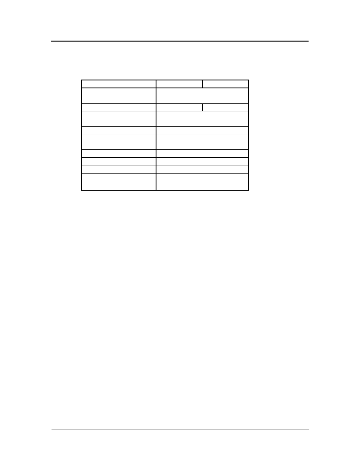
Series Comparison Table
Model FB2410 FB2410A
Processor
VGA Chipset
CRT / LCD CRT/TFT/LVDS
Watchdog Timer Yes
Multi I/O 2S/1P/FDD/IDE
Serial Port One RS232,One RS-232/RS485
Parallel Yes
FDD Yes
Enhanced IDE One
Compact Flash Socket
USB 1.1 Two
RJ45 port (10/100Mbps) One
Dimensions (Unit: mm) 90.2(D) x 95.9(W)
STPC ATLAS
CRT
One
2
Page 8
FabiaTech Corporation
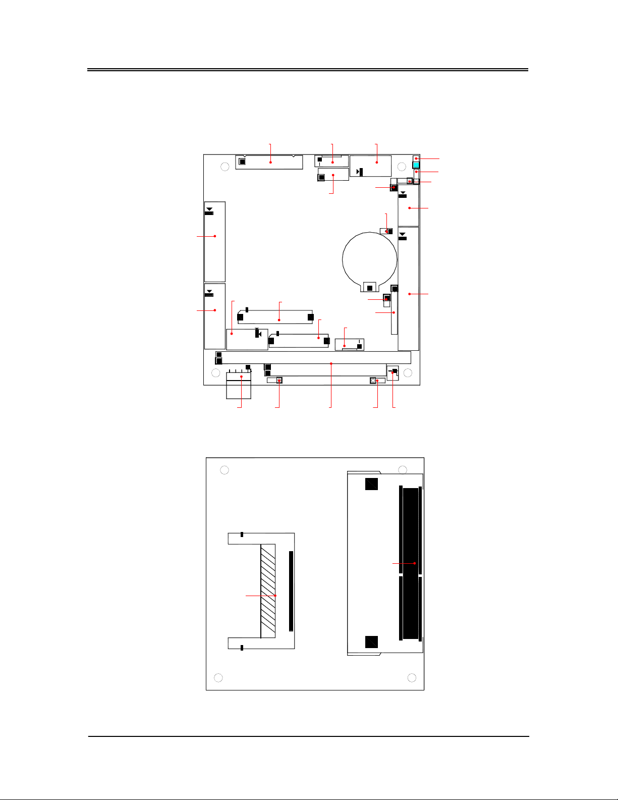
Layout
CN4
J1 CN1 CN2
J2
J4
LED1
BT1
J3
JP1
JP4
CN3
CN6
CN9
J5
J6
CN10
CN8
CN7
J7 JP2 JP3BUS1 J8
DIMM1
CN5
CF1
3
Page 9

FabiaTech Corporation
Specifications
STPC ATLAS CPU and 8KB L1 cache inside the CPUs.
Supporting One So-DIMM socket for up 128MB SDRAM
One 10M/100M Base-TX Ethernet port.
Supports CRT port and TFT/LVDS LCD with up to 4MB shared memory.
One RS-232, one RS-232/RS-485 ports, parallel, floppy, and PCI IDE interface.
Compact Flash socket for 3.3V Compact Flash and Micro Drives.
PS/2 compatible keyboard and mouse interface.
Providing header for external speaker and hard disk access LED.
Two USB (1.1) ports and Software programmable watchdog timer.
Flash BIOS with easy upgrade utility.
PC/104 form factor, 90.2 mm x 95.9 mm (3.55” x 3.775”)
Power requirement: +5V only, 1.5A maximum.
4
Page 10

FabiaTech Corporation
Packing List
Upon receiving the package, verify the following things. If any of the mentioned
happens, contact us for immediate service.
• Unpack and inspect the FB2410 package for possible damage that may
occur during the delivery process.
• Verify the accessories in the package according to the packing list and see
if there is anything missing or incorrect package is included.
• If the cable(s) you use to install the FB2410 is not supplied from us, please
make sure the specification of the cable(s) is compatible with the FB2410
system.
Note: After FB2410 is installed, it is recommended that you keep the diskette or
CD that contains drivers and document files, and keep the document
copies, or unused cables in the carton for f uture use.
The following list the accessories that may be included in your FB2410 package.
Some of the accessories are optional shipped only upon order.
• One FB2410 All-In-One PC/104 CPU board.
• One VGA (CRT interface) adapter cable.
• One 44-pin hard disk drive interface cable.
• One 20-pin to 34-pin floppy driver interface cable.
• Two serial port adapter cables.
• One PS2 keyboard and mouse port adapter cable.
• One 10-pin LAN adapter cable with FB4605A board.
• One USB adapter cable. (Optional items)
• One compact disc containing manual file in PDF format and necessary
drivers and utilities.
5
Page 11

FabiaTech Corporation
6
Page 12

FabiaTech Corporation
Chapter 2 Hardware Installation
This chapter introduces the system connectors & jumper settings, and guides you to
apply them for field application.
Before Installation
Before you install the system, make sure you follow the below descriptions.
1. Before re moving the board from its anti-static bag, wear an anti-static strap to
prevent the generation of Electricity Static Discharge (ESD). The ESD may be
generated by man’s physical touch. It may do damage to the board circuit.
2. Install any connector, module, or add on card, be sure that the power is
disconnected from the system board. If not, this may damage the system
board components, module, or the add-on-card.
3. When you connect the connectors and memory modules, be careful with the
pin orientations.
7
Page 13

FabiaTech Corporation
Hardware Features
The following list is for the setup of the connectors and jumpers of the FB2410.
Item Description
CN1 6-pin for Keyboard and Mouse connector (JST)
CN2 10-pin 2.0mm COM2 RS-232/RS485 port connector (IDC)
CN3 10-pin 2.0mm COM1 RS-232 port connector (IDC)
CN4 26-pin 2.0mm parallel port connector (IDC)
CN5 44-pin 2.0mm IDE hard disk connector (IDC)
CN6 20-pin 2.0mm floppy connector (IDC).
CN7 40-pin LCD Connector with 24 bit LCD signals (DF13)
CN8 10-pin 2.0mm CRT connector (IDC)
CN9 30-pin LCD Connector with LVDS LCD signals (DF13)
CN10 5-pin Power Connector for LCD inverter board (JST)
CF1,JP1 Compact Flash Socket and Master/Slave Select
JP2 RS232/RS-485 Select Header
JP3 Clear CMOS data and Select external battery header
JP4 Terminator header for RS485
J1 10-pin for RJ45-Lan 2.54mm connector (JST)
J2 10-pin USB ports #0/1 2.54mm connector header
J3 2-pin Reset header
J4 2-pin for HDD LED indicator header
J5 2-pin for external speaker header
J6 Reserved
J7 4-pin Power connector
J8 2-pin for external battery header
LED1 Power and watchdog of LED indicator
BUS1 PC-104 Connector
DIMM1 SDRAM So-DIMM Socket 144-pin
8
Page 14
FabiaTech Corporation
y
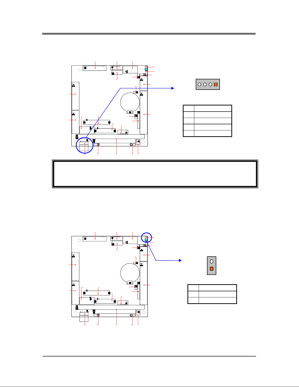
J7: Power Connector (4-pin 2.5mm JST)
J1 CN1 CN2
CN9
J4
LED1
BT1
J5
J6
CN10
CN4
CN6
CN8
J2
CN7
J3
JP1
JP4
CN3
CN5
4
PIN
1
2
3
4
1
Signal
VCC (+5V)
Ground
Ground
VDD (+12V)
Note: FB2410 needs +5V only,
J7 JP2 JP3BUS1 J8
+12V is not necessar
.
Note: Be careful with the pin orientation when installing power connector. A wrong
connection can easily destroy your FB2410 board.
J3: Reset Header
J3 is a 2-pin header for connecting to system reset button. Shorting the circuit of
the 2 pins makes the hardware reset and FB2410 restart system. It is similar to power
off the system and then power it on again.
J1 CN1 CN2
J3
JP1
JP4
CN3
CN5
PIN
1
2
J3
2
1
Signal
Reset +
Reset -
CN4
CN6
CN8
CN7
J2
CN9
J4
LED1
BT1
J5
J6
CN10
J7 JP2 JP3BUS1 J8
9
Page 15
FabiaTech Corporation
J1
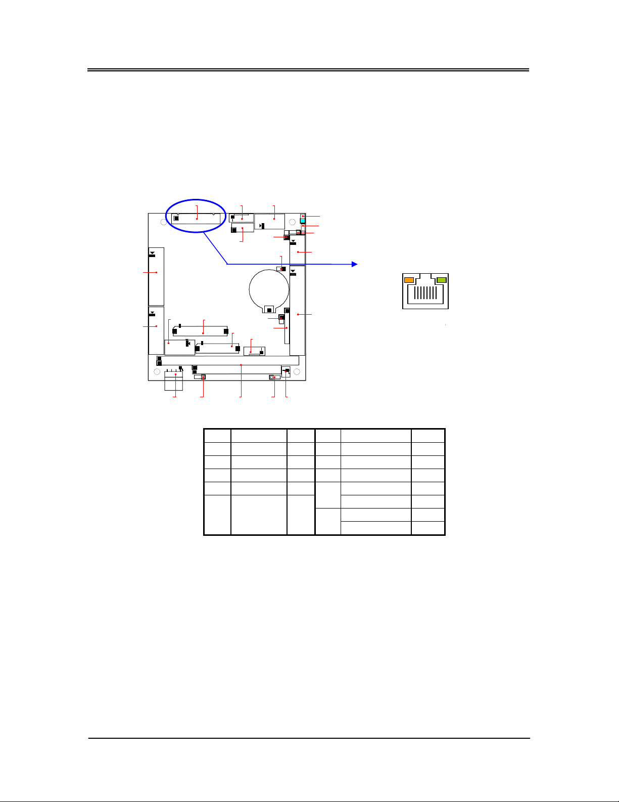
J1: RJ45 LAN /Adapter Connector with LED indicators
FB4605A is a RJ45 connector with 2 LEDs for LAN. The left side LED (orange)
indicates data which is being accessed and the right side LED (green) indicates online status. (On indicates on-line and Off indicates off-line) J1 provides twist-pair
signals of LAN port if you got LAN version and adapter board (FB4605A) with cable.
The following lists the pin assignments of J1 to RJ45 connector on the FB4605A LAN
adapter board:
J1 CN1 CN2
J3
JP1
JP4
RJ45 connector on FB4605A adapter
CN3
board
CN4
J2
J4
LED1
BT1
CN6
CN9
J5
J6
CN10
CN8
J7 JP2 JP3BUS1 J8
CN7
The following list the pin assignments of J1.
J1 Signal RJ45
1 TPTX+ 1 6 Access LED
2 TPTX - 2 7 On-Line LED
3 TPRX+ 3 8 Case GND
4 TPRX - 6 FBG1 4 9
5 LED
Common
CN5
1
(Fron t V iew)
8
Signal RJ45
-
-
-
-
FBG1 5
FBG2 7
10
FBG2 8
10
Page 16
FabiaTech Corporation
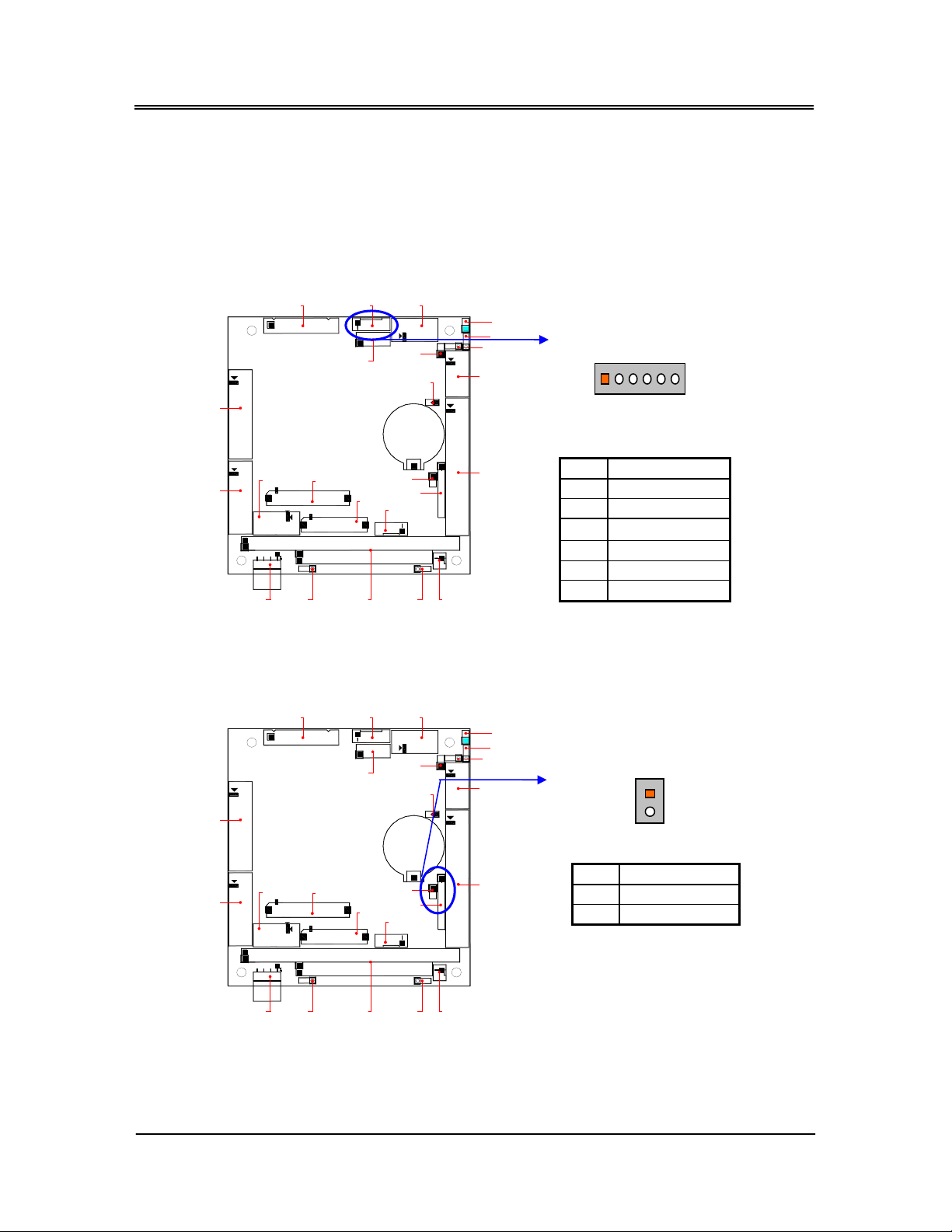
CN1: Keyboard/Mouse Connector
CN1 is a 6-pin 2.0mm JST connector, use the included KB/MS adapter cables you
can attach standard PS/2 type keyboard and mouse.
J1 CN1 CN2
J3
CN4
J2
J4
LED1
BT1
JP1
JP4
CN3
CN1
1 6
CN6
CN8
CN7
CN9
J5
J6
CN10
J7 JP2 JP3BUS1 J8
J5: External Speaker Header
J1 CN1 CN2
CN9
J4
LED1
BT1
J5
J6
CN10
CN4
CN6
CN8
J2
CN7
CN5
J3
JP1
JP4
CN3
CN5
PIN
1 Mouse Data
2 Keyboard Data
3 Ground
4 VCC
5 Mouse Clock
6 Keyboard Clock
Signal
J5
1
2
PIN
1 Speaker+
2 Speaker-
Signal
J7 JP2 JP3BUS1 J8
11
Page 17
FabiaTech Corporation
1
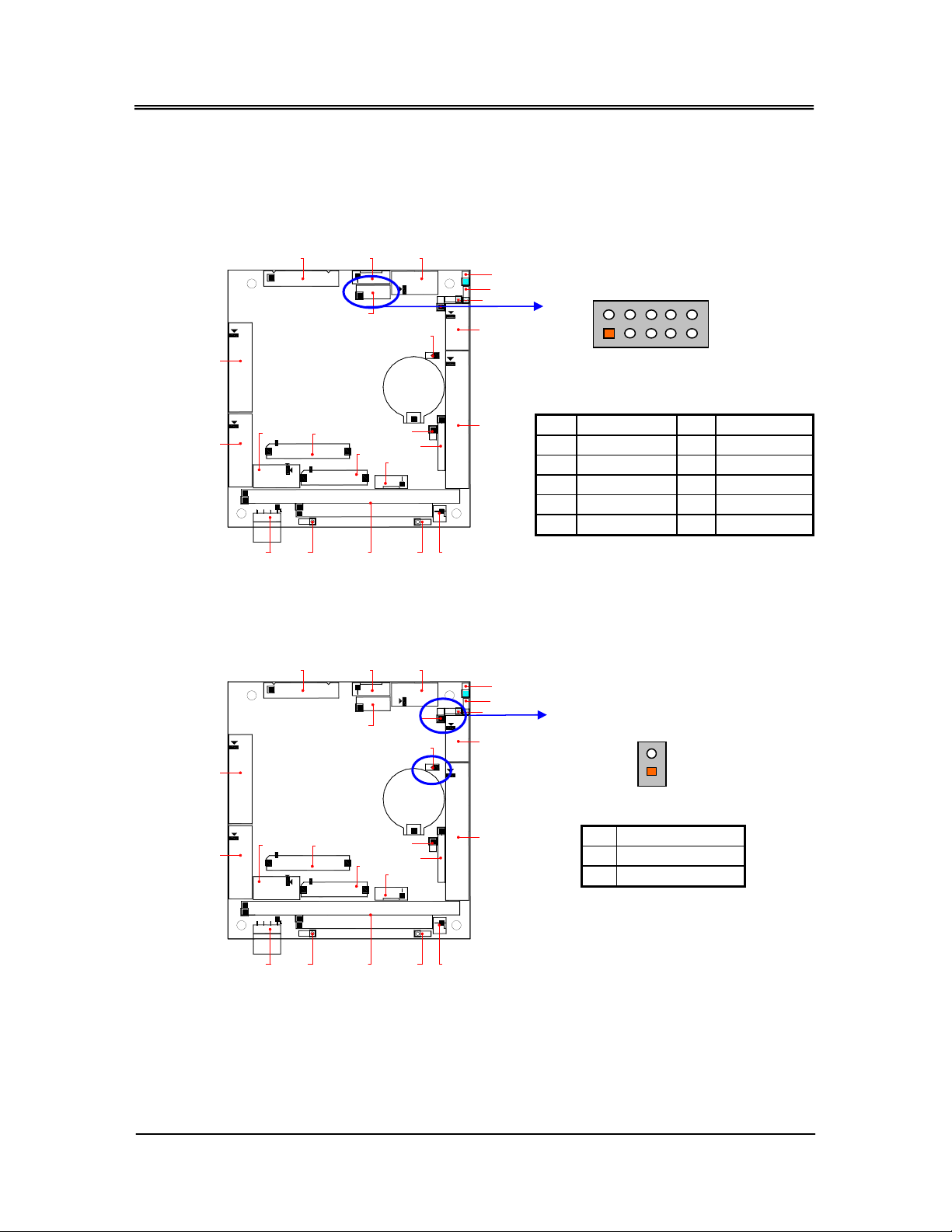
J2: USB Connector
Use the USB adapter cable and FB4641 board, you can attach up to 2 US B devices.
J1 CN1 CN2
J2
2
1
10
9
CN4
J2
J4
LED1
J3
JP1
JP4
CN3
BT1
PIN Description PIN Description
1 USBV0 2 Case Ground
3 USBD0- 4 USBG1
5 USBD0+ 6 USBD1+
7 USBG0 8 USBD19 Case Ground 10 USBV1
CN6
CN9
J5
J6
CN10
CN8
CN7
J7 JP2 JP3BUS1 J8
CN5
LED1: Power/WatchDog LED indicator, J4: External HDD LED Header
J1 CN1 CN2
J3
JP1
JP4
J4
CN3
2
CN4
J2
J4
LED1
BT1
CN6
CN9
J5
J6
CN10
CN8
CN7
J7 JP2 JP3BUS1 J8
CN5
PIN
1
2
Signal
HDD LED+
HDD LED -
12
Page 18
FabiaTech Corporation
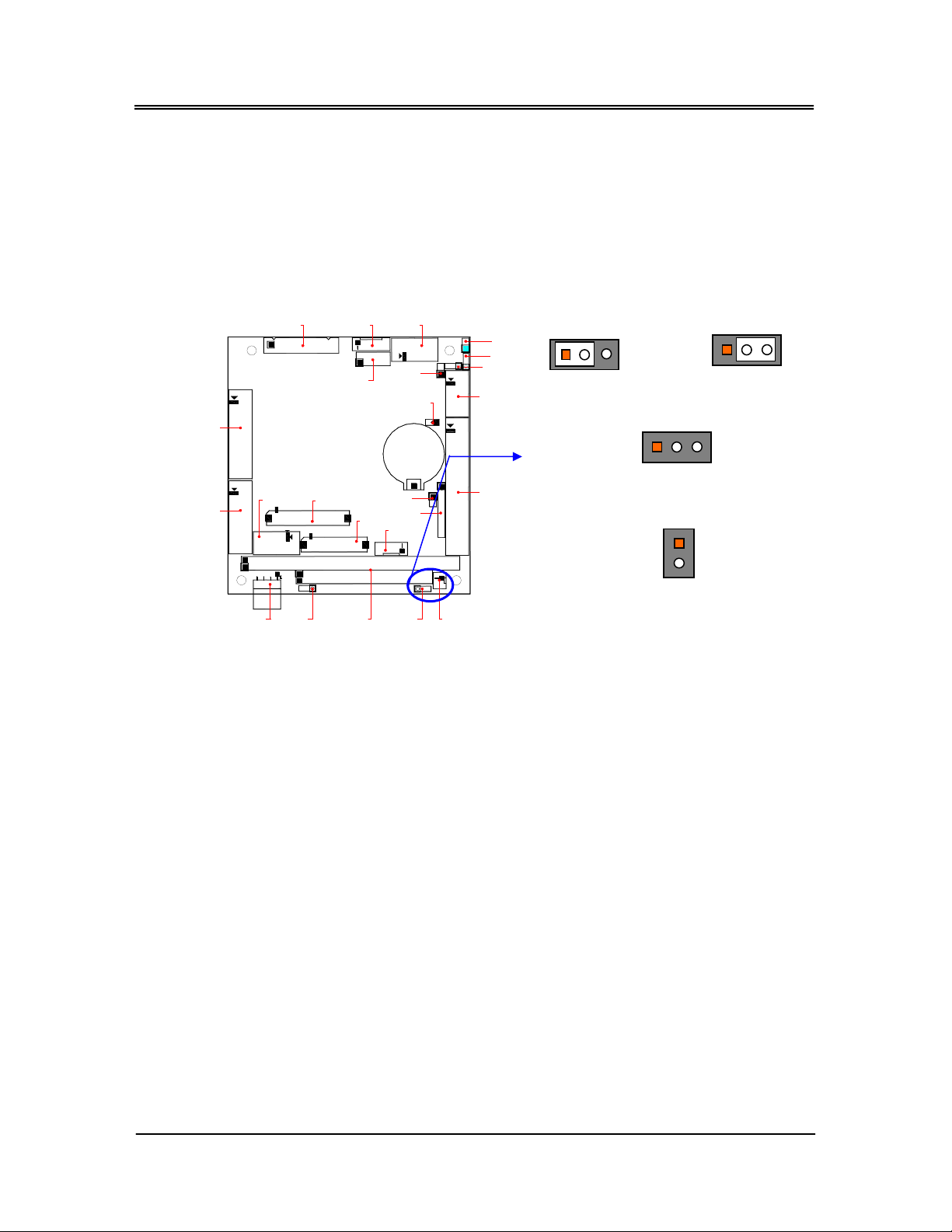
J8 & JP3: External Battery Connector and Battery Select Jumper
J8 is used to connect an external battery pack if on-board Lithium battery is empty,
and please setting JP3 properly of in-board battery or external battery .You can
use JP3 to clear CMOS data. The CMOS store information like system date, time,
boot up device, password, IRQ… which are se t up with the BIOS. To clear the
CMOS, set JP3 to open and then return to 1-2 before system power off. The default
setting is 1-2.
JP3
CN4
J1 CN1 CN2
J2
J4
LED1
BT1
J3
JP1
JP4
CN3
On-Board Battery
12
Default
3
External Battery
12 3
12 3
CN6
CN9
J5
CN10
CN8
J7 JP2 JP3
CN7
BUS1 J8
J6
CN5
Clear CMOS Data
J8
1
2
Pin 1:Battery +
Pin 2:Battery Note: 2.6V ~3.6V
13
Page 19
FabiaTech Corporation
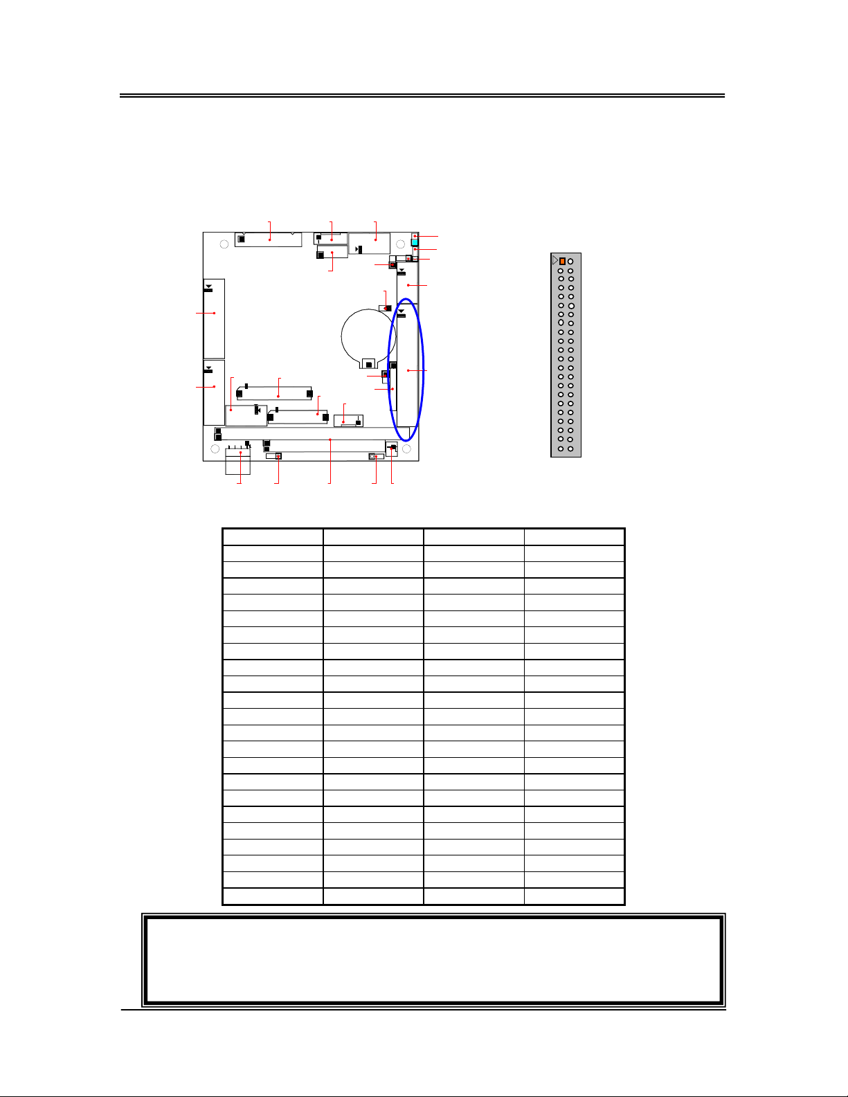
CN5: IDE hard Disk Connectors
CN5 is 44-pin 2.0mm IDC connec tors. Use the included hard disk cables to attach
up to two 2.5” hard disk drives.
CN4
CN6
J1 CN1 CN2
CN9
J4
LED1
BT1
J5
J6
CN10
J2
CN8
J7 JP2 JP3BUS1 J8
CN7
The following table lists the pin description of CN5.
Pin Description Pin Description
1 -RESET 2 GROUND
3 DATA 7 4 DATA 8
5 DATA 6 6 DATA 9
7 DATA 5 8 DATA 10
9 DATA 4 10 DATA 11
11 DATA 3 12 DATA 12
13 DATA 2 14 DATA 13
15 DATA 1 16 DATA 14
17 DATA 0 18 DATA 15
19 GROUND 20 NOT USED
21 IDEDREQ 22 GROUND
23 -IOW A 24 GROUND
25 -IOR A 26 GROUND
27 IDEIORDYA 28 GROUND
29 -DACKA 30 GROUND
31 AINT 32 GROUND
33 SA 1 34 Not Used
35 SA 0 36 SA 2
37 CS 0 38 CS 1
39 HD LED A 40 GROUND
41 VCC 42 VCC
43 GROUND 44 Not Used
J3
JP1
JP4
CN3
CN5
CN5 – Hard disk connector
1
43
2
44
Note: Be careful with the pin orientation wh en installing connectors and the cables.
A wrong connection can easily destroy your hard disk. CN5 is used to connect a
2.5" HDD with included 44-pin flat-cable or 44-pin DiskOnModule directly
.
14
Page 20
FabiaTech Corporation
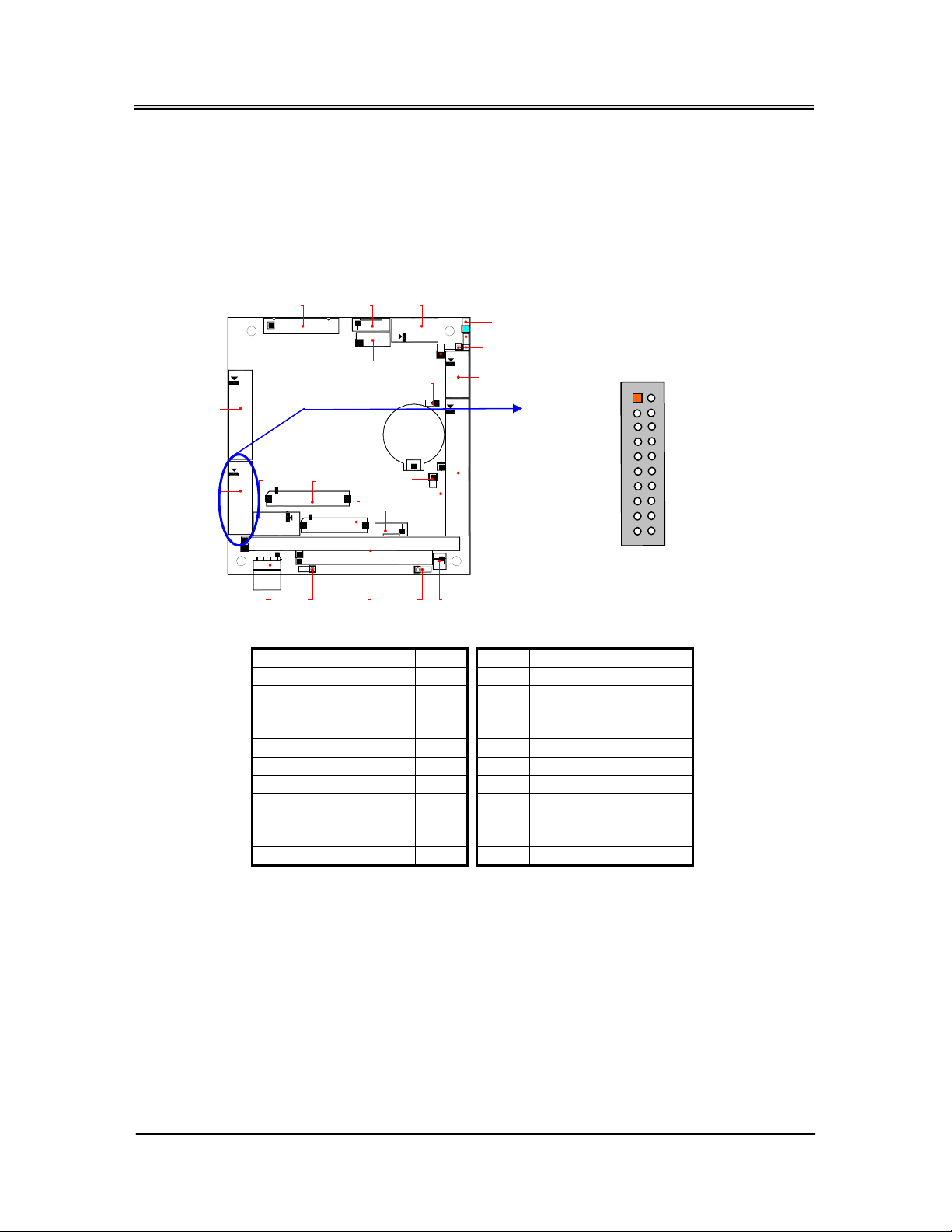
CN6: Floppy Connector
The included floppy drive interface cable is used to transfer 20-pin connector into
standard 34-pin connector. The following table shows signal connections between
20-pin & 34-pin connectors.
J1 CN1 CN2
J3
JP1
JP4
CN3
CN6
1
2
CN4
J2
J4
LED1
BT1
CN6
CN5
19
20
CN9
J5
J6
CN10
CN8
J7 JP2 JP3BUS1 J8
CN7
The following table shows signal connections.
20-pin Signal 34-pin
1 Drive Enable A 2
2 -Index 8 13 -Write Enable 24
3 -Select A 12 14 -Track 0 26
4 Ground 11 15 -Write Protect 28
5 -Motor A 16 16 Ground 29
6 - Select B 14
7 -Motor B 10 18 -Head 32
8 Ground 9 19 -Disk Change 34
9 -Direction 18 20 Ground 31
10 -Step 20
11 -Write Data 22 - No Connection Others
20-pin
12 Ground 23
17 -Read Data 30
Signal 34-pin
15
Page 21
FabiaTech Corporation
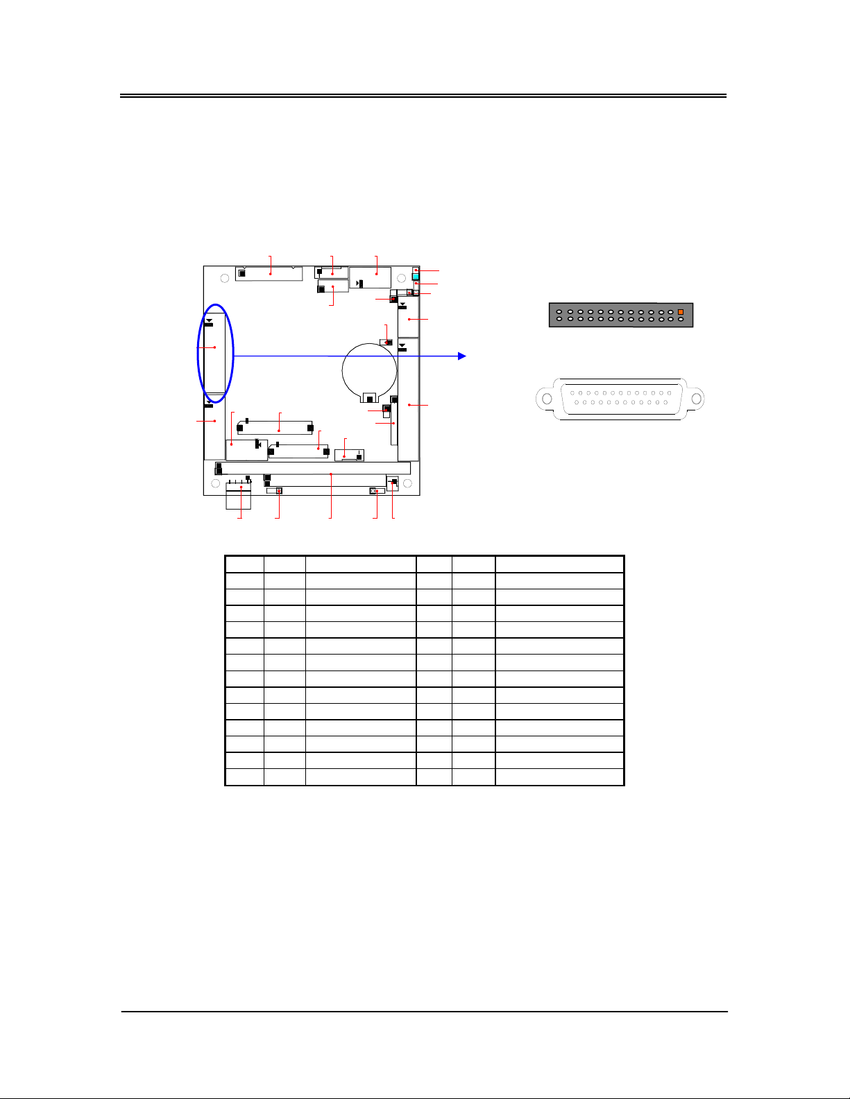
CN4: 26-pin Parallel Port Connector
The included printer interface cable is used to transfer 26-pin connector into
standard DB25 connector.
CN4
CN6
J1 CN1 CN2
J3
JP1
JP4
CN3
CN5
-- No Used
CN9
J4
LED1
BT1
J5
J6
CN10
J2
CN8
J7 JP2 JP3BUS1 J8
CN4 DB-25 Signal CN4 DB-25
1 1 -STROBE 2 14 -AU TO F O R M F E E D
3 2 DATA 0 4 15 -ERROR
5 3 DATA 1 6 16 -INITIALIZE
7 4 DATA 2 8 17 -PRINTER SELECT IN
9 5 DATA 3 10 18 Ground
11 6 DATA 4 12 19 Ground
13 7 DATA 5 14 20 Ground
15 8 DATA 6 16 21 Ground
17 9 DATA 7 18 22 Ground
19 10 -ACKNOWLEDGE 20 23 Ground
21 11 BUSY 22 24 Ground
23 12 PAPER 24 25 Ground
25 13 PRINTER SELECT 26
CN7
25
26
Signal
CN4
1
2
16
Page 22
FabiaTech Corporation
2 1 9 10
9 10 2
2
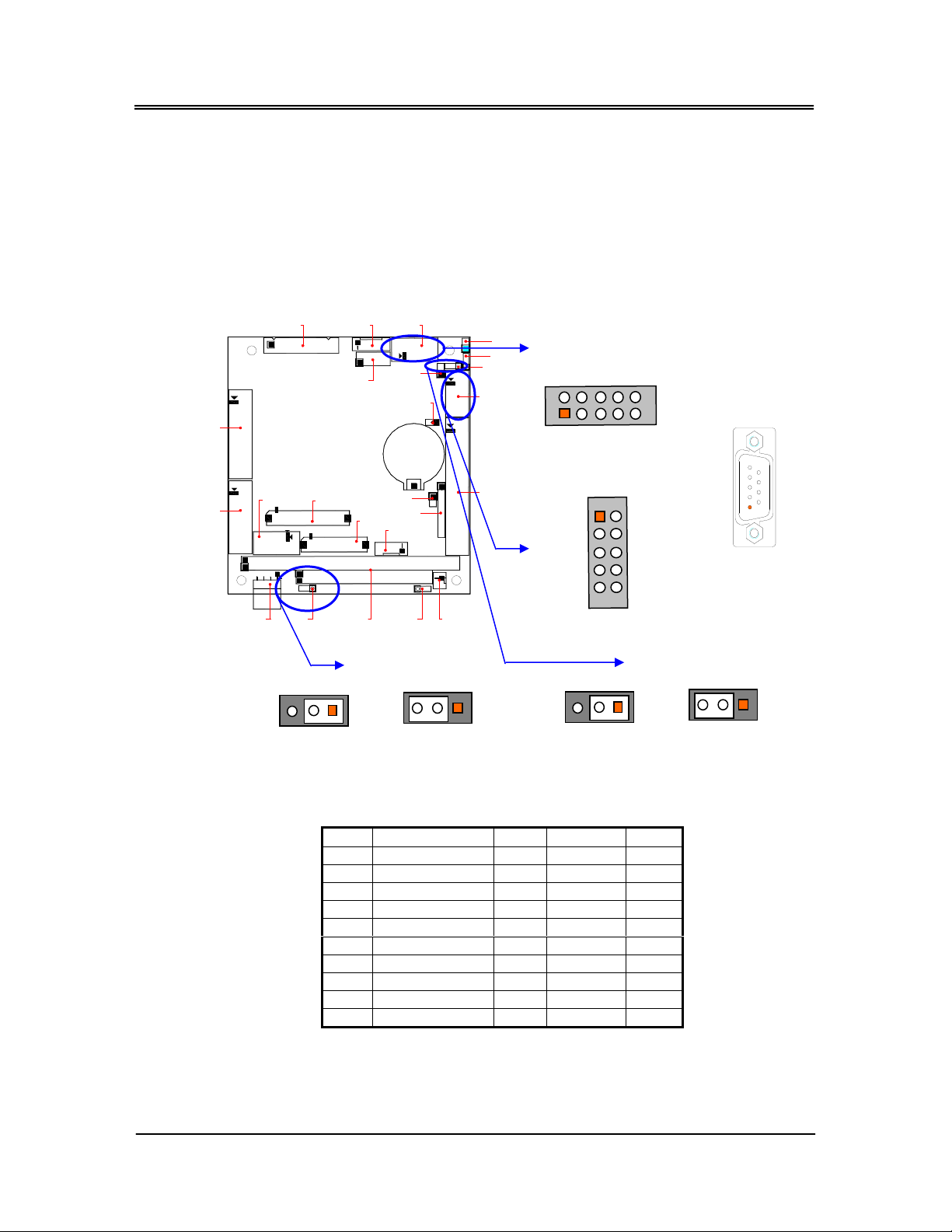
CN2 & CN3: Serial Port Connectors RS-232C Pin Definitions
CN3 (COM1) & CN2 (COM2) are 10-pin 2.0mm IDC connectors. The included
serial port adapter cables are used to transfer 10-pin 2.0mm IDC into standard DB9 connector. The serial port 2 is designed for multiple proposes. Use JP2 selects the
RS-232 or RS-485, and JP4 provides terminator select of RS-485 mode. The
following tables show the signal connections of these connectors and the
included adapter cable for CN2 & CN3:
J1 CN1 CN2
J3
JP1
JP4
CN3
CN4
J2
J4
LED1
BT1
CN2
CN3
5
DB9
9
CN6
CN8
J7 JP2 JP3BUS1 J8
CN7
CN9
JP2
3
2
1
RS-232
Factory Preset
CN3 Signal CN2
1 -DCD2 1 1
2 -DSR2 2 6
3 RXD2 3 485- 2
4 -RTS2 4 7
5 TXD2 5 485+ 3
6 -CTS2 6 8
7 -DTR2 7 4
8 -RI2 8 9
9 GROUND 9 5
10 CASE GROUND 10 Shield
J5
J6
CN10
3
RS-485
CN5
1
1
6
JP4
2
3
32
1
Pin 1,2 Close:
1
Terminator
Enabled
Pin 2,3 Close:
Terminator
Disable
Default
1
RS485 DB9
17
Page 23
FabiaTech Corporation
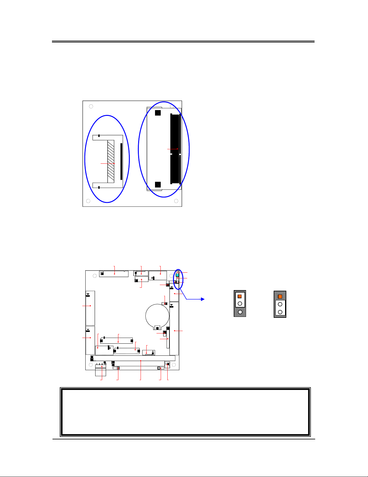
DIMM1: So-DIMM Socket
The DIMM1 socket on the solder side accepts 64MB to 128MB of SDRAM modules
DIMM1
CF1
CF1 & JP1: Compact Flash Socket and Master/Slave Select
The Compact Flash socket CF1 (on the solder side) is supports 3.3V Compact Flash
and Micro Drives. JP1 is used to select ma ster/slave device of this socket. Be sure to
ward off the same master/slave setting with which connects to IDE (CN5)
connector, if you use CF1 and CN5 simultaneously.
J1 CN1 CN2
J3
JP1
CN4
CN6
CN9
J4
LED1
BT1
J5
J6
CN10
J2
CN8
J7 JP2 JP3BUS1 J8
CN7
JP4
CN3
CN5
Master
JP1
1
2
3
1
2
3
Slave
Default
Note: The Compact Flash socket supports 3.3V Compact Flash and Micro Drives.
The JP1 is used to select master/slave device of this socket and the default is
slave (close). Be sure not to set master/slave to the same IDE connector, if you
use CF and IDE hard disk simultaneous ly.
18
Page 24
FabiaTech Corporation
BUS1: PC/104 Bus Connectors
CN4
CN6
J1 CN1 CN2
CN9
J4
LED1
BT1
J5
J6
CN10
J2
CN8
J7 JP2 JP3BUS1 J8
CN7
J3
JP1
JP4
CN3
CN5
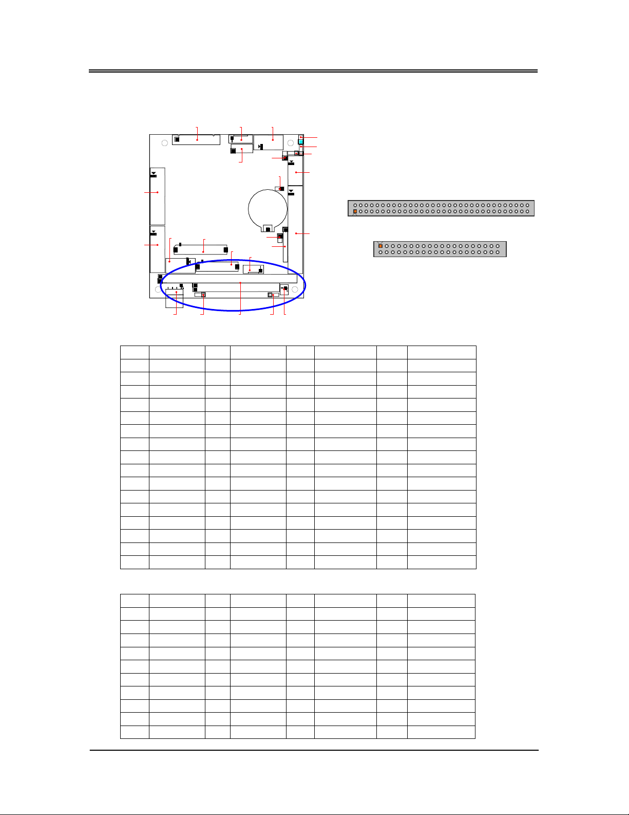
BUS1 – BUS A & B
BUS1 – BUS C & D
PC/104 A & B Pin
Pin
Signal
Pin Signal Pin
Signal Pin
A1 -IOCHK A17 SA14 B1 Ground B17
A2 SD7 A18 SA13 B2 RSTDRV B18
A3 SD6 A19 SA12 B3
A4 SD5 A20 SA11 B4
A5 SD4 A21 SA10 B5
A6 SD3 A22 SA9 B6
A7 SD2 A23 SA8 B7
A8 SD1 A24 SA7 B8
A9 SD0 A25 SA6 B9
A10 IORDY A26 SA5 B10
+5V B19 -REFRESH
IRQ9 B20
-5V B21
DRQ2 B22
-12V) B23
-ZWS B24
+12V B25
Key1 B26
A11 AEN A27 SA4 B11 -MEMW B27
A12 SA19 A28 SA3 B12 -MEMR B28
A13 SA18 A29 SA2 B13
A14 SA17 A30 SA1 B14
-IOW B29
-IOR B30
A15 SA16 A31 SA0 B15 -DACK3 B31
A16 SA15 A32 Ground B16
DRQ3 B32
Signal
-DACK1
DRQ1
BUSCLK
IRQ7
IRQ6
IRQ5
IRQ4
IRQ3
-DACK2
TC
ALE
+5V
OSC
Ground
Ground
PC/104 C& D Pin
Pin
Signal
Pin Signal Pin
Signal Pin
Signal
C1 GND C11 MEMW# D1 Ground D11 -DACK#5
C2 SBHE C12 SD8 D2 MEMCS16# D12
DREQ5
C3 LA23 C13 SD9 D3 IOCS16# D13 DACK#6
C4 LA22 C24 SD10 D4
C5 LA21 C25 SD11 D5
C6 LA20 C26 SD12 D6
C7 LA19 C27 SD13 D7
C8 LA18 C28 SD14 D8
C9 LA17 C29 SD15 D9 DACK#0 D19
C10 MEMR# C20 KEY D10 DREQ0 D20
IRQ10 D14
DREQ6
IRQ11 D15 DACK#7
IRQ12 D16
IRQ15 D17
DREQ7
VCC
IRQ14 D18 -MEMCS16-
GND
GND
19
Page 25

FabiaTech Corporation
20
Page 26
FabiaTech Corporation
Chapter 3 Installing CRT & LCD Display
This chapter describes the configuration and installation procedure of LCD and CRT
displays. Both CRT and LCD displays may be used at the same time. However, each
type of LCD requires different BIOS. This section describes the configuration and
installation procedure using LCD display. Skip this section if you are using CRT monitor
only.
• LCD Flat Panel Display
• CRT & LCD Display
LCD FLAT PANEL DISPLAY
Using the BIOS setting for different types of LCD pane, then set your system properly
and configures BIOS setting for the right type of LCD panel you are using.
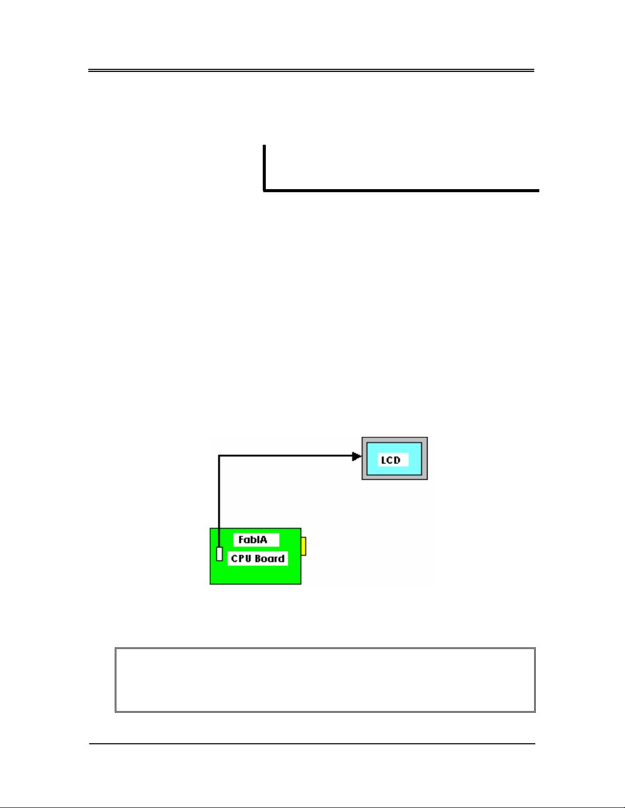
The following shows the block diagram of using FB2410 for LCD display.
LCD Panel Block Diagram
The diagram shows that FB2410 needs components to be linked with a LCD panel.
NOTE: Be careful with the pin orienta tion whe n installing connectors and the cables.
A wrong connection can easily destroy your LCD panel. The pin 1 of the
cable connectors is indicated with a sticker and the pin1 of the ribbon
cable usually has a different color.
21
Page 27
FabiaTech Corporation
15
CRT Display (CN8)
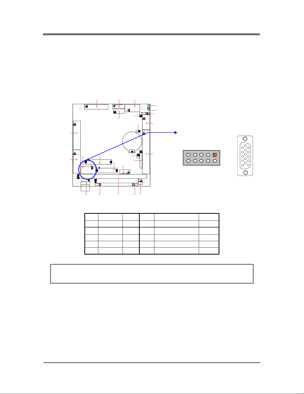
The FB2410x supports a CRT colored monitor. It can be connected to create a
compact video solution for the industrial environment. 4MB simulated VRAM allows
a maximum CRT resolution of 1280X1024 with 24 bpp at 75Hz. The following table
and figure illustrate the pin definition of CN8 and D-sub 15-pin on the CRT adapter
cable:
J1 CN1 CN2
J3
JP1
JP4
CN3
CN5
9
10
CN8
1
2
CN4
CN6
CN8
CN7
J2
CN9
J4
LED1
BT1
J5
J6
CN10
1
5
DB15
6
11
J7 JP2 JP3BUS1 J8
Pin Signal DB-15
Pin
Signal DB15
1 RED 1 2 Case Ground Case
3 GREEN 2 4 Digital Ground 5,10
5 BLUE 3 6 Analog Ground 6,7,8
7 VSYNC 14 8 DDC Data 12
9 HSYNC 13 10 DDC Clock 15
NOTE: Be careful with the pin orientation when installing VGA connector and the
cable.
10
22
Page 28
FabiaTech Corporation
40 39
29
CN10
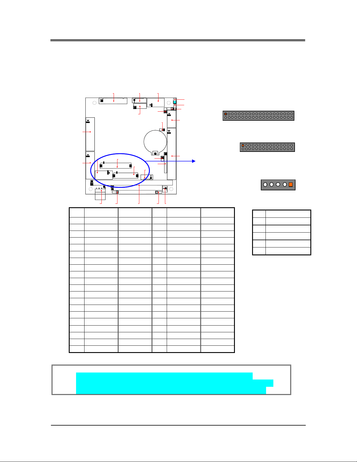
CN7, CN9 & CN10: LCD Connector and Power connector
CN7 supports 18-bit TTL LCD signals, CN9 supports 18-bit LVDS LCD signals, and
CN10 is the power connector for inverter board.
J1 CN1 CN2
J3
CN4
J2
J4
LED1
BT1
JP1
JP4
CN3
1
2
1
CN7
CN9
CN5
CN7 CN9
+5V
NC Ground
NC -
NC Ground
FP1(R1) +3.3V
FP3(R3) +5V
FP5(R5)
Ground
FP (VS)
LP (HS)
TX0+
-
CN6
CN8
CN7
CN9
J5
J6
CN10
J7 JP2 JP3BUS1 J8
Pin CN7 CN9 Pin
1
3 Ground TX0- 4 Ground Ground
5 +3.3V TX1+ 6 +3.3V TX17 NC Ground 8 Ground TX2+
9 NC TX2- 10
11 FP12(B0) TXCLK+ 12 FP13(B1) TXCLK-
13 FP14(B2) Ground 14 FP15(B3) -
15 FP16(B4) - 16 FP17(B5) Ground
17 NC - 18
19 FP6(G0) Ground 20 FP7(G1) -
21 FP8(G2) - 22 FP9(G3) Ground
23 FP10(G4) - 24 FP11(G5)
25 NC Ground 26
27 FP0(R0) +3.3V 28
29 FP2(R2) +5V 30
31 FP4(R4) 32
33 Ground 34
35 SHFCLK 36
37 DE 38
39 ENVDD 40 ENAVEE
+5V
Ground 2
2
5
Pin CN10
1 +12 V
2 GND
3 ENABLK
4 N.C
5 +5 V
30
1
NOTE: 1. Different LCD panels use different BIOS and pin connections.
2. If any trouble occurs when connecting FB2410 with LCD panels, you
could contact technical support division of FabiaTech Corporation.
23
Page 29

FabiaTech Corporation
24
Page 30

FabiaTech Corporation
Chapter 4 BIOS Setup
This chapter describes the BIOS setup.
Overview
BIOS are a program located on a Flash memory chip on a circuit board. It is used
to initialize and set up the I/O peripherals and interface cards of the system, which
includes time, date, hard disk drive, the PCI bus and connected devices such as
the video display, diskette drive, and the keyboard. This program will not be lost
when you turn off the system.
The BIOS provides a menu-driven interface to the console subsystem. The console
subsystem contains special software, called firmware that interacts directly with the
hardware components and facilitates interaction between the system hardware
and the operating system.
The BIOS default values ensure that the system will function at its normal capability.
In the worst situation, the user may ha ve corrupted the original settings set by the
manufacturer.
All the changes you make will be saved in the system RAM and will not be lost after
power-off.
When you start the system, the BIOS will perform a self-diagnostics test called Power
on Self Test (POST) for all the attached devices, accessories, and the system. Press
the [Del] key to enter the BIOS Setup program, and then the main menu will show
on the screen.
Note: Change the parameters when you fully understand their functions and
subsequence.
25
Page 31
FabiaTech Corporation
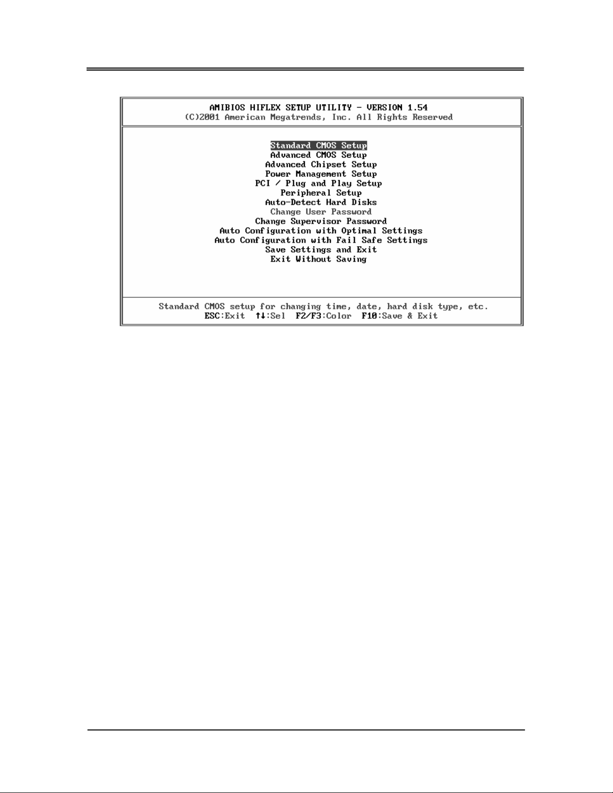
BIOS Functions
On the menu, you can perform the fo llowing functions
1. Standard CMOS Setup
2. Advanced CMOS Setup
3. Advanced Chipset Setup
4. Power Management Setup
5. PCI/ Plug and Play Setup
6. Peripheral Setup
7. Auto-Detect Hard Disks
8. Change User Password
9. Change Supervisor Password
10. Auto Configuration with Optimal Settings: to auto configure the system
according to optimal setting with pre-defined values. This is also the factory
default setting of the system when you receive the board.
11. Auto Configuration with Fail Safe Settings: to configure the system in fail-safe
mode with predefined values.
12. Save Settings and Exit: perform this function when you change the setting and
exit the BIOS Setup program.
13. Exit without saving: perform this function when you want to exit the program
and do not save the change.
26
Page 32

FabiaTech Corporation
Keyboard Convention
On the BIOS, the following keys can be used to operate and manage the menu:
Item Function
ESC To exit the current menu or message
Page Up/Page Down To select a parameter
F1 To display the help menu if you do not know the
purpose or function of the item you are going to
configure
F2/F3 To change the color of the menu display. F2 is to go
forward and F3 is to go backward.
UP/Down Arrow Keys To go upward or downward to the desired item
27
Page 33
FabiaTech Corporation
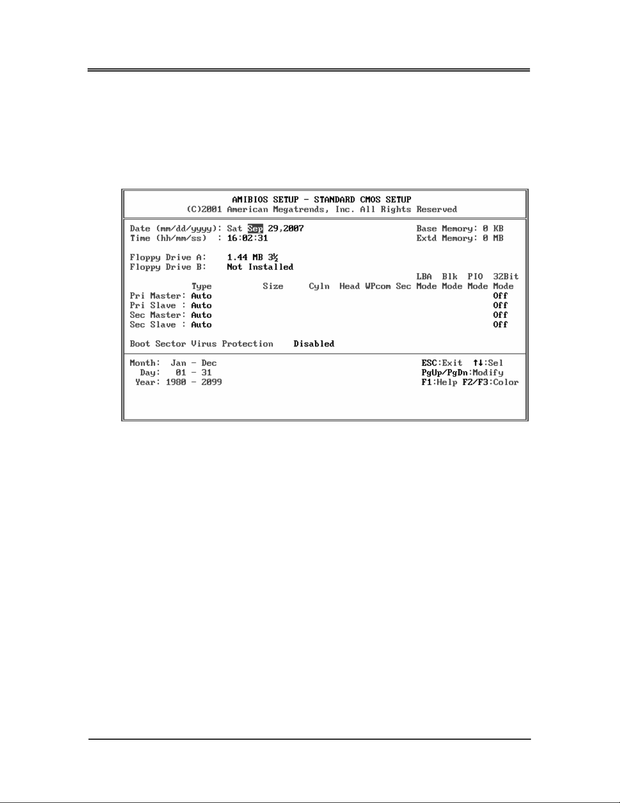
STANDARD CMOS SETUP
This section describes basic system hardware configuration, system clock setup
and error handling. If the CPU board is already installed in a working system, you
will not need to select this option anymore.
Date & Time Setup
Highlight the <Date> field and then press the [Page Up] /[Page Down] or [+]/[-]
keys to set the current date. Follow the month, day and year format.
Highlight the <Time> field and then press the [Page Up] /[Page Down] or [+]/[-]
keys to set the current date. Follow the hour, minute and second format.
The user can bypass the date and time prompts by creating an AUTOEXEC.BAT file.
For information on how to create this file, please refer to the MS-DOS manual.
Floppy Setup
The <Standard CMOS Setup> option records the types of floppy disk drives installed
in the system.
To enter the configuration value for a particular drive, highlight its corresponding
field and then select the drive type using the left-or right-arrow key.
Hard Disk Setup
The BIOS supports various types for user settings, The BIOS supports <Pri Master>, <Pri
Slave>, <Sec Master> and <Sec Slave> so the user can install up to four hard disks.
28
Page 34

FabiaTech Corporation
For the master and slave jumpers, please refer to the hard disk’s installation
descriptions and the hard disk jumper settings.
You can select <AUTO> under the <TYPE> and <MODE> fields. This will enable auto
detection of your IDE drives during boot up. This will allow you to change your hard
drives (with the power off) and then power on without having to reconfigure your
hard drive type. If you use older hard disk drives, which do not support this feature,
then you must configure the hard disk dr ive in the standard method as described
above by the <USER> option.
Boot Sector Virus Protection
This option protects the boot sector and partition table of your hard disk against
accidental modifications. Any attempt to write to them will cause the system to
halt and display a warning message. If this occurs, you can either allow the
operation to continue or use a bootable virus-free floppy disk to reboot and
investigate your system. The default setting is <Disabled>. This setting is
recommended because it conflicts with new operating systems. Installation of new
operating system requires that you disable this to prevent write errors.
29
Page 35
FabiaTech Corporation
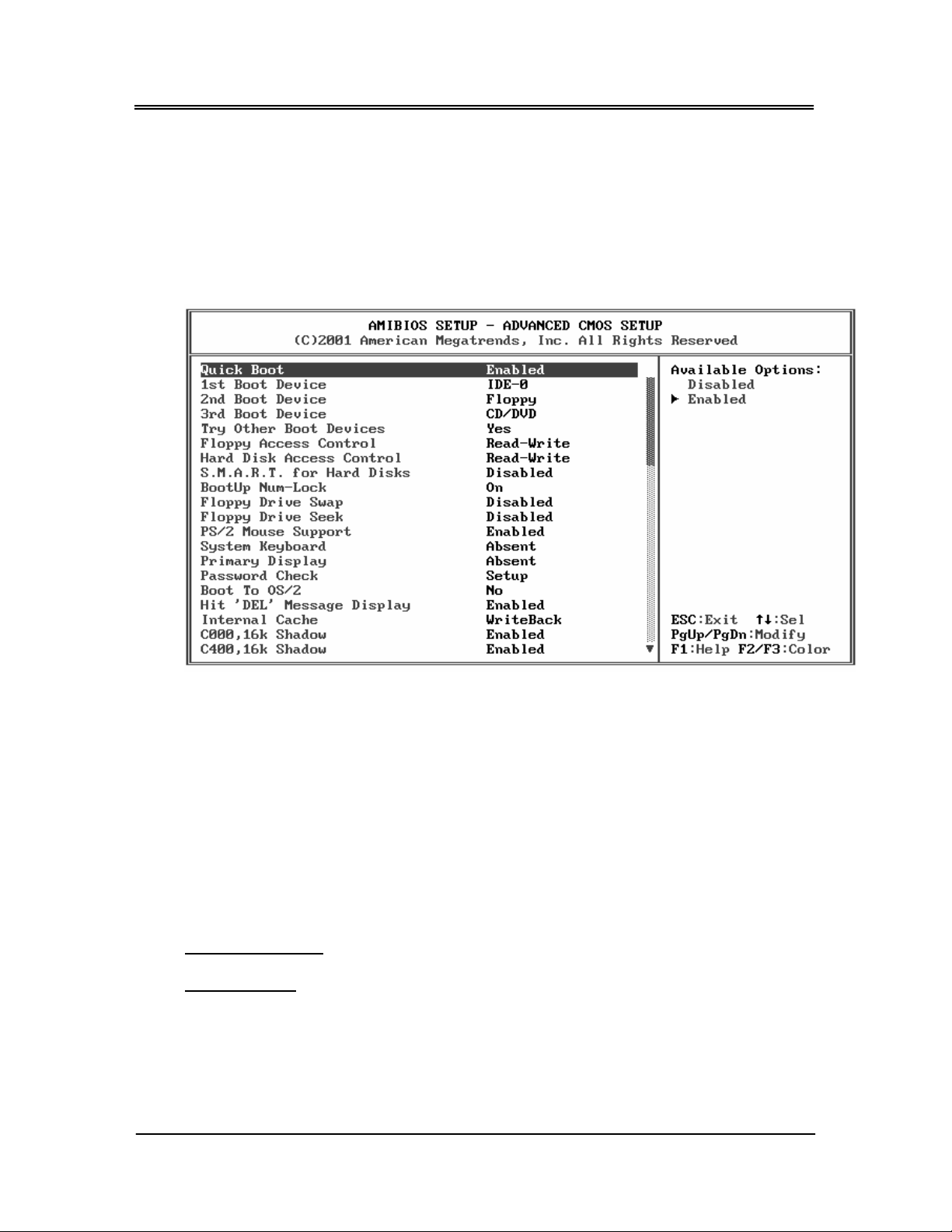
ADVANCED CMOS SETUP
This section describes the configuration entries that allow you to improve your
system performance, or let you set up some system features according to your
preference. Some entries here are required by the CPU board’s design to remain
in their default settings.
Quick Boot
This field is used to activate the quick boot function of the system. When set to
Enabled,
1. BIOS will not wait for up to 40 seconds if a Ready signal is not received from the
IDE drive, and will not configure its drive.
2. BIOS will not wait for 0.5 seconds after sending a RESET signal to the IDE drive.
3. You cannot run BIOS Setup at system boot since there is no delay for the Hit, Del.
To run Setup message.
Available Options:
Default setting:
st
1
–3rd Boot Device
Disabled, Enabled
Enabled
These fields determine where the system attempts to look for the boot drive priority
for an operating system. The default procedure is to check the hard disk, and then
the floppy drive, and last the CDROM.
30
Page 36

FabiaTech Corporation
Available options: Disabled, IDE0-1, IDE-2, IDE-3, Floppy, ARM D-FDD, ARMD-H DD,
CD/DVD, USB-FLOPPY, USB-CDROM, USB-HDD and SCSI, Network
Default setting:
IDE-0 for 1st Boot device; Floppy for 2nd Boot Device; CDROM for 3rd
Boot Device
Try Other Boot Device
If all 3 1
st
–3rd boot devices specified by CMOS setup are not available to boot,
BIOS will try to boot other available devices in following order if this question is set
to “Enable d”.
Floppy Access Control
This field specifies the read/write access when booting from a floppy drive.
Available options:
Default setting:
Normal, Read-only
Normal
Hard Disk Access Control
This field specifies the read/write access when booting from a HDD drive.
Available options:
Default setting:
Normal, Read-only
Normal
S.M.A.R.T for Hard Disk
This field is used to activate the S.M.A.R.T (System Management and Reporting
Technologies) function for S.M.A.R.T HDD drives. This function requires an
application that can give S.M.A.R.T message.
Available options:
Default:
Disabled
Disabled, Enabled
Boot Up Num-lock
This field is used to activate the Num Lock function upon system boot. If the setting
is on, after a boot, the Num Lock light is lit, and user can use the number key.
Available options:
Default setting:
On, Off
On
Floppy Drive Swap
The field reverses the drive letter assignments of your floppy disk drives in the Swap
A, B setting, otherwise leave o n the default setting of Disabled (No Swap). This
works separately from the BIOS Feat ures floppy disk swap feature. It is functionally
31
Page 37

FabiaTech Corporation
the same as physically interchanging the connectors of the floppy disk drives.
When the function’s setting is <Enabled>, the BIOS swapped floppy drive
assignments so that Drive A becomes Drive B, and Drive B becomes Drive A under
DOS.
Available options:
Default setting:
Disabled, Enabled
Disabled
Floppy Drive Seek
This field is used to set if the BIOS will seek the floppy <A> drive upon boot.
Available Options:
Default setting:
Disabled, Enabled
Disabled
PS/2 Mouse Support
The setting of Enabled allows the system to detect a PS/2 mouse on boot up. If
detected, IRQ12 will be used for the PS/2 mouse. IRQ 12 will be reserved for
expansion cards if a PS/2 mouse is not detected. Disabled will reserve IRQ12 for
expansion cards and therefore the PS/2 mouse will not function.
Available options:
Default setting:
Disabled, Enabled
Enable
System Keyboard
This field specifies if an error message should be prompted when a keyboard is not
attached.
Available options:
Default setting:
Absent, Present
Absent
Primary Display
The field specifies the type of monitor installed in the system.
Available options:
Default setting:
Absent, VGA/EGA, CGA40x25, CGA80x25, and Mono
Absent
Password Check
This field enables password checking every time the computer is powered on or
every time the BIOS Setup is executed. If Always is chosen, a user password
prompt appears every time and the BIOS Setup Program executes and the
32
Page 38

FabiaTech Corporation
computer is turned on. If Setup is chosen, the password prompt appears if the BIOS
executed.
Available options:
Default setting:
Setup, Always
Setup
Boot To OS2
If OS2 operating system is used, and the system RAM is over 64MB, please select yes.
Otherwise, select No.
Available options:
Default setting:
Yes, No
No
Hit ‘DEL’ Message Display
Set this field to Disabled to prevent the message as follows:
Hit ‘DEL’ if you want to run setup
It will prevent the message from appearing on the first BIOS screen when the
computer boots.
Available options:
Default setting:
Disabled, Enabled
Enabled
Internal Cache
This functions speeds up memory access. The STPC CPU has L1 internal cache.
Available options:
Default setting:
WriteBack, WriteThru, Disabled
WriteB ack
C000, 32k Shadow - DC00, 32k shadow
These fields control the location of the contents of the 32KB of ROM beginning at
the specified memory location. If no adapter ROM is using the named ROM area,
this area is made available to the local bus. The settings are:
1. Disabled: The video ROM is not copied to RAM. The contents of the video ROM
cannot be read from or written to cache memory.
2. Enabled: The contents of C000h - C7FFFh are written to the same address in
system memory (RAM) for faster execution.
3. Cached: The contents of the named ROM area are writte n to the same
address in system memory (RAM) for faster execution, if an adapter ROM will be
33
Page 39

FabiaTech Corporation
using the named ROM area. Also, the contents o f the RAM area can be read
from and written to cache memory.
Available options:
Default setting:
Disabled
Disabled, Enabled, Cached
34
Page 40
FabiaTech Corporation
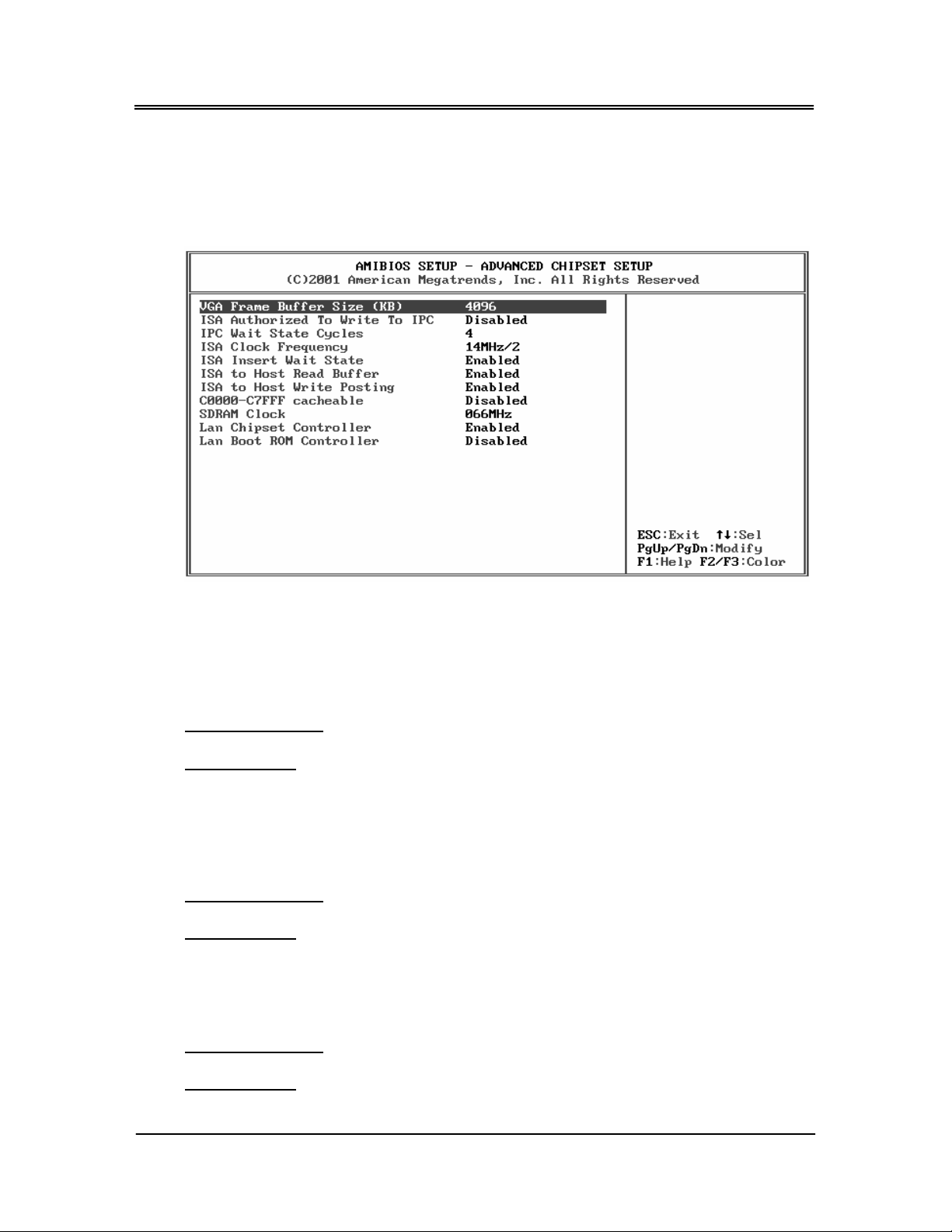
ADVANCED CHIPSET SETUP
This section describes the configuration of the board’s chipset features.
VGA Frame Buffers Size (KB)
This field is share memory architecture (SMA) for frame buffer memory. SMA allows
system memory to be efficiently share by the host CPU and allocated depending
on user preference, application requirements, and total size of system memory.
Available Options:
Default setting:
ISA Authorized To Write to IPC
This field is controls the timing of the DMA controller, and also the number of wait
state for write register to IPC.
Available Options:
Default setting:
IPC Wait State Cycle
This field is specifying the number of ISA clock wait state for read/write to IPC.
None, 128KB~4096KB
4096KB
Disabled, Enabled
Disabled
Available Options:
Default setting:
35
1, 2, 3, and 4
4
Page 41

FabiaTech Corporation
ISA Clock Frequency
This field sets the polling clock speed of ISA Bus.
Available Options:
Default setting:
PCICLK/4, and 14.318MHz/2
14.318MHz/2
ISA Insert Wait State
If selected Enable, posted writes to host memory by ISA DMA or ISA bus Master are
enabled.
Available Options:
Default setting:
Enable, and Disabled
Enabled
ISA to Host Read Buffer
If selected Enable, buffered reads of host memory by ISA DMA or ISA bus Master
are enabled.
Available Options:
Default setting:
Enable, and Disabled
Enabled
ISA to Host writer Posting
If extra wait state is inserted f or slower ISA devices, Enable is 1 wait state and
disable is 0 wait state.
Available Options:
Default setting:
Enable, and Disabled
Enabled
C0000~C7FFFF Cacheable
This field is for the 32k VGA video BIOS. Also, the contents of the RAM area can be
read from and written to cache memory.
Available Options:
Default setting:
Enable, and Disabled
Enabled
SDRAM Clock
This specifies the SDRAM memory clock frequency.
Available Options:
Default setting:
100MHz, 133MHz
100MHz
36
Page 42

FabiaTech Corporation
LAN Chipset Controller
This field specifies the Enable or Disable of the onboard LAN chip.
Available Options:
Default setting:
Disabled, Enable
Enable
LAN Boot ROM Controller
This field specifies the PXE boot ROM of the onboard LAN chip.
Available Options:
Default setting:
Disabled, Enable
Disable
37
Page 43
FabiaTech Corporation
POWER MANAGEMENT
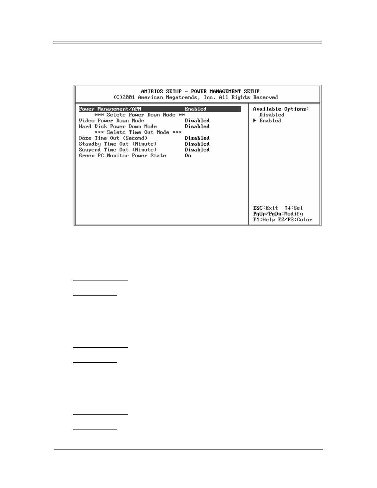
Power Management /APM
Select Enabled to activate the chipset Power Management and APM (Advanced
Power Management) features.
Available Options:
Default setting:
Video Power Down Mode
This field specifies the power conserving state that video subsystem enters after the
specified period of display inactivity has expired.
Available Options:
Default setting:
Hard Disk Power Down Mode
This field specifies the power conserving state that the hard disk drive enters after
the specified period of hard drive inactivity has expired.
Disabled, Enabled
Enabled
Disabled, Standby, Suspend
Disabled
Available Options:
Default setting:
38
Disabled, Standby, Suspend
Disabled
Page 44

FabiaTech Corporation
Standby Time Out (Minute)
This field specifies the length of a period of system inactivity (like hard disk or video)
while in full power on state. When this length of time expires, the system enters
Standby power state.
Available Options:
Disabled, 1 Minute, 2 Minute, 4 Minute, and 8 Minute, up to 60
Minute.
Default setting:
Disabled
Suspend Time Out (Minute)
This field specifies the length of a period of system inactivity (like hard disk or video)
while in Standby state. When this length of time expires, the system enters Suspend
power state.
Available Options:
Disabled, 1 Minute, 2 Minute, 4 Minute, and 8 Minute, up to 60
Minute.
Default setting:
Disabled
39
Page 45
FabiaTech Corporation
PCI/PLUG AND PLAY
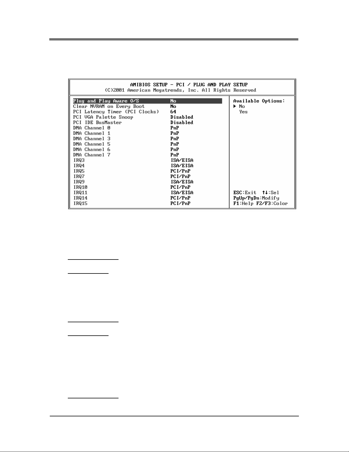
Plug and Plug Aware O/S
Set to Yes to inform BIOS that the operating system can handle Plug and Play (PnP)
devices.
Available Options:
Default setting:
PCI Latency Timer (PCI Clo cks)
This field specifies the latency timings (in PCI clock) PCI devices installed in the PCI
expansion bus.
Available Options:
Default setting:
PCI VGA Palette Snoop
When Enabled is selected, multiple VGA devices operating on different buses can
handle data from the CPU on each set of palette registers on every video device.
Bit 5 of the command register in the PCI device configuration space is the VGA
Palette Snoop bit. (0 is disabled).
Yes, No
No
32, 64, 96, 128, 160,192, 224, and 248
64
Available Options:
40
Page 46

FabiaTech Corporation
Disabled: Data read and written by the CPU is only directed to the PCI VGA
devices palette registers.
Enabled: Data read and written by the CPU is directed to both the PCI VGA
devices palette registers.
Default setting:
Disable
PCI IDE BusMaster
This option is to specify that the IDE controller on the PCI local bus have bus-mastering
capability.
Available Options:
Default setting:
Enable, Disable
Disable
DMA Channel 0 – 7
When I/O resources are controlled manually, you can assign each system DMA as
one of the following types, based on the type of device using the interrupt:
ISA/EISA devices comply with the original PC AT bus specification, requiring a
specific interrupt (Such as IRQ5 for COM1).
PnP (PCI/ISA) devices: comply with the Plug and Play standard, whether designed
for PCI or ISA bus architecture.
Available Options:
Default setting:
PnP, ISA/EISA
PnP
IRQ 3 –15
When I/O resources are controlled manually, you can assign each system interrupt
as one of the following types, based on the type of device using the interrupt:
ISA/EISA devices comply with the original PC AT bus specification, requiring a
specific interrupt (Such as IRQ5 for COM1).
PnP (PCI/ISA) devices: comply with the Plug and Play standard, whether designed
for PCI or ISA bus architecture.
41
Page 47
FabiaTech Corporation
PERIPHERAL SETUP
This section describes the function of peripheral features.
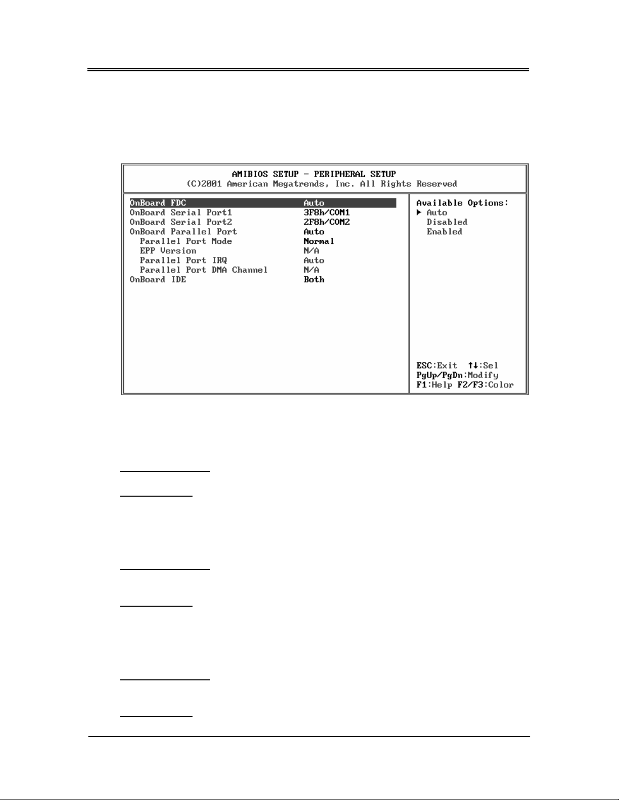
OnBoard FDC
This field enables the floppy drive controller on the FB2644.
Available Options:
Default setting:
OnBoard Serial Port 1
These fields select the I/O port address fo r each Serial port. Refer to Table 2-2.
Available Options:
2E8H/COM4.
Default setting:
OnBoard Serial Port 2
These fields select the I/O port address fo r each Serial port. Refer to Table 2-2.
Available Options:
2E8H/COM4.
Disabled, Enabled and Auto
Auto
Auto, Disabled, 3F8H/COM1, 2F8H/COM2, and 3E8H/COM3,
Auto
Auto, Disabled, 3F8H/COM1, 2F8H/COM2, and 3E8H/COM3,
Default setting:
42
Auto
Page 48

FabiaTech Corporation
OnBoard Parallel Port
This field selects the I/O port address for parallel port.
Available Options:
Default setting:
Auto, Disabled, 378, 278, and 3BCH
Auto
Parallel Port Mode
This field specifies the parallel port mode. ECP and EPP are both bi-directional
data transfer schemes that adhere to the IEEE P1284 specifications.
Available Options:
Default setting:
N/A, Normal, Bi-Dir, EPP, and ECP
Normal
EPP Version
This field specifies the EPP version for the Parallel Port Mode specification used in
the system and is not configurable. IF Normal or ECP is selected, this field displays
N/A, meaning not available.
Available Options:
Default setting:
N/A, 1.7, 1.9
N/A
Parallel Port IRQ
This field specifies the IRQ for the parallel port.
Available Options:
Default setting:
Auto, N/A, 5, 7
Auto
Parallel Port DMA Channel
This option is only available if the setting for the parallel Port Mode option is ECP.
Available Options:
Default setting:
N/A, 0,1,3
N/A
On-Board IDE
This field specifies the IDE channel that can be applied when using CN3 IDE hard
disk connector.
Available Options:
Default setting:
Disabled, Primary, and Secondary, Both
Both
43
Page 49

FabiaTech Corporation
Password Setup
There are two security passwords: Supervisor and User. Supervisor is a privileged
person that can change the User password from the BIOS.
According to the default setting, both access passwords are not set up and are
only valid after you set the password from the BIOS.
To set the password, please complete the following steps.
1. Select Change Supervisor Password.
2. Type the desired password (up to 8 character length) when you see the
message, “Enter New Supervisor Password.”
3. Then you can go on to set a user password (up to 8 character length) if
required. Note that you cannot conf igure the User password until the
Supervisor password is set up.
4. Enter Advanced CMOS Setup screen and point to the Password Checkup field.
5. Select Always or Setup.
Always: a visitor who attempts to enter BIOS or operating system will be
prompted for password.
Setup: a visitor who attempts to the operating system will be prompted for user
password. You can enter either User password or Supervisor password.
6. Point to Save Settings and Exit and press Enter.
7. Press Y when you see the message, “Save Current Settings and Exit (Y/N)?”
Note: it is suggested that you write down the password in a safe place to avoid
that password may be forgotten or missing.
To set the password, please complete the following steps.
1. Select Change Supervisor Password.
2. Press Enter instead of entering any character whe n you see the message,
“Enter New Supervisor Password.”
3. Thus you can disable the password.
44
Page 50

FabiaTech Corporation
Chapter 5 Driver and Utility
The enclosed diskette includes FB2410 LAN driver. To install and configure you
FB2410 system, you need to perform the following steps.
LAN Utility & Driver
1 To install the LAN utility OR driver, insert the CD ROM into the CD ROM
device, and enter DRIVER>LAN>RTL8139C>DIAG. If your system is not
equipped with a CD ROM device, copy the LA N driver from the CD ROM
to a CF.
2 Execute install.exe file.
Note: In the LAN directory, a HELPME.EXE file i s included to provide installation
information.
BIOS Flash Utility
In the <UTILITY> directory, there is the FLASH845.EXE file.
Step 1: Use the FLASH845.EXE program to update the BIOS setting.
Step 2: And then refer to the chapter “BIOS Setup”, as the steps to modify BIOS.
Step 3: Now the CPU board’s BIOS loaded with are the newest program; user can
use it to modify BIOS function in the future, when the BIOS add some
functions.
45
Page 51

FabiaTech Corporation
Watchdog Timer
This section describes how to use the Watchdog Timer, including disabled, enabled,
and trigg e r f u n ctions.
The FB2410 is equipped with a programmable time-o ut period watchdog timer.
You can use your own program to enable the watchdog timer. Once you have
enabled the watchdog timer, the program should trigger the I/O every time before
the timer times out. If your program fails to trigger or disable this timer before it
times out, e.g. because of a system hang-up, it will generate a reset signal to reset
the system. The time-out period can be programmed to b e s et from 1 to 255
seconds or minutes.
Time Base
ADD.(A0-A15)
Watchdog
Register
Counter
Data(D)-D7)
and
Compartor
Watchdog
LED
RESET
The CD –ROM includes a Watch Dog demo file. In the file, there are 3 execution
programs written in different forms. The sub-directories of the file are:
1. WATCHDOG/SMSc787/ASSEMBLE: Library and Test Program written in Assembly
Language
2. WATCHDOG/SMSc787/TURBOC: Library and Test Program written in Turbo C
The WATCHDOG includes a demonstration program established for users who
would like to configure the Watchdog timer by themselves.
Note: In the WATCHDOG directory, README.TXT file is included to provide demo
program information.
++
46
Page 52

FabiaTech Corporation
Watchdog Timer Setting
The watchdog timer is a circuit that may be used from your program software to
detect system crashes or hang-ups. LED1 on this CPU board is the watchdog timer
indicator, which is located at the upper-right corner above the USB connector.
Whenever the watchdog timer is enabled, the LED will blink to indicate that the
timer is counting. The watchdog timer is automatically disabled after reset.
Once you have enabled the watchdog timer, your program must trigger the
watchdo g timer eve ry time before it times out. After you trigger the watchdog
timer, it will be set to non-zero value to w atchdog c ounter and start to count down
again. If your program fails to trigger the watchdog timer before time-out, it will
generate a reset pulse to reset the system.
The factor of the watchdog timer time-out constant is approximately 1 seconds.
The period for the watchdog timer time-out is be tw een 1 to FF tim e r f a ctors.
If you want to reset your system when watchdog times out, the following table
listed the relation of timer factors between time-out periods.
Time Factor
(Seconds)
(Minutes)
1 1 1
2 2 2
3 3 3
4 4 4
5 5 5
“ “ “
“ “ “
“ “ “
FF FF FF
Time-Out Period Time-Out Period
47
Page 53

FabiaTech Corporation
Watchdog Timer Enabled
To enable the watchdog timer, you have to output a byte of timer factor to the
++
watchdog. The following is a Turbo C
program, which demonstrates how to
enable the watchdog timer and set the time-out period at 6 seconds.
#include “stdio.H”
#include “WDLIB.H”
main( )
{
char WD_TIME=ox6;
InitWD(equWdUnitS);
printf (“Enable watchdog”);
//Trigger watchdog Timer Output is 6 seconds
EnWD(WD_TIME);
}
Watchdog Timer Trigger
After you enable the watchdog timer, your program must write the same factor as
enabling to the watchdog register at least once every time-out period to its
previous setting. You can change the time-out period by writing another timer
factor to the watchdog register at any time, and you must trigger the watchdog
++
before the new time-out period in the next trigger. Below is a Turbo C
program,
which demonstrates how to trigger the watchdog timer:
#include “stdio.H”
#include “WDLIB.H”
main( )
{
char WD_TIME=ox6;
InitWD(equWdUnitS);
printf (“Enable watchdog”);
//Trigger watchdog Timer Output is 6 seconds
EnWD(WD_TIME);
}
48
Page 54

FabiaTech Corporation
Watchdog Timer Disabled
To disable the watchdog timer, simply write a 0 0H to the watchdog register.
#include “stdio.H”
#include “WDLIB.H”
main( )
{
InitWD(equWdUnitS);
printf (“Disable Watch Dog”);
//Disable watch dog
DisWD(WD_TIME);
}
49
Page 55

FabiaTech Corporation
50
Page 56

FabiaTech Corporation
Chapter 6 Technical Reference
This section outlines the errors that may occur when yo u operate the system,
and also gives you the suggestions on solving the problems.
Topic include:
z Trouble Shooting for Post Beep & Error Messages
z Technical Reference
z How to configuration I/O port resource
Trouble Shooting for Post Beep and Error Messages
The following information informs the Post Beep & error messages. Please adjust
your systems according to the messages below. Make sure all the components
and connectors are in proper position and firmly attached. If the errors still exist,
please contact with your distributor for maintenance.
¾ POST BEEP
Currently there are two kinds of beep codes in B IOS setup.
z One indicates that a video error has occurred and the BIOS cannot initialize
the video screen to display any additional information. This beep code
consists of a single long beep f ollowed by three short beeps.
z The other indicates that an error has occurred in your DRAM. This beep code
consists of a constant single long beep.
¾ Error Message
CMOS BATTERY FAILURE
When the CMOS battery is out of work or has run out, the user has to replace it with
a new battery.
51
Page 57

FabiaTech Corporation
CMOS CHECKSUM ERROR
This error informs that the CMOS has corrupted. When the battery runs weak, this
situation might happen. Please ch eck the battery and change a new one when
necessary.
DISK BOOT FAILURE
When you can‘t find the boot device, insert a system disk into Drive A and press <
Enter >. Make sure both the controller and cables are all in proper positions, and
also make sure the disk is formatted. Then reboot the system.
DISKETTE DRIVES OR TYPES MISMATCH ERROR
When the diskette drive type is different from CMOS, please run setup or configure
the drive again.
ERROR ENCOUNTERED INITIALIZING HARD DRIVE
When you can‘t initializes the hard drive, ensure the following things:
1. The adapter is installed correctly
2. All cables are correctly and firmly attached
3. The correct hard drive type is selected in BIOS Setup
ERROR INITIALIZING HARD DISK CONTROLLER
When this error occurs, ensure the following things:
1. The cord is exactly installed in the bus.
2. The correct hard drive type is selected in BIOS Setup
3. Whether all of the jumpers are set correctly i n the hard drive
KEYBOARD ERROR OR NO KEYBOARD PRESENT
When this situation happens, please check keyboard attachment and no keys
being pressed during the boot. If you are purposely configuring the system without
a keyboard, set the error halt condition in BIOS Setup to HALT ON ALL, BUT
KEYBOARD. This will cause the BIOS to ignore the missing keyboard and continue
the boot procedure.
MEMORY ADDRESS ERROR
When the memory address indicates error, you can use this location along with the
memory map for your system to find and replace the bad memory chips.
52
Page 58

FabiaTech Corporation
MEMORY SIZE HAS CHANGED
Memory has been added or removed since last boot. In EISA mode, use
Configuration Utility to re-configure the memory configuration. In ISA mode enter
BIOS Setup and enter the new memory size in the memory fields.
MEMORY VERIFYING ERROR
It indicates an error verifying a value is already written to memory. Use the location
along with your system's memory map to locate the bad chip.
OFFENDING ADDRESS MISSING
This message is used in connection with the I/O CHANNEL CHECK and RAM PARITY
ERROR messages when the segment that has caused the problem cannot be
isolated.
REBOOT ERROR
When this error occurs that requires you to reboot. Press any key and the system
will reboot.
SYSTEM HALTED
Indicates the present boot attempt has been aborted and the system must be
rebooted. Press and hold down the CTRL and ALT keys and press DEL.
53
Page 59

FabiaTech Corporation
Technical Reference
¾ Physical and Environmental
Temperature: Operating 0°C ~ 60°C
Relative humidity 5 % to 95 % non-condensing
¾ Real-Time Clock and Non-Volatile RAM
The FB2410 contains a real-time clock compartment that maintains the date and
time in addition to storing configuration information about the computer system. It
contains 14 bytes of clock and control registers and 114 bytes of general purpose
RAM. Because of the use of CMOS technology, it consumes very little power and
can be maintained for long periods of time using an internal Lithium battery. The
contents of each byte in the CMOS RAM are listed below:
Address Description
00 Seconds
01 Second alarm
02 Minutes
03 Minute alarm
04 Hours
05 Hour alarm
06 Day of week
07 Date of month
08 Month
09 Year
0A Status register A
0B Status register B
0C Status register C
0D Status register D
0E Diagnostic status byte
0F Shutdown status byte
10 Diskette drive type byte, drive A and B
11 Fixed disk type byte, drive C
54
Page 60

FabiaTech Corporation
Address Description
12 Fixed disk type byte, drive D
13 Reserved
14 Equipment byte
15 Low base memory byte
16 High base memory byte
17 Low expansion memory byte
18 High expansion memory byte
19-2D Reserved
2E-2F 2-byte CMOS checksum
30 Low actual expansion memory byte
31 High actual expansion memory byte
32 Date century byte
33 Information flags (set during power on)
34-7F Reserved fo r system BIOS
55
Page 61

FabiaTech Corporation
¾ CMOS RAM Map
Register Description
00h -10h Standard AT-compatible RTC and Status and Status
Register data definitions
11h – 13h Varies
14h Equipment
Bits 7-6 Number of Floppy Drives
00 1 Drive
01 2 Drives
Bits 5-4 Monitor Type
00 Not CGA or MDA 01 40x25 CGA
01 2 Drives 80x25 CGA
Bits 3 Display Enabled
0 Disabled
1 Enabled
Bit 2 Keyboard Enabled
00 Not CGA or MDA 01 40x25 CGA
01 2 Drives 80x25 CGA
Bit 1 Math Coprocessor Installed
0 Absent
1 Present
Bit 0 Floppy Drive Installed
0 Disabled
1 Enabled
15h Base Memory (in 1KB increments), Low Byte
16h Base Memory (in 1KB increments), High Byte
17h IBM-compatible memory (in 1KB incremen ts), Low Byte
18h IBM-compatible memory (in 1KB increments), High
Byte (max 15 MB)
19h-2Dh Vaires
2Eh Standard CMOS RAM checksum, high byte
2Fh Standard CMOS RAM checksum, low byte
30h IBM-compatible Extended Memory, Low Byte (POST) in
KB
31h IBM-compatible Extended Memory, High Byte (POST)
in KB
32h Century Byte
33h Reserved. Do not use
34h Reserved. Do not use
35h Low byte of extended memory (POST) in 64 KB
36h High byte of extended memory (POST) in 64 KB
37h-3Dh Varies
3Eh Extended CMOS Checksum, Low Byte (including 34h-
3Dh)
3Fh Extended CMOS Checksum, High Byte (including 34h-
3Dh)
56
Page 62

FabiaTech Corporation
¾ I/O Port Address Map
Each peripheral device in the system is assigned a set of I/O port addresses, which
also becomes the identity of the device. There is a total of 1K-port address space
available. The following table lists the I/O port addresses used on the Industrial CPU
Card.
Address Device Description
000h - 01Fh DMA Controller #1
020h - 03Fh Interrupt Controller #1
040h - 05Fh Timer
060h - 06Fh Keyboard Controller
070h - 073h Real Time Clock, NMI
080h - 09Fh DMA Page Register
0A0h - 0BFh Interrupt Controller #2
0C0h - 0DFh DMA Controller #2
0F0h Clear Math Coprocessor Busy Signal
0F1h Reset Math Coprocessor
1F0h - 1F7h IDE Interface
290h – 297h System Chipset
2E8h – 2EFh Serial Port #4(COM4)
2F8h - 2FFh Serial Port #2( COM 2)
2B0 - 2DF Graphics adapter Controller
378h - 3FFh Parallel Port #1(LPT1)
360 - 36F Network Ports
3B0 - 3BF Monochrome & Printer adapter
3C0 - 3CF EGA adapter
3D0 - 3DF CGA adapter
3E8h – 3EFh Serial Port #3(COM3)
3F0h - 3F7h Floppy Disk Controller
3F8h - 3FFh Serial Port #1( COM 1)
57
Page 63

FabiaTech Corporation
¾ Interrupt Request Lines (IRQ)
There are a total of 15 IRQ lines available on the Industrial CPU Card. Peripheral
devices use interrupt request lines to notify CPU for the service required. The
following table shows the IRQ used by the devices on the Industrial CPU Card.
Level Function
IRQ0 System Timer Output
IRQ1 Keyboard
IRQ2 Interrupt Cascade
IRQ3 Serial Port #2
IRQ4 Serial Port #1
IRQ5 USB
IRQ6 Floppy
IRQ7 - Reserved IRQ8 Real Time Clock
IRQ9 - Reserved IRQ10 - Reserved IRQ11 LAN #1
IRQ12 PS2 Mouse
IRQ13 FPU
IRQ14 Primary IDE
IRQ15 - Reserved -
58
Page 64

FabiaTech Corporation
¾ Serial Ports
The ACEs (Asynchronous Communication Elements ACE1 to ACE2) are used to
convert parallel data to a serial format on the transmit side and convert serial data
to parallel on the receiver side. The serial format, in order of transmission and
reception , is a start b it, followed by five to eight data bits, a parity bit (if
programmed) and one, one and half (five-bit format only) or two stop bits. The
ACEs are capable of handling divisors of 1 to 65535, and produce a 16x clock for
driving the internal transmitter logic.
Provisions are also included to use this 16x clock to drive the receiver logic. Also
included in the ACE a completed M O DEM control capability, and a processor
interrupt system that may be software tailored to the computing time required to
handle the communications link.
The following table is a summary of each ACE accessible register
DLAB Port Address Register
Receiver buffer (read) 0 Base + 0
Transmitter holding register (write)
0 Base + 1 Interrupt enable
X Base + 2 Interrupt identification (read only)
X Base + 3 Line control
X Base + 4 MODEM control
X Base + 5 Line status
X Base + 6 MODEM status
X Base + 7 Scratched register
1 Base + 0 Divisor latch (least significant byte)
1 Base + 1 Divisor latch (most significant byte)
Receiver Buffer Register (RBR)
Bit 0-7: Received data byte (Read Only)
Transmitter Holding Register (THR)
Bit 0-7: Tr ansmitter holding data byte (Write Only)
Interrupt Enable Register (IER)
Bit 0: Enable Received Data Available Interrupt (ERBFI)
59
Page 65
FabiaTech Corporation
Bit 1: Enable Transmitter Holding Empty Interrupt (ETBEI)
Bit 2: Enable Receiver Line Status Interrupt (ELSI)
Bit 3: Enable MODEM Status Interrupt (EDSSI)
Bit 4: Must be 0
Bit 5: Must be 0
Bit 6: Must be 0
Bit 7: Must be 0
Interrupt Identification Register (IIR)
Bit 0: “0” if Interrupt Pending
Bit 1: Interrupt ID Bit 0
Bit 2: Interrupt ID Bit 1
Bit 3: Must be 0
Bit 4: Must be 0
Bit 5: Must be 0
Bit 6: Must be 0
Bit 7: Must be 0
Line Control Register (LCR)
Bit 0: Word Length Select Bit 0 (WLS0)
Bit 1: Word Length Select Bit 1 (WLS1)
WLS1 WLS0 Word Length
0 0 5 Bits
0 1 6 Bits
1 0 7 Bits
1 1 8 Bits
Bit 2: Number of Stop Bit (STB)
Bit 3: Par ity Enable (PEN)
Bit 4: Even Parity Select (EPS)
60
Page 66

FabiaTech Corporation
Bit 5: Stick Parity
Bit 6: Set Break
Bit 7: Di visor Latch Access Bit (DLAB)
MODEM Control Register (MCR)
Bit 0: Data Terminal Ready (DTR)
Bit 1: Request to Send (RTS)
Bit 2: Out 1 (OUT 1)
Bit 3: Out 2 (OUT 2)
Bit 4: Loop
Bit 5: Must be 0
Bit 6: Must be 0
Bit 7: Must be 0
Line Status Register (LSR)
Bit 0: Data Ready (DR)
Bit 1: Overrun Error (OR)
Bit 2: Parity Error (PE)
Bit 3: Framing Error (FE)
Bit 4: Break Interrupt (BI)
Bit 5: Transmitter Holding Register Empty (THRE)
Bit 6: Transmitter Shift Register Empty (TSRE)
Bit 7: Must be 0
MODEM Status Register (MSR)
Bit 0: Delt a C l e a r to Send (DC TS)
Bit 1: Delta Data Set Ready (DDSR)
Bit 2: Training Edge Ring Indicator (TERI)
Bit 3: Delta Receive Line Signal Detect (DSLSD)
61
Page 67
FabiaTech Corporation
Bit 4: Clear to Send (CTS)
Bit 5: Data Set Ready (DSR)
Bit 6: Ring Indicator (RI)
Bit 7: Received Line Signal Detect (RSLD)
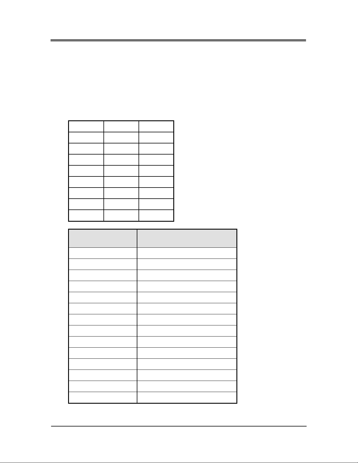
Divisor Latch (LS, MS)
LS MS
Bit 0: Bit 0 Bit 8
Bit 1: Bit 1 Bit 9
Bit 2: Bit 2 Bit 10
Bit 3: Bit 3 Bit 11
Bit 4: Bit 4 Bit 12
Bit 5: Bit 5 Bit 13
Bit 6: Bit 6 Bit 14
Bit 7: Bit 7 Bit 15
Desired Baud
Rate
300 384
600 192
1200 96
1800 64
2400 48
3600 32
4800 24
9600 12
14400 8
19200 6
28800 4
Divisor Used to Generate 16x
Clock
38400 3
57600 2
115200 1
62
Page 68
FabiaTech Corporation
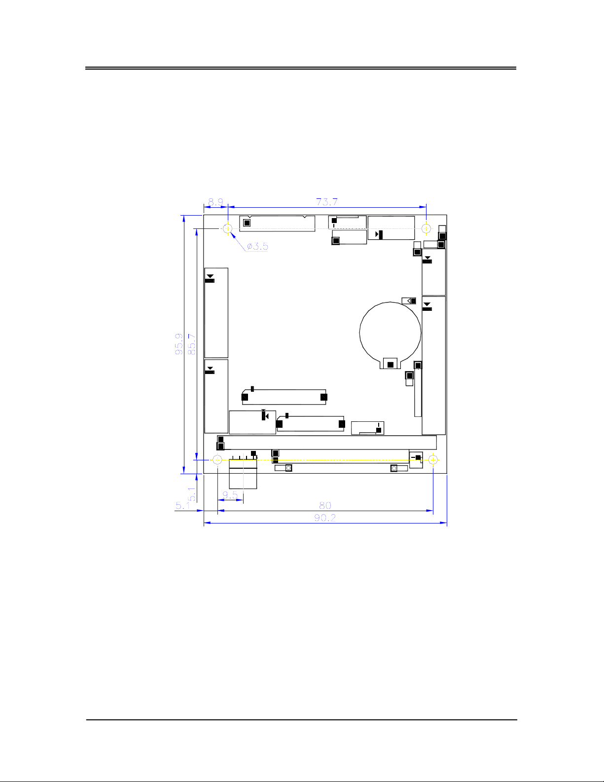
Dimension
Appendix
63
 Loading...