

Page 1

WD-MSO
2.4GHz/5GHz
WLAN(IEEE 802.11a/b/g/n)
Stand-alone Module
Page 2

TABLE OF CONTENTS
1. APPLICATION ................................................................................................................................................................... 3
2. QUALITY ........................................................................................................................................................................... 3
3. APPEARANCE AND CHARACTERISTICS ...................................................................................................................... 3
3.1 A
3.2 C
PPEARANCE ..................................................................................................................................................................................................... 3
HARACTERISTICS ............................................................................................................................................................................................. 3
4. APPLICATION OF 2.4GHZ/5GHZ WLAN(802.11A/B/G/N) STAND-ALONE MODULE ......................................... 3
5. ABSOLUTE MAXIMUM RATING .................................................................................................................................... 3
6. TEST ................................................................................................................................................................................... 3
7. MECHANICAL DIMENSION ........................................................................................................................................... 4
8. GENERAL DESCRIPTION ................................................................................................................................................ 5
9. EXTERNAL CLOCK REFERENCE ..................................................................................................................................... 5
9.1 E
XTERNAL LPO SIGNAL REQUIREMENT ....................................................................................................................................................... 5
10. INPUT/OUTPUT DC TERMINAL CHARACTERISTICS ................................................................................................. 5
11. ELECTRICAL CHARACTERISTICS ................................................................................................................................... 5
11.1 O
11.2 2.4GH
11.3 2.4G
11.4 5GH
11.5 5GH
PERATING CONDITION .................................................................................................................................................................................. 5
Z TX CHARACTERISTICS ....................................................................................................................................................................... 6
HZ RX CHARACTERISTICS ....................................................................................................................................................................... 6
Z TX CHARACTERISTICS .......................................................................................................................................................................... 7
Z RX CHARACTERISTICS .......................................................................................................................................................................... 7
12. PIN ASSIGNMENT (TOP VIEW, BOTTOM LAYER)...................................................................................................... 8
13. PIN DESCRIPTION ........................................................................................................................................................... 9
14. BLOCK DIAGRAM .......................................................................................................................................................... 10
15. POWER SEQUENCE ....................................................................................................................................................... 11
16. REVISION HISTORY ...................................................................................................................................................... 11
17. Warni n gn Statements ……………………………………………………………………………….…………………..…11
Page 3
1. Application
This specification is applied to the 2.4GHz/5GHz WLAN(802.11a/b/g/n) Stand-Alone module of
BIXOLON
2. Quality
Quality should meet each condition which are mentioned on this specification. However, items which are not
mentioned on this specification should f ol low the insp e c tion agreements and standards which are agre ed w ith
both companies.
3. Appearance and Characteristics
3.1 Appearance
Appearance should not be contaminated by harmful materials and have cracks etc.
Mechanical dimension should meet the contents of clause 7.
3.2 Characteristics
Electrical characteristics should meet the contents of clause 12.
4. Applic a t ion of 2.4GHz/5GHz WLAN(802.11a/b/g/n) Stand-Alone Module
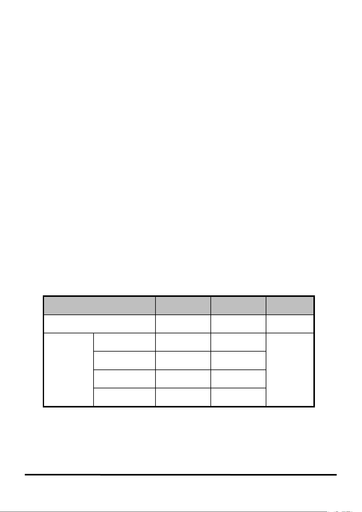
WD-MSO is a 2.4GHz/5Ghz WLAN(802.11a/b/g/n) Stand-Alone Module for IoT(Internet of Things) such as
Home electronic appliance, Room controller, Smart plug, etc. But, this module is not designed for Life Support
Application.
Also it is recommended that this module should be mounted by reflow soldering.
5. Absolute Maximum Rating
Min. Max. Unit
Storage Te mperature -40 +85 deg.C
VBAT_A, B -0.5 +4.6
Supply
Voltage
VDDIO_1,2,RF -0.5 +4.0
V
VDD_MEM -0.5 +4.0
VDD_FEM -0.3 +5.0
6. Test
Electrical characteristics are tested for every product. However, if there are any objections in judgment,
it should be treated with agreements of companies.
3
Page 4
Dimension
mm× mm × mm(Max.)
7. Mechanical Dimension
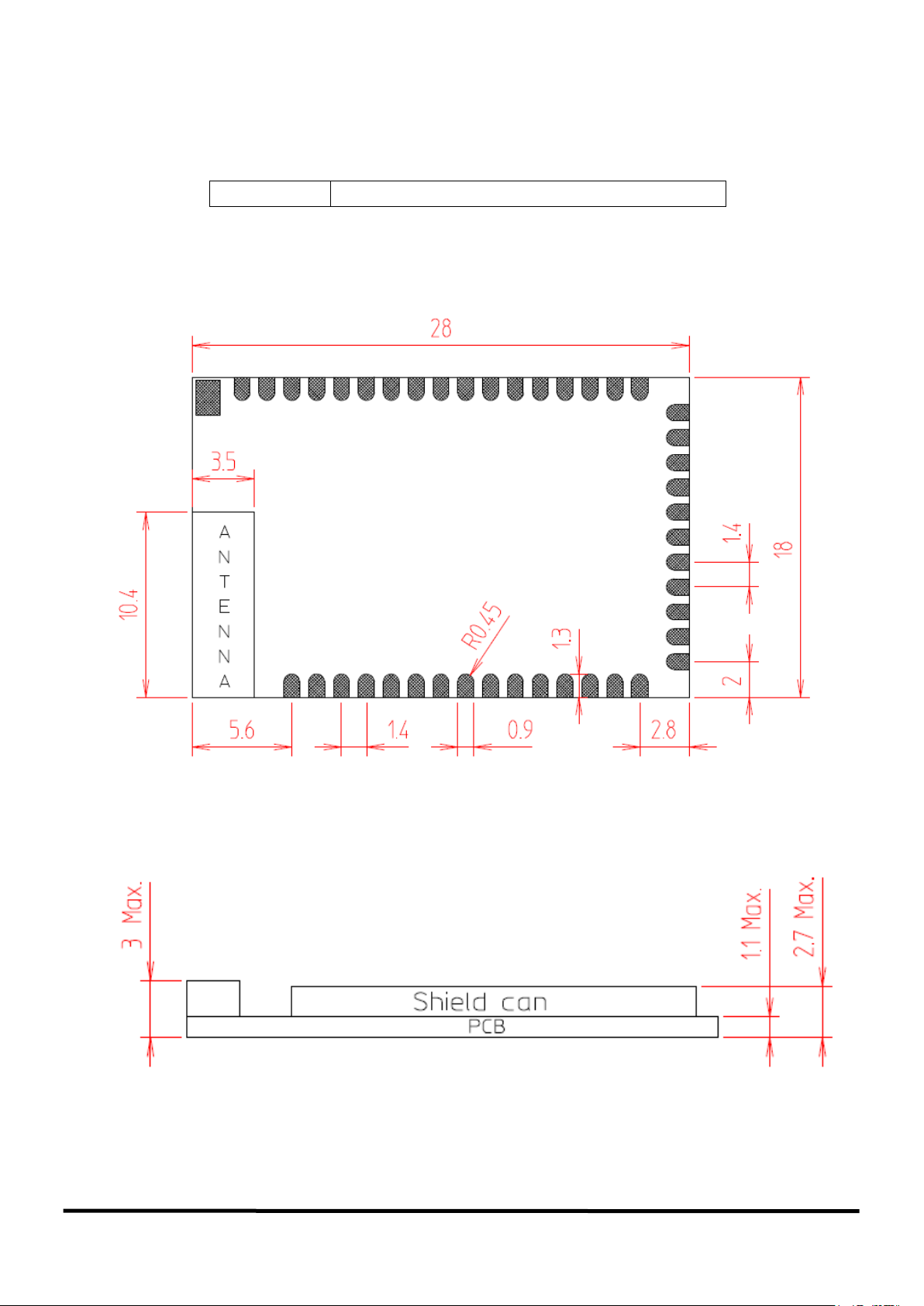
Figure 1 and Figure 2 show the Bottom Layer (Top View) and the side dimension of WD-MSO package
outline
Figure 1. Package Outline (Top View)
Figure 2. Package Outline (Side View)
4
Page 5
Parameters
External LPO Clock
Unit
Nominal input frequency
32.768
kHz
Frequency accuracy
±200
ppm
Input signal amplitude*
VDDIO
mVp-p
Signal type
Square-wave or sine-wave
-
> 100k
< 5 When power is applied or power is off
Ω
pF
Min.
Typ.
Max.
Unit
VDD_MEM
3.0
3.3
3.6
VDD_FEM
3.2
3.6
4.4
8. Gener a l De s cr iption
WD-MSO is a compact size and low power System-in-Package (SiP) for 2.4GHz/5GHz WLAN(802.11a/b/g/n)
aimed at embedded and IOT applications.
WD-MSO can be available as 3~46 pin. ( 28mm x 18mm x Max. 3.0mm )
9. External Clock Reference
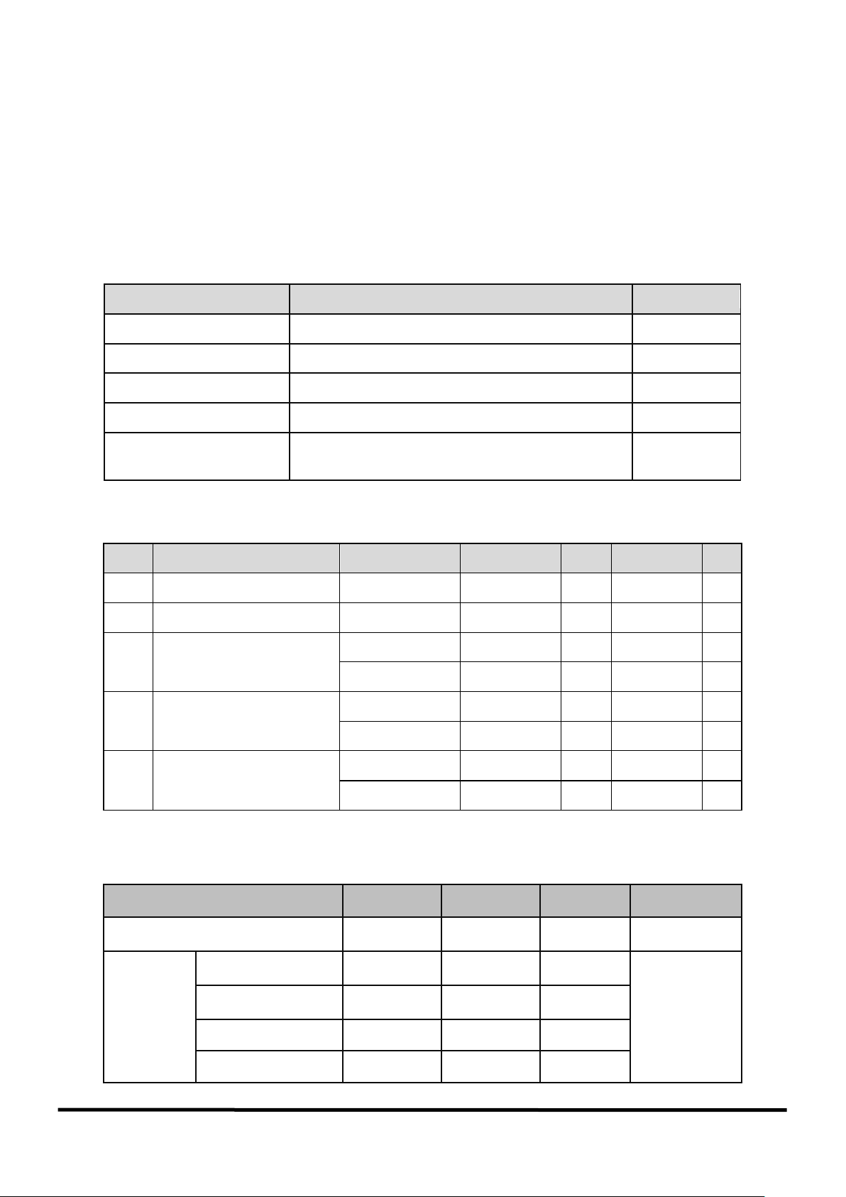
9.1 External LPO Signal Requirement
Input impedance
10. Input/ O ut put DC Term inal Characteristics
VIH High Level Input Voltage VDDIO=3.3V 0.7xVDDIO
VIL Low Level Input Voltage VDDIO=3.3V
VOH High Level Output Voltage
Parameters Conditions Min. Typ. Max. Unit
@100uA, 3.3V VDDIO-0.3
@2mA, 3.3V VDDIO-0.35
@100uA, 3.3V
VOL Low Level Output Voltage
@2mA, 3.3V
CIN Input Capacitance
11. Electrical Characteristics
11.1 Operating Condition\
V
0.3xVDDIO V
V
V
0.4 V
0.4 V
5 pF
Operating Te mperature -30 25 +85 deg.C
VBAT_A,B 3.3 3.6 4.5
Supply
Voltage
VDDIO_1,2,RF 3.0 3.3 3.6
V
5
Page 6
* The optimal RF performance specified in this datasheet is guaranteed for temperatures from -20℃~+70℃
Spec.
Min.
Typ.
Max.
Unit
Frequency Range
2400
-
2500
MHz
CCK, 1 Mbps
-96.5
CCK, 2 Mbps
-94.5
CCK, 5.5 Mbps
-92.5
CCK, 11 Mbps
-89.5
OFDM, 6 Mbps
-93.5
OFDM, 9 Mbps
-91.5
OFDM, 12 Mbps
-90.5
OFDM, 18 Mbps
-88.5
OFDM, 24 Mbps
-86.5
OFDM, 36 Mbps
-82.5
OFDM, 48 Mbps
-79.5
OFDM, 54 Mbps
-77.5
HT20, MCS0
-93.5
HT20, MCS1
-89.5
HT20, MCS2
-87.5
HT20, MCS3
-84.5
HT20, MCS4
-81.5
HT20, MCS5
-77.5
HT20, MCS6
-76.5
HT20, MCS7
-74.5
Adjacent
CCK, 1 Mbps (signal; -74dBm)
35
-
dB
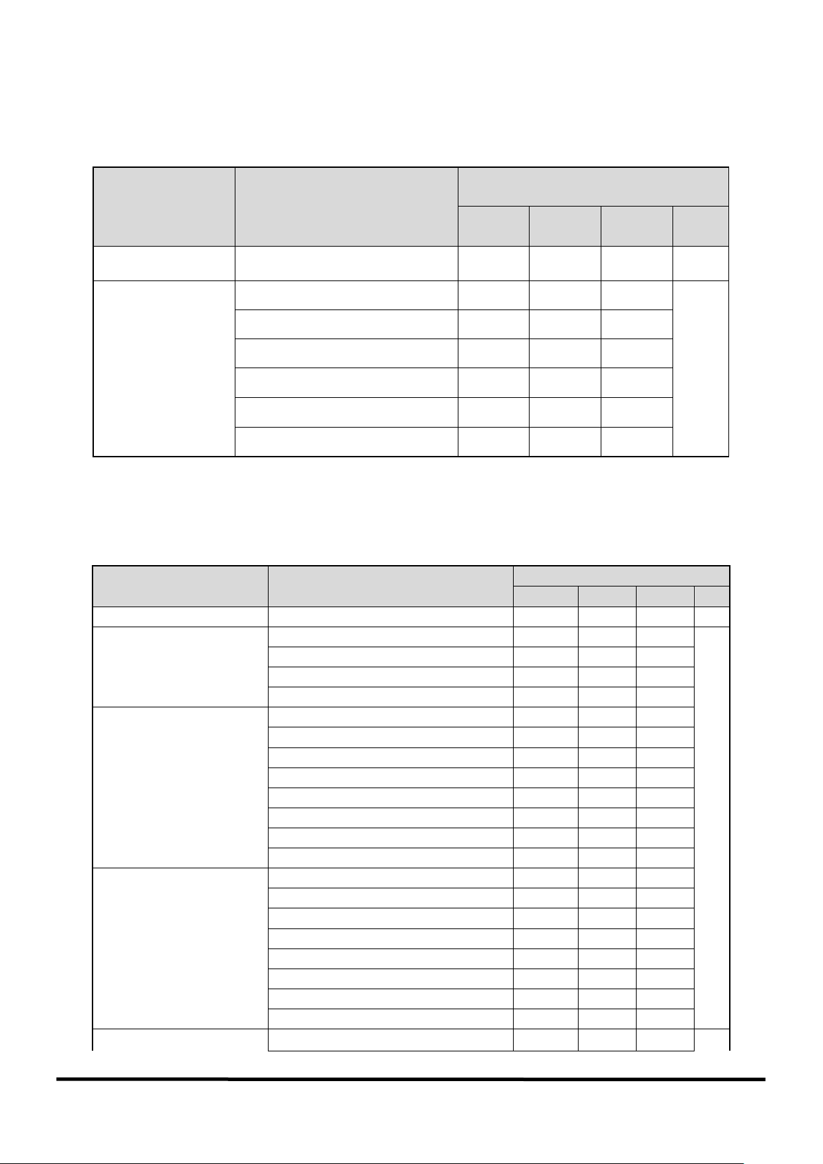
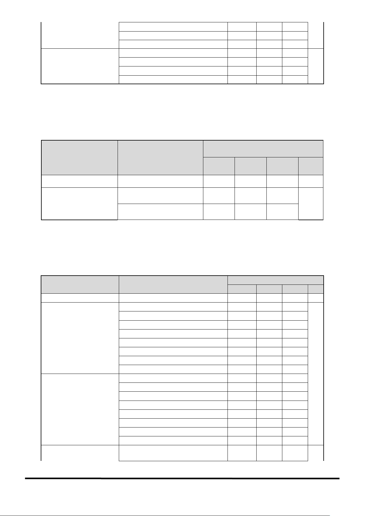
11.2 2.4GHz Tx Characteristics
All measurements are made under nominal supply voltage,
(VBAT_A,B = 3.3V, VDDIO_1,2, RF=3.3V, VDD_MEM=3.3V) and room temperature (25℃)condition.
Spec.
Parameters Conditions
Min. Typ. Max. Unit
Frequency Range
Output Power
(VBAT=3.3V,
spectral mask,
EVM compliance)
11.3 2.4Ghz Rx Characteristics
All measurements are made under nominal supply voltage,
(VBAT_A,B = 3.3V, VDDIO_1,2, RF=3.3V, VDD_MEM=3.3V) and room temperature (25℃)condition.
Parameters Conditions
11b, Rx Sensitivity
(8% PER for 1024 octet
PSDU)
802. 11b, EVM = -9 dB
OFDM , BPSK, EVM = -8 dB
OFDM, QPSK, EVM = -13 dB
OFDM, 16QAM, EVM = -19 dB
OFDM, 64QAM
OFDM, 64QAM
3/4
, EVM = -25 dB
5/6
, EVM = -28 dB
2400 - 2500 MHz
16.5
15
15
dBm
15
13
13
11g, Rx Sensitivity
(10% PER for 1024 octet
PSDU)
11n, Rx Sensitivity
(10% PER for 4096 octet
PSDU)
dBm
6
Page 7
Channel Rejection
CCK, 11 Mbps (signal; -70dBm)
35
-
OFDM, 6 Mbps (signal; -79dBm)
16
-
OFDM, 54 Mbps (signal; -62dBm)
-1
-
Max Input level
11b 1M,2M
0
11b 5.5M, 11M
0
11g
-10
11n
-10
Output Power
EVM compliance)
11a, OFDM, 64QAM 3/4,
EVM = -25 dB
11n, OFDM, 64QAM 5/6,
EVM = -28 dB
Spec.
Min.
Typ.
Max.
Unit
Frequency Range
4900
-
5845
MHz
OFDM, 6 Mbps
-92.5
OFDM, 9 Mbps
-90.5
OFDM, 12 Mbps
-89.5
OFDM, 18 Mbps
-87.5
OFDM, 24 Mbps
-84.5
OFDM, 36 Mbps
-81.5
OFDM, 48 Mbps
-77.5
OFDM, 54 Mbps
-76
HT20, MCS0
-91.5
HT20, MCS1
-89.5
HT20, MCS2
-86
HT20, MCS3
-83
HT20, MCS4
-80
HT20, MCS5
-75.5
HT20, MCS6
-73.5
HT20, MCS7
-73
Adjacent
Channel Rejection
11a, OFDM, 54Mbps
(Signal : -62dBm)
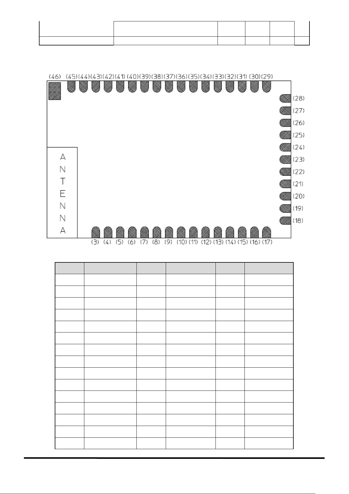
11.4 5GHz band Tx Characteristics
All measurements are made under nominal supply voltage,
(VBAT_A,B = 3.3V, VDDIO_1,2, RF =3.3V, VDD_MEM =3.3V, VDD_FEM=3.3V) and room temperature
(25℃)condition
Parameters Conditions
dBm
Spec.
Min. Typ. Max. Unit
Frequency Range
(VBAT, VDD_FEM=3.3V,
spectral mask,
11.5 5GHz Rx Cha racter istics
All measurements are made under nominal supply voltage,
(VBAT_A,B = 3.3V, VDDIO_1,2, RF =3.3V, VDD_MEM =3.3V, VDD_FEM=3.3V) and room temperature
(25℃)condition
Parameters Conditions
11a, Rx Sensitivity
(10% PER for 1024 octet
PSDU)
4900 - 5845 MHz
13
dBm
13
11n, Rx Sensitivity
(10% PER for 4096 octet
PSDU)
7
dBm
-1
dBm
Page 8
11n, HT20, MCS7
(Signal : -61dBm)
Max Input level
11a/n
-20
dBm
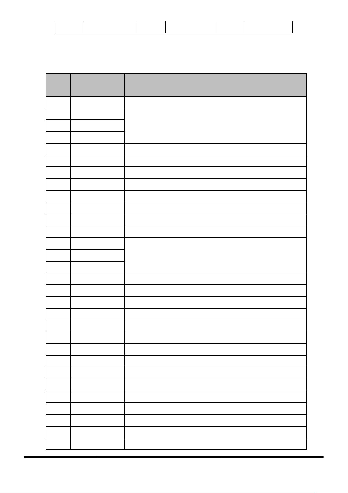
No.
Pin Name
No.
Pin Name
No.
Pin Name
3
GND
19
GP12
35
SD_D1
4
GND
20
GND
36
GND
5
GND
21
GP13
37
SPI_MISO
6
GND
22
VBAT_B
38
SPI_CS
7
VDDIO_1
23
CLK_RTC
39
GND
8
RSTN
24
GP09
40
GP11
9
GP14
25
GP08
41
GP10
10
SF_SEL
26
NC
42
GND
11
VDDIO_2
27
NC
43
GND
12
JTAG_SEL
28
VDD_MEM
44
N/C
13
VDDIO_RF
29
GND
45
GND
14
VBAT_A
30
SD_D2
46
GND
15
GND
31
SD_D3
16
GND
32
SD_CMD
17
GND
33
SD_CLK
12. Pin Assignment (Top View, Bottom Layer)
-2
8
Page 9
18
PMIC_EN
34
SD_D0
Pin
3
GND
4
GND
5
GND
6
GND
7
VDDIO_1
GP5~GP15 IO PWR(JTAG, SDIO etc)
8
RSTN
RESET input
9
GP14
Factory Reset input, Before 5GHz LNA Control output
10
SF_SEL
Serial Flash boot select
11
VDDIO_2
GP5~GP15 IO PWR(JTAG, SDIO etc)
12
JTAG_SEL
JTAG Debug select
13
VDDIO_RF
GP00/GP01 IO PWR(Internal RF SW control)GP02/GP03 IO PWR
14
VBAT_A
Internal 1.4V DC_DC POWER input(3.3V~4.7V)
15
GND
16
GND
17
GND
18
PMIC_EN
INTERNAL PMIC PWR EN
19
GP12
UART2 TXD/GPIO
20
GND
UART2 CTS/GPIO
21
GP13
UART2 RXD/GPIO
22
VBAT_B
Internal 2.5V LDO, 3.3V LDO POWER input(3.3V~4.7V)
23
CLK_RTC
Low speed clock input
24
GP09
UART0 RXD/GPIO
25
GP08
UART0 TXD/GPIO
26
NC
Not connected (Internal SF_SIO0)
27
NC
Not connected (Internal SF_SCLK)
28
VDD_MEM
Internal Flash Memory Power input
29
GND
Module Ground
30
SD_D2
SDIO Data 2
31
SD_D3
SDIO Data 3/SDIO SPI Mode CS
32
SD_CMD
SD CMD/SDIO SPI Mode DI
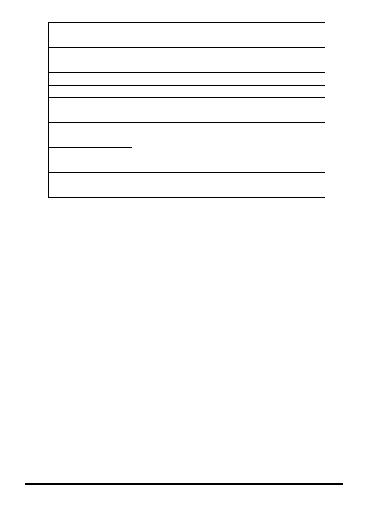
13. Pi n De s cription
Num.
Pin Name Description
Module Ground
Module Ground
9
Page 10
33
SD_CLK
SDIO Clock (~50 MHz)/SDIO SPI Mode CLK(~50MHz)
34
SD_D0
SD Data 0/SDIO SPI Mode DO
35
SD_D1
SD Data 1/SDIO SPI Mode IRQ
36
GND
Module Ground
37
GP05
SPI_MISO
38
GP07
SPI_CS
39
GND
Module Ground
40
GP11
UART1 TXD/GPIO
41
GP10
UART1 RXD/GPIO
42
GND
43
GND
44
NC
Not connected
45
GND
46
GND
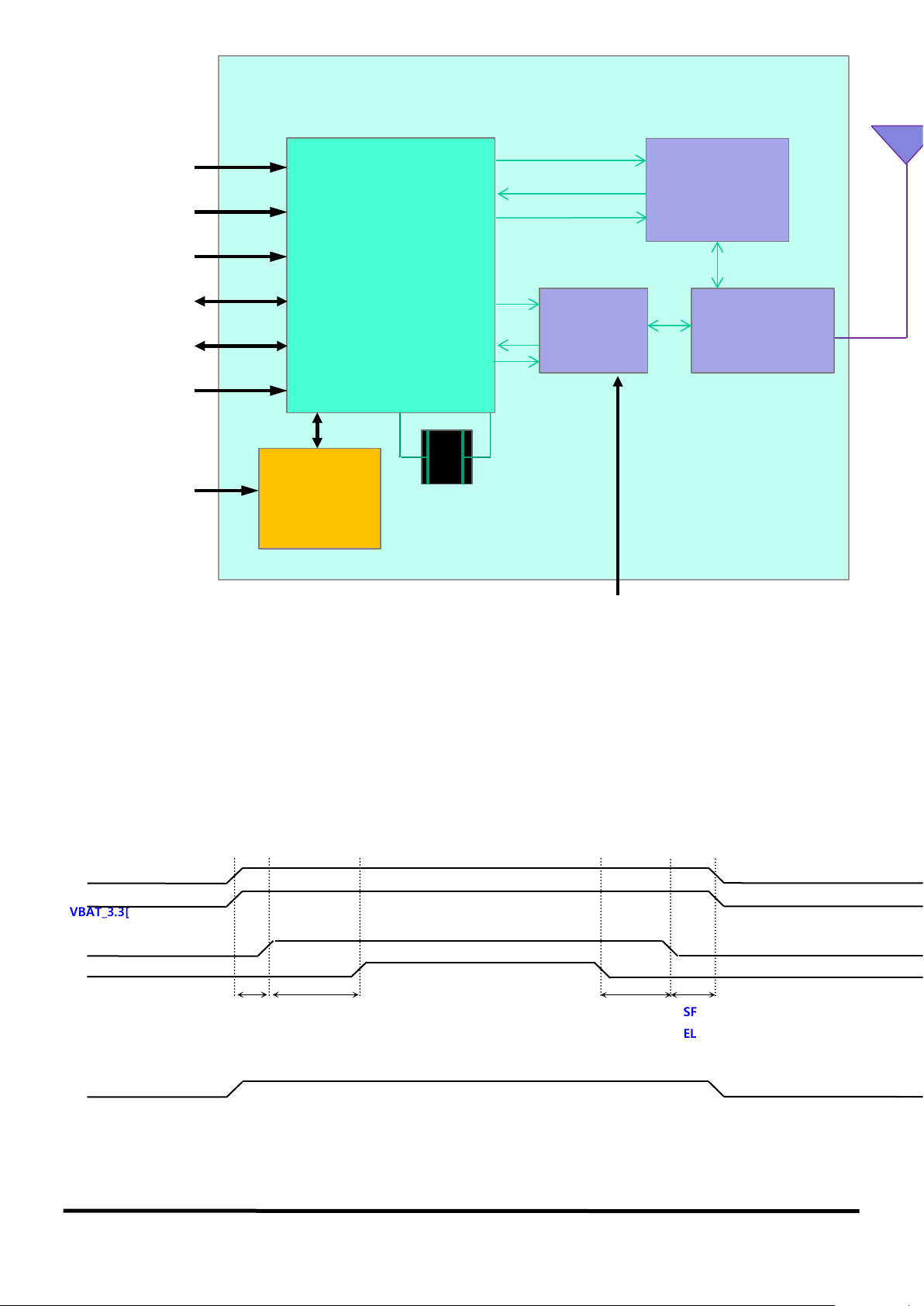
14. Block Diagram
Module Ground
Module Ground
10
Page 11
VBAT
VDDIO
VDDIO_RF
Shield CAN
WF5000
Tx
Rx
control
2.4/5G
Chip A
2.4GHz
Switch
GPIO/UART
SDIO/SPI
CLK_RTC
VDD_MEM
Wi-Fi Chip
Serial
Flash
(32Mbit)
Tx
Rx
control
Ref CLK
(40MHz)
Figure 3. Block Diagram
5GHz
DIPLEXER
FEM
VDD_FEM
15. Power Sequence
VDDIO_3
.3[V]
VBAT_3.3[V]~4.7[V]
PMIC_EN
RESET
Min
10uS
※ When VCC is below 3.0V, it must be reset.
Min
10mS
Min
10uS
SF_S
EL
Power
down
11
Page 12

16. Revision History
Ver.
Comment
Date
Author
Approver
0.1
Initial release
Nov,18,2016
Y.S.SEO
17. Warning Statements
<FCC Warning Statements>
FCC Part 15.19 Statements:
This device complies with Part 15 of the FCC Rules. Operation is subject to the following two conditions: (1) this
device may not cause harmful interference, and (2) this device must accept any interference received, including
interference that may cause undesired operation.
FCC Part 15.105 statement
This equipment has been tes ted and f ound to com pl y with the l im its for a Class B digital device, p ursuant t o part 15 of
the FCC Rules.
These limits are desi gned to provide reasonable prot ection against harmful interf erence in a residential installation.
This equipment gener ates, uses and can ra diate rad io frequenc y energy and, if not ins talled and us ed in ac cordance
with the instructio ns, may cause harmful interf erence to radio comm unications. However, there is no guarantee th at
interference will not occur in a particular installation. If this equipment does cause harmful interference to radio or
television reception, which can be determined by turn ing the equipment off and on, the user is enc ouraged to try to
correct the interference by one or more of the following measures:
- Reorient or relocate the receiving antenna.
- Increase the separation between the equipment and receiver.
- Connect the equipment into an outlet on a circuit different from that to which the receiver is connected.
- Consult the dealer or an experienced radio/TV technician for help.
FCC Part 15.21 statement
Any changes or m odifications not express ly approved by the part y responsible for com pliance could void the user 's
authority to operate this equipment.
RF Exposure Statement
The antenna(s) must be installed such that a minimum separation distance of at least 20 cm is
maintained between the radiator (antenna) and all persons at all times. This device must not be co-located or
operating in conjunction with any other antenna or transmitter.
End Product Labeling
The module is labeled with its own FCC ID and IC Certification Number. If the FCC ID and IC
Certification Number are not visible when the module is installed inside another device, then the
outside of the device into which the module is installed must also display a label referring to the
enclosed module. In that case, the final end product must be labeled in a visible area with the
following:
12
Page 13

“Contains FCC ID: 2AKMF-WD-MSO”
“Contains IC: 22266-WDMSO”
RSS-GEN, Sec. 8.4– (licence-exempt radio apparatus)
This device com plies with Indus try Canada licence-exempt RSS stan dard(s). O peration is subjec t to the foll owing two
conditions:
(1) this device may not cause interference, and
(2) this device must accept any interference, including interference that may cause undesired operation of the device.
Le présent appareil est c onforme aux CNR d’Industrie Can ada applicables aux appareils radio exempts de licence.
L’exploitation est autorisée aux deux conditions suivantes :
(1) l’appareil ne doit pas produire de brouillage, et
(2) l’utilisateur d e l’appareil doit acc epter tout brouillage ra dioélectrique subi, m ême si le brouillage est susceptible
d’en compromettre le fonctionnement.
RF Exposure
The antenna (or antennas) must be installed so as to maintain at all times a distance minimum of at least 20 cm
between the radiation s ource (antenna) and any ind ividual. This device ma y not be installed or used in co njunction
with any other antenna or transmitter.
l'exposition aux RF
L’antenne (ou les antennes) doit être installée de f açon à maintenir à tout instant une dista nce minim um de au moins
20 cm entre la source de radiation (l’antenne) et toute personne physique.
Étiquetage du produit final (IC)
Le module BT111 est étiqueté avec sa propre identification FCC et son propre numéro de
certification IC. Si l’identification FCC et le numéro de certification IC ne sont pas visibles lorsque
le module est installé à l’intérieur d’un autre dispositif, la partie externe du dispositif dans lequel
le module est installé devra également présenter une étiquette faisant référence au module inclus.
Dans ce cas, le produit final devra être étiqueté sur une zone visible avec les informations
suivantes :
« Contient module émetteur identification FCC ID : 2AKMF-WD-MSO
« Contient module émetteur IC : 22266-WDMSO
13
 Loading...