


1
Edition 1.3
July 2004
FLD5F20NP-D
FEATURES
• Modulator Integrated DFB Laser Diode Module
• CW operation of DFB laser section
• Available at C Band ITU-T grid wavelengths between
1529.55 - 1563.05nm
• Modulation voltage applied only to modulator section
• High speed butterfly package with GPO connection
• Built-in optical isolator, monitor photodiode, thermistor, and
thermo-electric cooler
APPLICATION
This MI laser is intended for intermediate reach applications (≤40km)
at 10Gb/s.
DESCRIPTION
The Modulator Integrated DFB Laser (MI DFB Laser) has an electro-absorption modulator
monolithically integrated with a conventional Distributed Feed-Back (DFB) laser. The modulation
voltage is applied to the modulator section while the laser section operates CW allowing extremely low
wavelength chirping. Extinction ratios of more than 10 dB can be achieved with 2.6 Vp-p modulation.
The MI laser is installed in a butterfly type package. The module incorporates a highly stable optical
coupling system. The module includes an optical isolator, monitor photodiode, thermistor and a
thermo-electric cooler.
Parameter Symbol
Storage Temperature
T
stg
+85-
°C
-40
Operating Case Temperature
+70-
°C
T
op
-20
Optical Output Power
5CW mW
P
f
-
Laser Forward Current
150CW mA
I
F
-
Laser Reverse Voltage
2CW V
V
R
-
Modulator Forward Voltage
+1CW V
V
m
-5
Photodiode Forward Current
1-mA--
10-V
Photodiode Reverse Voltage
V
DR
-
10260°C sec
Lead Soldering Time
--
TEC Voltage
+2.5Cooling
-Heating
V
V
c
-
-2.5
TEC Current
+1.4Cooling
-Heating
A
I
c
-
-0.9
Thermistor Temperature
+70-20ATC Operation °CTth
Rating
Unit
Min. Max.
ABSOLUTE MAXIMUM RATINGS (Top=25°C, unless otherwise specified)
Condition
1,550nm Modulator
Integrated DFB Laser
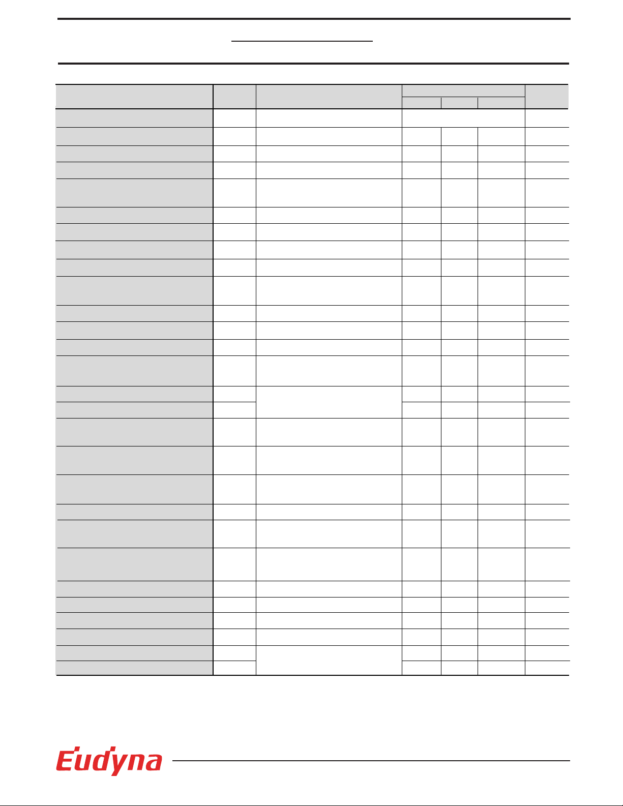
Parameter Symbol
OPTICAL & ELECTRICAL CHARACTERISTICS (TL= T
set, Tc
= 25°C, BOL, unless otherwise specified)
Unit
Limits
Max.TypeMin.
Test Condition
Laser Set Temperature (BOL)
Tset °C3515 -
Note (2)
Peak Wavelength
λ
p
Note (4)
RF Return Loss
S
11
dB
8- -
f=DC-5GHz, 50Ω Test Set,
Vm=Vo, IF=I
op
RF Return Loss
S
11
dB
5- -
f=5-10GHz, 50Ω Test Set,
Vm=Vo, IF=I
op
Cut-off Frequency
S
21
GHz
10 - -
-3dB bandwidth,
Vm=Vo-0.5|Vmod|, IF=I
op
Optical Output Power
(Avg. Power)
Pf dBm--2.0 -
Wavelength Drift (after 20 years)
-nm0.1-0.1 -
Wavelength Stability
with Case Temperature
-pm/°C±0.5--
Dispersion Penalty
dP dB2--
Note (1)
Sidemode Suppression Ratio
SSR dB-35 -Note (2)
Note (2)
Forward Voltage
V
F
V- 2.01.4
CW, IF=Iop, Vm=Vo
Optical Isolation
I
s
dB-25 35Tc=-20 to +70°C
TEC Power Dissipation
P
c
W3.3--
IF=I
op
Thermal Resistance
R
th
kΩ
10.59.5 10.0
TL=25°C , Tc=+25°C
Thermistor B Constant (Note 3)
BK3,6303,270 3,450
In-Band Ripple
∆G
dB
-
±1.0
-
IF=I
op, f=0.1-10GHz,
Vm=Vo-0.5|Vmod|
Threshold Current
I
th
mA-30-
CW, Vm=Vo
On Level Modulation
V
o
V-0.7 0--
Modulator Drive Voltage
V
mod
V- 2.6-(Vo-Vmod)≥-3.3V, Rext=10dB
Relative Intensity Noise
RIN dB/Hz- -120-
f=10 MHz to 8.5 GHz,
Vm=Vo, IF=I
op, 8% Reflection
Operating Current
I
op
mA40 100--
Monitor Current
I
m
mA0.04 1.5-Note (2), VDR=5V
Extinction Ratio
R
ext
dB--10
f=10Gb/s, IF=Iop,
Vm=Vo/(Vo-Vmod)
Rise Time
T
r
ps25-20
Fall Time
T
f
ps25-20
Note (2), 20 to 80%
Note (1) Eudyna Test System
9.95328Gb/s, PRBS=2
23
-1, IF=Iop, Vm=Vo and (Vo-Vmod)
Dispersion=800ps/nm, Dispersion penalty at
Bit Error Rate = 1.0E-10
Note (2) Eudyna Test System
9.95328Gb/s, PRBS=2
23
-1, IF=Iop, Vm=Vo and (Vo-Vmod)
Note (3) Relation between resistance and temperature (°K) is:
Rth (T) = Rth (25°C)*exp[B(1/T-1/298)]
Note (4) Reference Figure 7 for Wavelength Table
TEC Capacity
∆T
°C-70-Tset -
P
TEC
=3.3W, IF=I
op
TEC Current
I
c
A1.3--
IF=I
op,
∆T=(70-Tset)[°C]
TEC Voltage
V
c
V2.5--
IF=I
op,
∆T=(70-Tset)[°C]
2
FLD5F20NP-D
1,550nm Modulator
Integrated DFB Laser
3
FLD5F20NP-D
10Gb/s
PRBS=223-1
IF=I
op
Vm=Vo/(Vo-2)
Vo=-0.3V
TLD=25°C
P
f
I
m
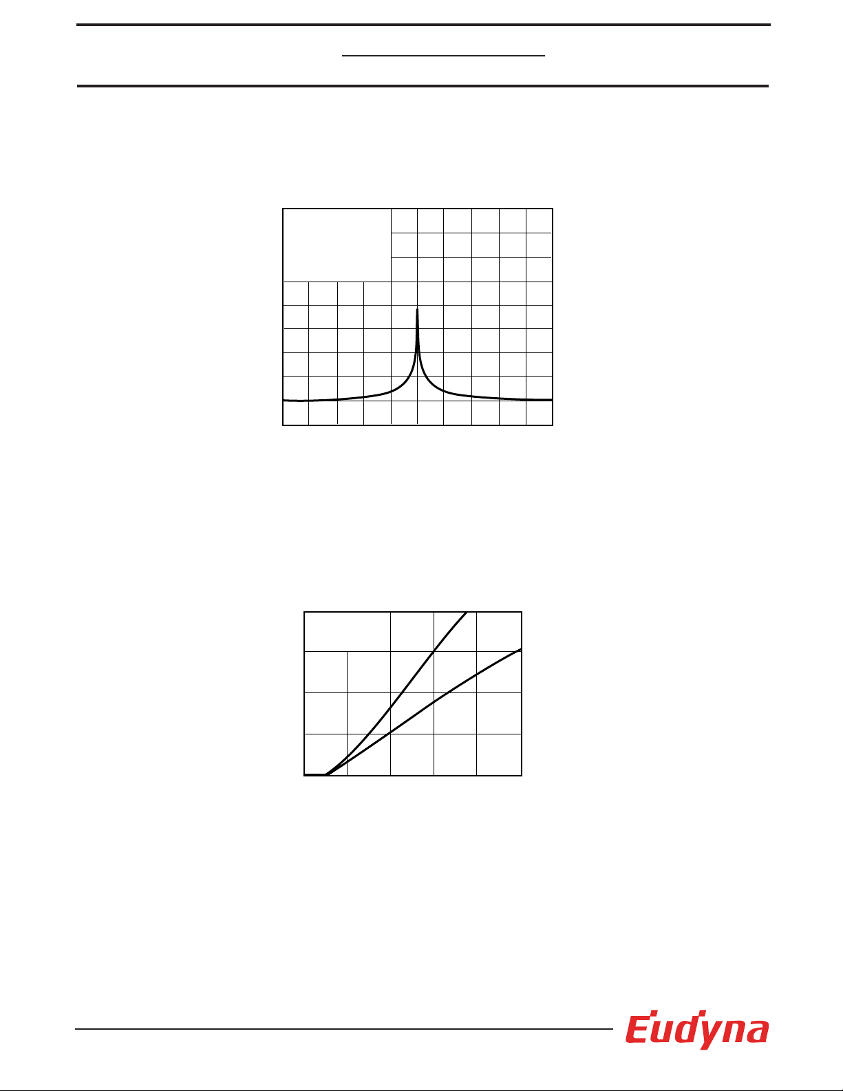
Fig. 1 Lasing Spectrum
Wavelength (Span=1 nm/div, Res.=0.1nm)
Fig. 2 Output Power & Monitor Current
vs. Forward Current
Forward Current, IF (mA)
Output Power, P
f
(mW)
Monitor Current, I
m
(mA)
3
4
2
1
20 40 60 80 1000
0
0.75
1.0
0.5
0.25
0
Relative Intensity (10 dB/div.)
1,550nm Modulator
Integrated DFB Laser
4
FLD5F20NP-D
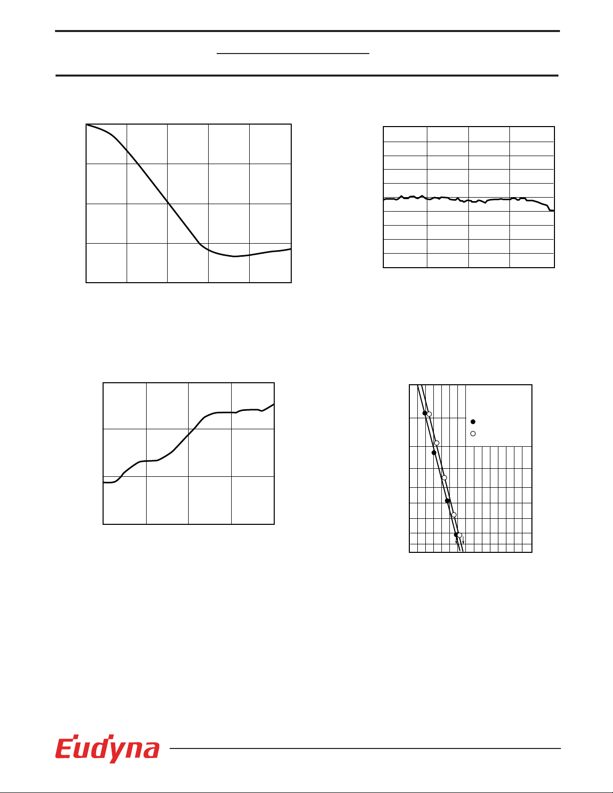
Fig. 6 Transmission Characteristics
9.95328Gb/s
PRBS=2
23
-1
0 km
800ps/nm
Average Received Optical
Power (dBm)
Bit Error Rate
10
-12
10
-10
10
-8
10
-6
10
-4
-15 -10
Fig. 3 Extinction Ratio vs.
Modulation Applied Voltage
Fig. 4 Cut-off Frequency (S21)
Frequency, f (GHz)
Modulation Applied Voltage (V)
Extinction Ratio (dB)
Relative Output (dB)
-10
-5
0
-15
-20
0.5 1.0 1.5 2.0 2.50
51015200
-12
-9
-6
-3
0
3
6
9
12
Fig. 5 RF Return Loss (S11)
Frequency, f (GHz)
Return Loss (dB)
51015200
-30
-20
-10
0
1,550nm Modulator
Integrated DFB Laser
5
FLD5F20NP-D
1,550nm Modulator
Integrated DFB Laser
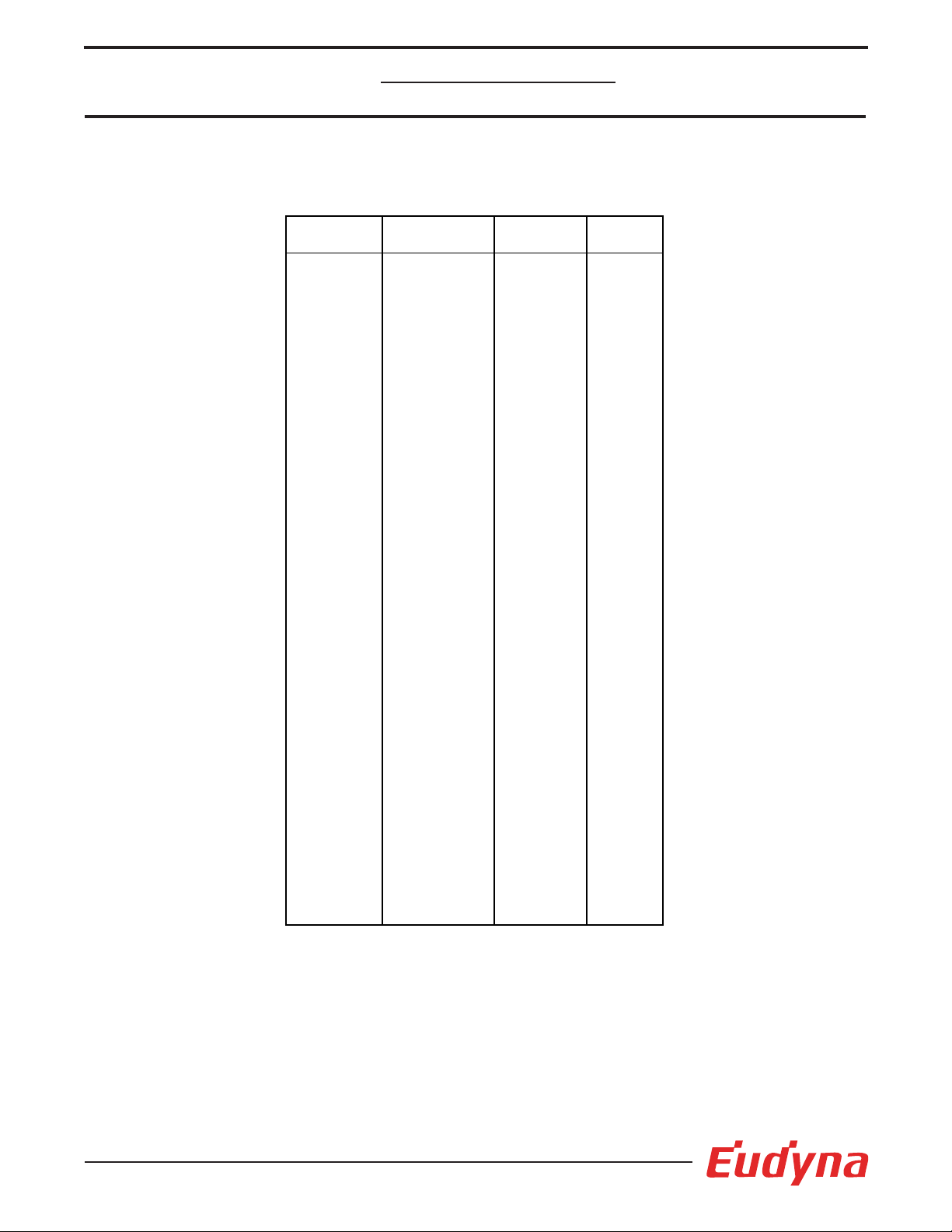
Figure 7 Wavelength Table
Wavelength (nm)
Part Number
FLD5F20NP-D60 1529.55 196.00 ±0.1
FLD5F20NP-D59 1530.33 195.90 ±0.1
FLD5F20NP-D58 1531.12 195.80 ±0.1
FLD5F20NP-D57 1531.90 195.70 ±0.1
FLD5F20NP-D56 1532.68 195.60 ±0.1
FLD5F20NP-D55 1533.47 195.50 ±0.1
FLD5F20NP-D54 1534.25 195.40 ±0.1
FLD5F20NP-D53 1535.04 195.30 ±0.1
FLD5F20NP-D52 1535.82 195.20 ±0.1
FLD5F20NP-D51 1536.61 195.10 ±0.1
FLD5F20NP-D50 1537.40 195.00 ±0.1
FLD5F20NP-D49 1538.19 194.90 ±0.1
FLD5F20NP-D48 1538.98 194.80 ±0.1
FLD5F20NP-D47 1539.77 194.70 ±0.1
FLD5F20NP-D46 1540.56 194.60 ±0.1
FLD5F20NP-D45 1541.35 194.50 ±0.1
FLD5F20NP-D44 1542.14 194.40 ±0.1
FLD5F20NP-D43 1542.94 194.30 ±0.1
FLD5F20NP-D42 1543.73 194.20 ±0.1
FLD5F20NP-D41 1544.53 194.10 ±0.1
FLD5F20NP-D40 1545.32 194.00 ±0.1
FLD5F20NP-D39 1546.12 193.90 ±0.1
FLD5F20NP-D38 1546.92 193.80 ±0.1
FLD5F20NP-D37 1547.72 193.70 ±0.1
FLD5F20NP-D36 1548.51 193.60 ±0.1
FLD5F20NP-D35 1549.32 193.50 ±0.1
FLD5F20NP-D34 1550.12 193.40 ±0.1
FLD5F20NP-D33 1550.92 193.30 ±0.1
FLD5F20NP-D32 1551.72 193.20 ±0.1
FLD5F20NP-D31 1552.52 193.10 ±0.1
FLD5F20NP-D30 1553.33 193.00 ±0.1
FLD5F20NP-D29 1554.13 192.90 ±0.1
FLD5F20NP-D28 1554.94 192.80 ±0.1
FLD5F20NP-D27 1555.75 192.70 ±0.1
FLD5F20NP-D26 1556.56 192.60 ±0.1
FLD5F20NP-D25 1557.36 192.50 ±0.1
FLD5F20NP-D24 1558.17 192.40 ±0.1
FLD5F20NP-D23 1558.98 192.30 ±0.1
FLD5F20NP-D22 1559.79 192.20 ±0.1
FLD5F20NP-D21 1560.61 192.10 ±0.1
FLD5F20NP-D20 1561.42 192.00 ±0.1
FLD5F20NP-D19 1562.23 191.90 ±0.1
FLD5F20NP-D18 1563.05 191.80 ±0.1
(TL=Tset)
(in vacuum)
Frequency
(THz)
Tolerance (nm)
6
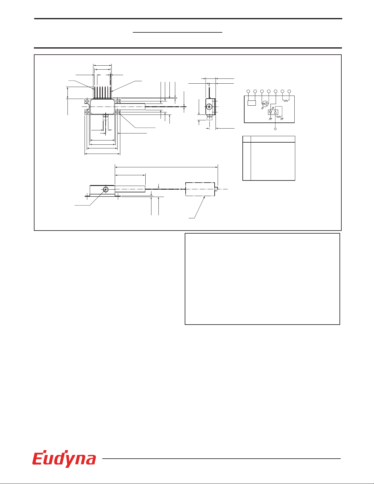
FLD5F20NP-D
“NP” PACKAGE
UNIT: mm
1,550nm Modulator
Integrated DFB Laser
Eudyna Devices Inc. products contain gallium arsenide
(GaAs) which can be hazardous to the human body and the environment.
For safety, observe the following procedures:
CAUTION
• Do not put this product into the mouth.
• Do not alter the form of this product into a gas, powder, or liquid
through burning, crushing, or chemical processing as these by-products
are dangerous to the human body if inhaled, ingested, or swallowed.
• Observe government laws and company regulations when discarding this
product. This product must be discarded in accordance with methods
specified by applicable hazardous waste procedures.
For further information please contact:
Eudyna Devices USA Inc.
2355 Zanker Rd.
San Jose, CA 95131-1138, U.S.A.
TEL: (408) 232-9500
FAX: (408) 428-9111
www.us.eudyna.com
Eudyna Devices Europe Ltd.
Network House
Norreys Drive
Maidenhead, Berkshire SL6 4FJ
United Kingdom
TEL: +44 (0) 1628 504800
FAX: +44 (0) 1628 504888
Eudyna Devices Asia Pte Ltd.
Hong Kong Branch
Rm. 1101, Ocean Centre, 5 Canton Rd.
Tsim Sha Tsui, Kowloon, Hong Kong
TEL: +852-2377-0227
FAX: +852-2377-3921
Eudyna Devices Inc.
Sales Division
1, Kanai-cho, Sakae-ku
Yokohama, 244-0845, Japan
TEL: +81-45-853-8156
FAX: +81-45-853-8170
Eudyna Devices Inc. reserves the right to change products and specifications
without notice. The information does not convey any license under rights of
Eudyna Devices Inc. or others.
© 2004 Eudyna Devices USA Inc.
Printed in U.S.A.
PIN 7
8.25±0.20
2.54±0.20
PIN 8
17.24±0.25
15.24±0.25
ø4.16
20.83±0.25
22.00±0.25
26.04±0.25
29.97±0.25
7-0.5
PIN 1
4-ø2.67±0.2
10.0±0.25
25.0±0.5
0.5±0.2
8.89±0.15
ø5.2±0.25
5.47±0.2
1.25
12.7±0.25
*L
CONNECTOR
ø0.9±0.1
7-0.15±0.05
4.83±0.20
8.17±0.25
5.41±0.25
5.08±0.25
TOP VIEW
7685432
TEC
# PIN DESIGNATIONS
1 Thermistor
2 Thermistor
3 LD Anode
4 Power Monitor Anode
5 Power Monitor Cathode
6 Thermoelectirc Cooler (+)
7 Thermoelectric Cooler (-)
8 Modulator Anode (-)
Case Ground: LD Cathode
* Pigtail length (L) and connector type are
specified in the detail (individual) specification.
50Ω
TH
10KΩ
1
 Loading...