

Page 1

ES5340.2 Electric Drive Simulation Board
User’s Guide
Page 2

Copyright
The data in this document may not be altered or amended without special notification from ETAS GmbH. ETAS GmbH undertakes no further obligation in relation to this document. The software described in it can only be used if the
customer is in possession of a general license agreement or single license. Using
and copying is only allowed in concurrence with the specifications stipulated in
the contract.
Under no circumstances may any part of this document be copied, reproduced,
transmitted, stored in a retrieval system or translated into another language
without the express written permission of ETAS GmbH.
© Copyright 2019 ETAS GmbH, Stuttgart
The names and designations used in this document are trademarks or brands
belonging to the respective owners.
V2.0.0 R06 EN - 05.2019
2
Page 3

ETAS Contents
Contents
1 Introduction . . . . . . . . . . . . . . . . . . . . . . . . . . . . . . . . . . . . . . . . . . . . . . . . . . . . . . 7
1.1 Properties . . . . . . . . . . . . . . . . . . . . . . . . . . . . . . . . . . . . . . . . . . . . . . . . . . . 7
1.1.1 Signals . . . . . . . . . . . . . . . . . . . . . . . . . . . . . . . . . . . . . . . . . . . . . . 7
1.1.2 Inverter/PMSM Model . . . . . . . . . . . . . . . . . . . . . . . . . . . . . . . . . . . 7
1.1.3 Real-Time PC Model . . . . . . . . . . . . . . . . . . . . . . . . . . . . . . . . . . . . 9
1.1.4 Expansion with Slave Board . . . . . . . . . . . . . . . . . . . . . . . . . . . . . . 10
1.2 Versions of the ES5340.2 Electric Drive Simulation Board . . . . . . . . . . . . . . 10
1.2.1 Electric Drive Simulation Master Board (ES5340.2-M). . . . . . . . . . . 10
1.2.2 Electric Drive Simulation Slave Board (ES5340.1-S). . . . . . . . . . . . . 10
1.3 Block Diagram . . . . . . . . . . . . . . . . . . . . . . . . . . . . . . . . . . . . . . . . . . . . . . 12
1.4 Basic Safety Instructions . . . . . . . . . . . . . . . . . . . . . . . . . . . . . . . . . . . . . . . 13
1.4.1 Labeling of Safety Instructions . . . . . . . . . . . . . . . . . . . . . . . . . . . . 13
1.4.2 General Safety Information . . . . . . . . . . . . . . . . . . . . . . . . . . . . . . 13
1.4.3 Requirements for Users and Duties for Operators. . . . . . . . . . . . . . 13
1.4.4 Intended Use . . . . . . . . . . . . . . . . . . . . . . . . . . . . . . . . . . . . . . . . . 14
1.5 Identifications on the Product . . . . . . . . . . . . . . . . . . . . . . . . . . . . . . . . . . . 18
1.5.1 CE Marking . . . . . . . . . . . . . . . . . . . . . . . . . . . . . . . . . . . . . . . . . . 18
1.5.2 KC Mark . . . . . . . . . . . . . . . . . . . . . . . . . . . . . . . . . . . . . . . . . . . . 18
1.5.3 RoHS Conformity. . . . . . . . . . . . . . . . . . . . . . . . . . . . . . . . . . . . . . 18
1.6 Taking the Product Back and Recycling . . . . . . . . . . . . . . . . . . . . . . . . . . . . 19
1.7 Materials Subject to Declaration . . . . . . . . . . . . . . . . . . . . . . . . . . . . . . . . . 19
1.8 About This Manual . . . . . . . . . . . . . . . . . . . . . . . . . . . . . . . . . . . . . . . . . . . 20
1.8.1 Using This Manual . . . . . . . . . . . . . . . . . . . . . . . . . . . . . . . . . . . . . 20
2 Installation and Configuration . . . . . . . . . . . . . . . . . . . . . . . . . . . . . . . . . . . . . . . . 23
2.1 Installing the ES5340.2 in the Real-Time PC . . . . . . . . . . . . . . . . . . . . . . . . 24
2.1.1 Requirements and Specifications . . . . . . . . . . . . . . . . . . . . . . . . . . 24
2.1.2 Installation . . . . . . . . . . . . . . . . . . . . . . . . . . . . . . . . . . . . . . . . . . 24
2.2 Master/Slave Configuration . . . . . . . . . . . . . . . . . . . . . . . . . . . . . . . . . . . . . 25
ES5340.2 Electric Drive Simulation Board - User’s Guide 3
Page 4

Contents ETAS
2.2.1 Connecting Master and Slave via Gigabit Link . . . . . . . . . . . . . . . . 25
2.2.2 Configuration in LABCAR-RTC. . . . . . . . . . . . . . . . . . . . . . . . . . . . 26
2.3 RPM Master/Slave Configuration . . . . . . . . . . . . . . . . . . . . . . . . . . . . . . . . . 26
2.3.1 Connecting the RPM Buses of Two Boards. . . . . . . . . . . . . . . . . . . 26
2.3.2 Configuration of the RPM Unit (in LABCAR-RTC) . . . . . . . . . . . . . . 27
2.4 “Exclusive Core Usage” Mode . . . . . . . . . . . . . . . . . . . . . . . . . . . . . . . . . . 28
3 Hardware Description . . . . . . . . . . . . . . . . . . . . . . . . . . . . . . . . . . . . . . . . . . . . . . 31
3.1 Generating Analog Signals . . . . . . . . . . . . . . . . . . . . . . . . . . . . . . . . . . . . . 32
3.1.1 Specification . . . . . . . . . . . . . . . . . . . . . . . . . . . . . . . . . . . . . . . . . 32
3.1.2 Configuring the Analog Signals . . . . . . . . . . . . . . . . . . . . . . . . . . . 33
3.2 Output Multiplexers for the Analog Signals . . . . . . . . . . . . . . . . . . . . . . . . . 36
3.3 Generating Digital Signals . . . . . . . . . . . . . . . . . . . . . . . . . . . . . . . . . . . . . . 38
3.3.1 Specification . . . . . . . . . . . . . . . . . . . . . . . . . . . . . . . . . . . . . . . . . 38
3.3.2 Configuring the Digital Signals . . . . . . . . . . . . . . . . . . . . . . . . . . . 40
3.4 Output Multiplexers for the Digital Signals . . . . . . . . . . . . . . . . . . . . . . . . . 41
3.5 Analog Inputs . . . . . . . . . . . . . . . . . . . . . . . . . . . . . . . . . . . . . . . . . . . . . . . 42
3.5.1 Specification . . . . . . . . . . . . . . . . . . . . . . . . . . . . . . . . . . . . . . . . . 42
3.5.2 Configuring the Analog Inputs . . . . . . . . . . . . . . . . . . . . . . . . . . . 42
3.6 Digital Inputs . . . . . . . . . . . . . . . . . . . . . . . . . . . . . . . . . . . . . . . . . . . . . . . 42
3.6.1 Specification . . . . . . . . . . . . . . . . . . . . . . . . . . . . . . . . . . . . . . . . . 42
3.6.2 Configuring the Digital Inputs . . . . . . . . . . . . . . . . . . . . . . . . . . . . 43
3.6.3 Configuration with ES5436.1 to Measure ECU Digital Output Signals
44
3.6.4 Configuration as H-Bridge . . . . . . . . . . . . . . . . . . . . . . . . . . . . . . . 46
3.7 RPM Generator . . . . . . . . . . . . . . . . . . . . . . . . . . . . . . . . . . . . . . . . . . . . . . 47
3.7.1 Angle Clock Signal . . . . . . . . . . . . . . . . . . . . . . . . . . . . . . . . . . . . 47
3.7.2 Synchronization. . . . . . . . . . . . . . . . . . . . . . . . . . . . . . . . . . . . . . . 48
3.7.3 "Master with Angle Adaptation" RPM Mode. . . . . . . . . . . . . . . . . 48
4 FPGA Models . . . . . . . . . . . . . . . . . . . . . . . . . . . . . . . . . . . . . . . . . . . . . . . . . . . . 49
4.1 Permanent Magnet Synchronous Machine (PMSM) Model . . . . . . . . . . . . . 49
4.1.1 Inverter – Parameters, Inputs and Outputs . . . . . . . . . . . . . . . . . . . 51
4.1.2 PMSM – Parameters, Inputs and Outputs . . . . . . . . . . . . . . . . . . . . 55
4.1.3 Mechanical System – Parameters, Inputs and Outputs . . . . . . . . . . 57
4.2 Induction Machine (IM) Model . . . . . . . . . . . . . . . . . . . . . . . . . . . . . . . . . . 59
4.2.1 Inverter – Parameters, Inputs and Outputs . . . . . . . . . . . . . . . . . . . 60
4.2.2 Induction Machine – Parameters, Inputs and Outputs . . . . . . . . . . 62
4.2.3 Mechanical System – Parameters, Inputs and Outputs . . . . . . . . . . 63
5 Configuring the Hardware in LABCAR-RTC . . . . . . . . . . . . . . . . . . . . . . . . . . . . . . 65
5.1 General Settings . . . . . . . . . . . . . . . . . . . . . . . . . . . . . . . . . . . . . . . . . . . . . 66
5.1.1 "ES5340-Master" item . . . . . . . . . . . . . . . . . . . . . . . . . . . . . . . . . 66
5.1.2 Measuring the Gate Trigger Signals . . . . . . . . . . . . . . . . . . . . . . . . 67
5.1.3 RPM Unit. . . . . . . . . . . . . . . . . . . . . . . . . . . . . . . . . . . . . . . . . . . . 69
5.2 Integration of the Model . . . . . . . . . . . . . . . . . . . . . . . . . . . . . . . . . . . . . . . 71
5.2.1 FPGA model . . . . . . . . . . . . . . . . . . . . . . . . . . . . . . . . . . . . . . . . . 71
5.2.2 Software Model. . . . . . . . . . . . . . . . . . . . . . . . . . . . . . . . . . . . . . . 75
5.3 I/O Configuration . . . . . . . . . . . . . . . . . . . . . . . . . . . . . . . . . . . . . . . . . . . . 81
5.3.1 Position sensors . . . . . . . . . . . . . . . . . . . . . . . . . . . . . . . . . . . . . . . 81
ES5340.2 Electric Drive Simulation Board - User’s Guide4
Page 5

ETAS Contents
5.3.2 Analog Outputs. . . . . . . . . . . . . . . . . . . . . . . . . . . . . . . . . . . . . . . 84
5.3.3 Digital Outputs . . . . . . . . . . . . . . . . . . . . . . . . . . . . . . . . . . . . . . . 86
5.3.4 Analog Inputs . . . . . . . . . . . . . . . . . . . . . . . . . . . . . . . . . . . . . . . . 89
5.3.5 Digital Inputs . . . . . . . . . . . . . . . . . . . . . . . . . . . . . . . . . . . . . . . . . 90
5.3.6 Signal Output via the Analog Multiplexer. . . . . . . . . . . . . . . . . . . . 92
5.3.7 Signal Output via the Digital Multiplexer . . . . . . . . . . . . . . . . . . . . 94
6 Connector Assignment and Display Elements . . . . . . . . . . . . . . . . . . . . . . . . . . . . 97
6.1 Connector Assignment . . . . . . . . . . . . . . . . . . . . . . . . . . . . . . . . . . . . . . . . 98
6.1.1 Connectors for the Outputs (ES5340.2-M and ES5340.1-S) . . . . . . 98
6.1.2 Connectors for the Inputs (ES5340.2-M only) . . . . . . . . . . . . . . . . 99
6.1.3 Connectors for the Angle Clock Signal (ES5340.2-M only). . . . . . 101
6.2 Display Elements . . . . . . . . . . . . . . . . . . . . . . . . . . . . . . . . . . . . . . . . . . . . 101
7 Order Information and Scope of Delivery. . . . . . . . . . . . . . . . . . . . . . . . . . . . . . . 103
7.1 General Order Information . . . . . . . . . . . . . . . . . . . . . . . . . . . . . . . . . . . . 103
7.2 Separate Order of an FPGA Model . . . . . . . . . . . . . . . . . . . . . . . . . . . . . . 103
8 Technical Data and Standards . . . . . . . . . . . . . . . . . . . . . . . . . . . . . . . . . . . . . . . 111
8.1 Technical Data . . . . . . . . . . . . . . . . . . . . . . . . . . . . . . . . . . . . . . . . . . . . . 111
8.2 Fulfilled Norms and Standards . . . . . . . . . . . . . . . . . . . . . . . . . . . . . . . . . . 113
9 ETAS Contact Addresses . . . . . . . . . . . . . . . . . . . . . . . . . . . . . . . . . . . . . . . . . . . 115
Figures . . . . . . . . . . . . . . . . . . . . . . . . . . . . . . . . . . . . . . . . . . . . . . . . . . . . . . . . 117
Index . . . . . . . . . . . . . . . . . . . . . . . . . . . . . . . . . . . . . . . . . . . . . . . . . . . . . . . . . 119
ES5340.2 Electric Drive Simulation Board - User’s Guide 5
Page 6

Contents ETAS
ES5340.2 Electric Drive Simulation Board - User’s Guide6
Page 7
ETAS Introduction
CAUTION!
1 Introduction
This User's Guide contains the description of the ES5340.2 Electric Drive Simulation Board. In this chapter, you can read information about the basic functions
and application area of the ES5340.2 Electric Drive Simulation Board.
Some components of the ES5340.2 Electric Drive Simulation Board
can be damaged or destroyed by electrostatic discharge. Leave the
board in the transport packaging until it is installed.
The ES5340.2 Electric Drive Simulation Board must always be
removed from the transport packaging, configured and installed at a
workstation that is protected from electrostatic discharge.
1.1 Properties
The ES5340.2 Electric Drive Simulation Board with PCI-Express interface is used
to test ECUs for inverters/electric motors on the signal level. The ES5340.2 is
designed for applications with extremely high speed and accuracy requirements.
It enables simulation of an inverter with electric motor, either on the Real-Time
PC or directly on the FPGA of the board.
1.1.1 Signals
The ES5340.2 measures the inverter control signals from the ECU – using the
measuring results, an inverter/electric motor model can be simulated on the
RTPC, the output variables of which (current and voltage signals and angle and
speed information) are returned to the ECU via the ES5340.2.
The sensor signals can be displayed in analog or digital form. All common position sensors, such as resolvers, sine and digital encoders, can be displayed.
Other analog and digital signals are also possible, such as fault signals, battery
charge levels or DC/DC converter control.
1.1.2 Inverter/PMSM1 Model
For the ES5340.2 Electric Drive Simulation Board, a configurable FPGA-based
inverter/PMSM model is offered. It models a 6-gate inverter and a permanent
magnet synchronous machine (PMSM) with mechanical system.
The FPGA model generates all electrical and mechanical values for the inverter
and the electric motor and takes into account all important physical effects, such
as saturation and temperature effects.
Its distinguishing feature is a highly balanced ratio of speed to accuracy. With the
FPGA-based model, the model run times are reduced significantly from approximately 10 μs with a C code model (see "Real-Time PC Model" on page 9) generated from Simulink
®
to 800 ns.
1.
Permanent Magnet Synchronous Machine
ES5340.2 Electric Drive Simulation Board - User’s Guide 7
Page 8
Introduction ETAS
ES5340
Sensor
Signals
Position
PMSM
Controller
ECU
IGBT
Control
Signals
Current
Controller
Application
Controller
Signal Level
Power Level
Vehicle
E-Motor
Power Stage
Current Signals
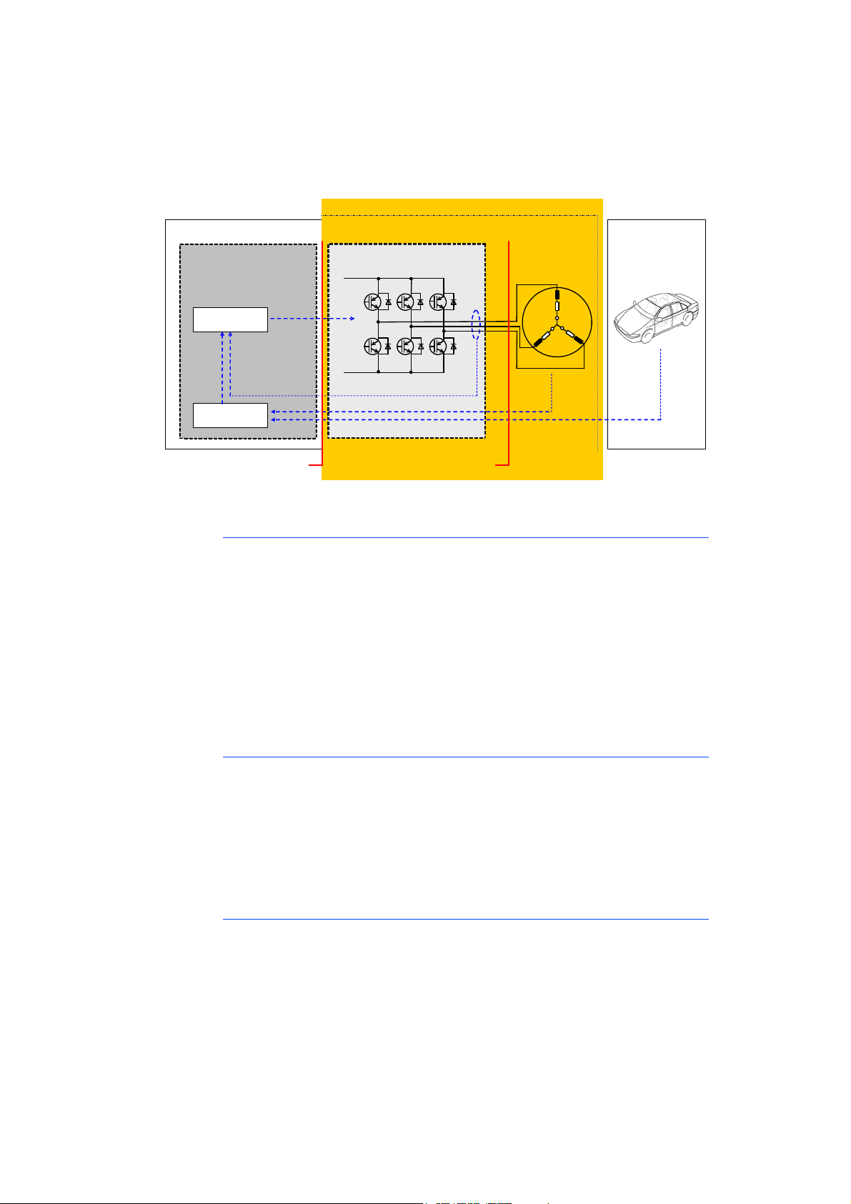
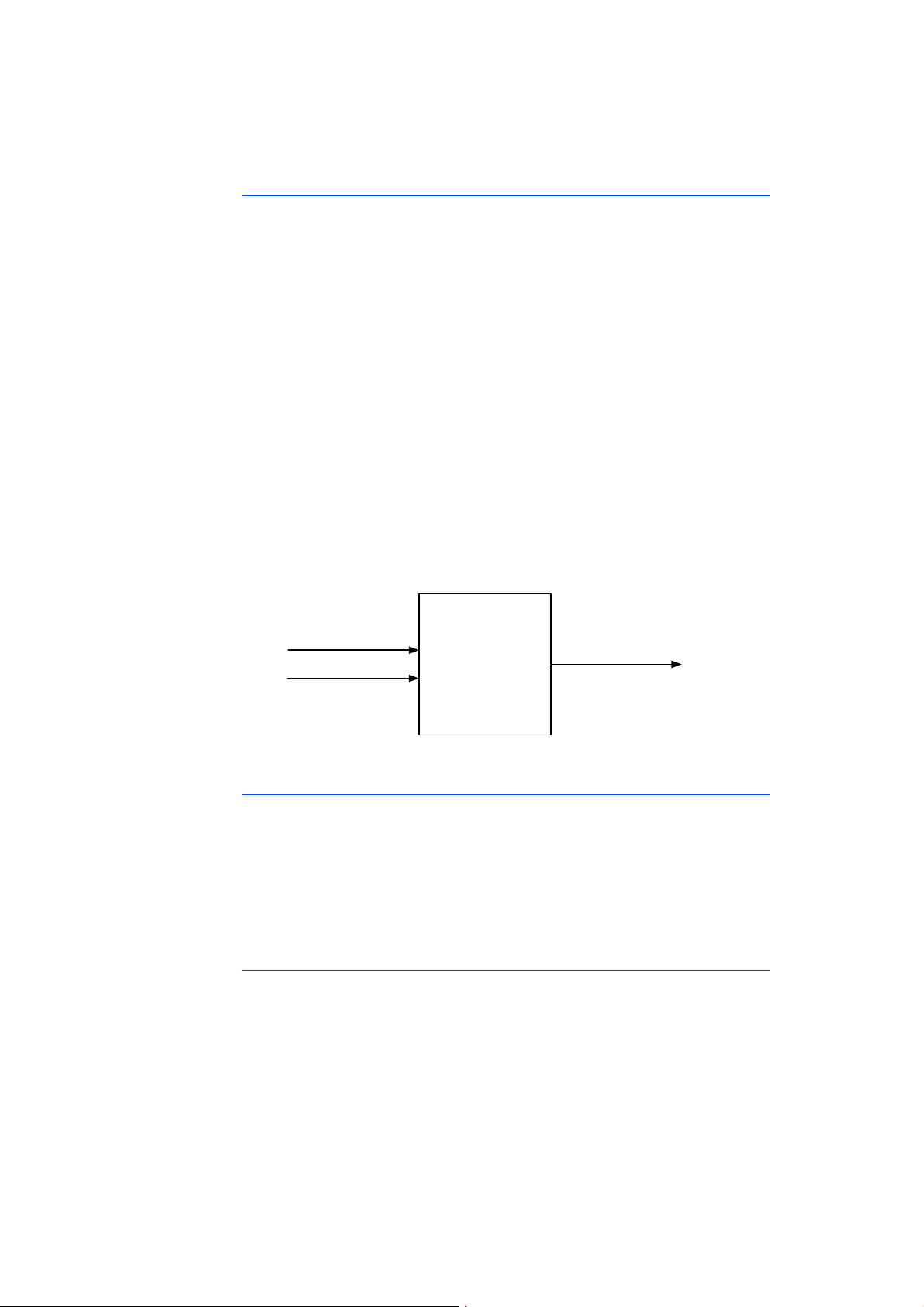
Fig. 1-1 below shows the components and interfaces of the complete "ECU - I/
O model (- DVE)" system.
Fig. 1-1 Components and interfaces of the ES5340.2
Parameterization of the Inverter
The inverter is configured using the typical variables, such as switching times,
polarity or resistances of the switches and diodes. In addition, for each switch,
the "open"/"closed" error states can be configured. Of course, what is known
as "free wheeling" (in which all 6 switches are open) can also be simulated.
In addition, for the entire inverter, the power loss of the ohmic components is
simulated – for the ohmic components, their value can also be calculated
depending on the temperature.
For the input wiring of the inverter, the internal resistance of the battery and the
capacity of the DC voltage link are taken into account – thus also allowing the
voltage in the DC voltage link to be simulated.
Parameterization of the PMSM
The PMSM is likewise configured via typical variables, such as the number of pole
pairs and cogging positions. Additional variables such as resistance, inductance,
the magnetic flow and the cogging torque can be changed during run time. This
ensures highly accurate simulation of the phase currents and electrical torque,
and all important variables can be changed in real time.
For the PMSM, the power loss of the ohmic components can also be simulated
and their temperature dependence can be calculated.
Parameterization the Connection to the Drive Train
For the mechanical connection to the drive train, the FPGA model also includes a
simulation of the spring-mass system. The system is configured with the typical
variables of coefficient of friction, moment of inertia for rotor and load, torsional
rigidity and damping. The load moment of the drive train can be preset and
changed during run-time.
ES5340.2 Electric Drive Simulation Board - User’s Guide8
Page 9
ETAS Introduction
6 x
PWM Gate Signal
VehiclePower Stage
phi_mech
omega_mech
load torque
PMSM
phi_elec
3 x
U_back_emf
P_loss
omega_elec
torque_elec
U_DC
3 x
U_phase
3 x
I_phase
6 x
U_switch
6 x
I_element
I_DC
U_Batt0
E-Motor
I_Batt0 I_DC
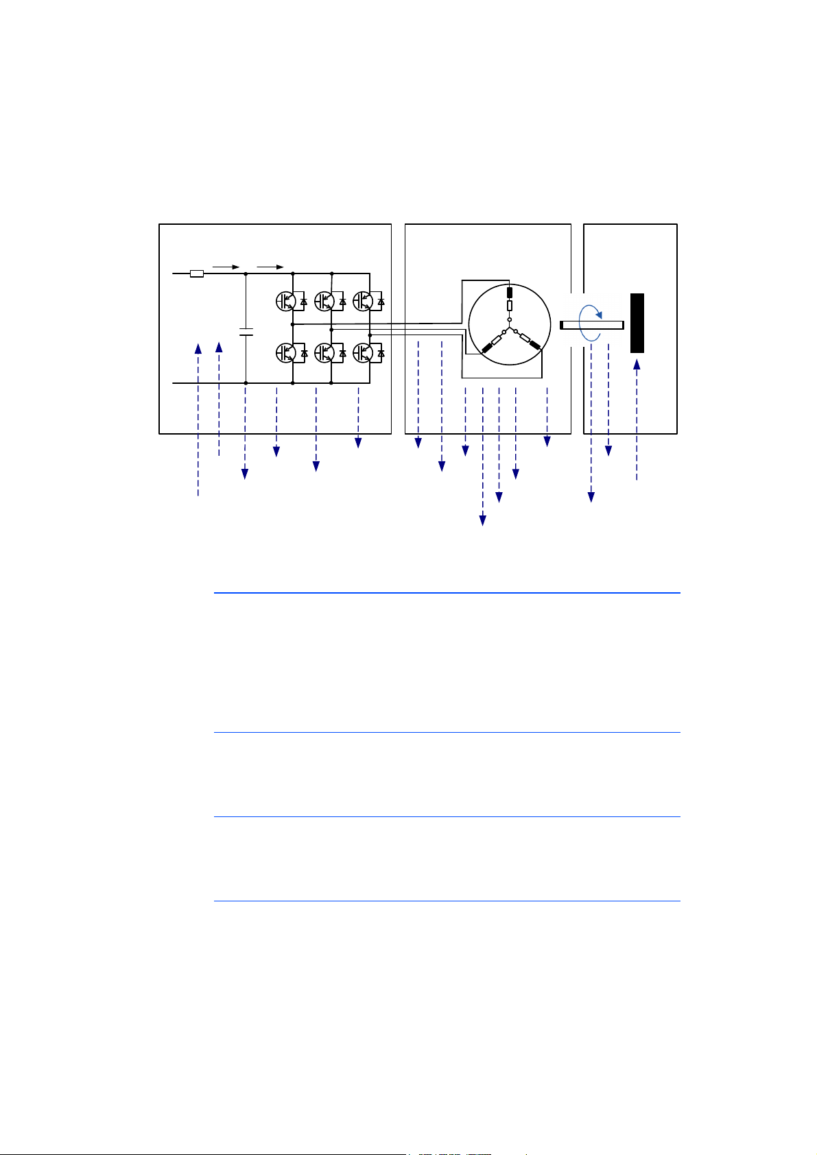
Fig. 1-2 shows the most important in- and output variables of the simulation
model. These variables can either be connected with another PC-based simulation model or output as electrical signals using the ES5340.2 Electric Drive Simulation Board or other hardware.
Fig. 1-2 Inputs and outputs of the FPGA model
1.1.3 Real-Time PC Model
Alternatively, a model of the electric motor can also be simulated on the RealTime PC. The ES5340.2 Electric Drive Simulation Board located in this RealTime PC (or connected to it via a PCI-Express expansion system) serves as an analog and digital I/O interface to the ECU.
Thus low latencies of between 5 μs and 10 μs are obtained for measurement of
the PWM control signals (for the inverter).
RPM Unit
The RPM unit present on the ES5340.2 can take over the position and speed of
the electric motor calculated by the model and then function as the RPM master
in the system.
Prediction of the Phase Currents
The current signals are output, supported by hardware, with an update rate of
1 MHz. By means of prediction, this takes place independently of the step size of
the Real-Time PC simulation model.
Clock Recovery for IGBT Control Signals
The synchronization for measuring the duty cycles and the control signals takes
place using an external synchronization signal or using clock recovery, i.e. the
automatic synchronization of center-aligned PWM control signals.
ES5340.2 Electric Drive Simulation Board - User’s Guide 9
Page 10

Introduction ETAS
1.1.4 Expansion with Slave Board
Using the ES5340.1-S slave board, 6 additional analog and 6 additional digital
outputs can be added (see "Versions of the ES5340.2 Electric Drive Simulation
Board" on page 10).
1.2 Versions of the ES5340.2 Electric Drive Simulation Board
The master board has the properties described below; the number of outputs
can be increased using an optional slave board (see "Electric Drive Simulation
Slave Board (ES5340.1-S)" on page 10).
1.2.1 Electric Drive Simulation Master Board (ES5340.2-M)
This board contains the full range of function:
I/O
• 8 analog outputs (incl. simulation of analog position sensor signals)
• 8 digital outputs (incl. simulation of digital position sensor signals)
• 20 digital inputs
• 4 analog inputs
Model Support
• FPGA model available
• RTPC model possible
1.2.2 Electric Drive Simulation Slave Board (ES5340.1-S)
This board has a reduced scope of function compared to the Master Board:
I/O
• 6 analog outputs (without simulation of analog position sensor signals)
• 6 digital outputs (without simulation of digital position sensor signals)
The source of each output signal is the values of the FPGA and RTPC model of a
ES5340.2-M.
ES5340.2 Electric Drive Simulation Board - User’s Guide10
Page 11
ETAS Introduction
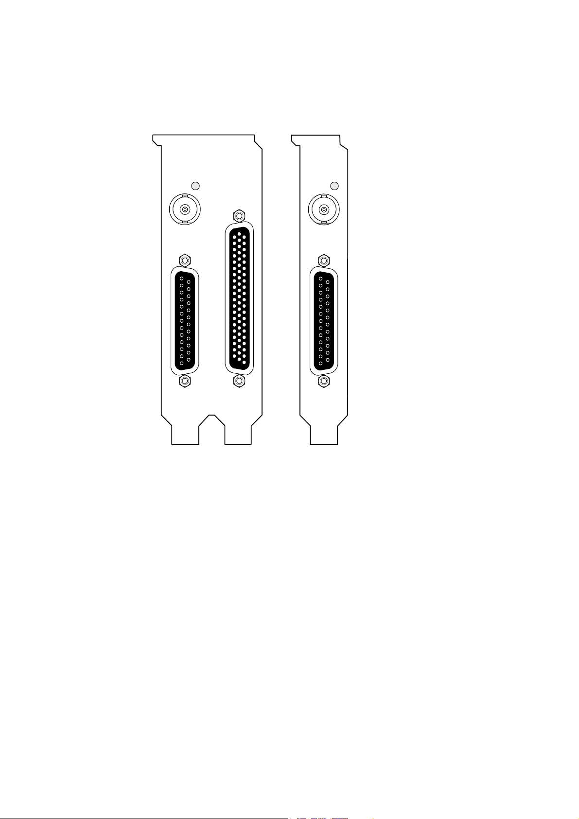
The following figure shows the front panel of the ES5340.2 Electric Drive Simulation Board with the various connections.
Fig. 1-3 Front panel of the ES5340.2 Electric Drive Simulation Board
(left: master, right: slave)
The function and assignment of the connectors are described in Chapter "Connector Assignment and Display Elements" on page 97.
ES5340.2 Electric Drive Simulation Board - User’s Guide 11
Page 12
Introduction ETAS
Analog Value 1...6
Analog Output CH0...CH5
Galvanic
Isolation
Analog Output
Multiplexer
Digital Value 1...6
Open Collector Output CH0...CH5
Galvanic
Isolation
Digital Output
Multiplexer
DSUB25
Analog Input Me asurement
Digital Input Mea surement
RPM Generator
Analog Postion Se nsors
Analog Output
Multiplexer
Analog Value 1. ..8
Digital Output
Multiplexer
SYNC Output
Analog Input CH0 …CH3
Analog Output CH0...CH5
Open Collector Output CH0...CH7
Galvanic
Isolation
Galvanic
Isolation
Galvanic
Isolation
Galvanic
Isolation
Galvanic
Isolation
FPGA Mode l (optional)
Digital Input CH00. ..CH19
Analog Output CH6...CH7
DSUB25
DSUB62HD
SENT Signals 1...4
Digital Value 1...8
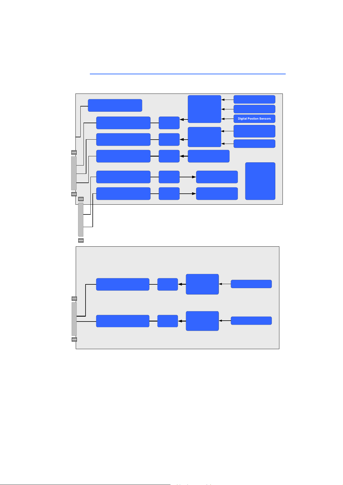
1.3 Block Diagram
Fig. 1-4 shows a block diagram with all important functional units of the
ES5340.2 Electric Drive Simulation Board.
Fig. 1-4 Block diagram of the ES5340.2 Electric Drive Simulation Board: Mas-
ter ES5340.2-M (top) and slave ES5340.1-S (bottom)
ES5340.2 Electric Drive Simulation Board - User’s Guide12
Page 13
ETAS Introduction
CAUTION!
WARNING!
DANGER!
Note
1.4 Basic Safety Instructions
Please adhere to the safety instructions in this manuals to avoid injury to yourself
and others as well as damage to the device.
1.4.1 Labeling of Safety Instructions
The safety instructions contained in this manual are shown with the standard
danger symbol shown below:
The following safety instructions are used. They provide extremely important
information. Please read this information carefully.
indicates a low-risk danger which could result in minor or less serious
injury or damage if not avoided.
indicates a possible medium-risk danger which could lead to serious
or even fatal injuries if not avoided.
indicates a high-risk, immediate danger which could lead to serious
or even fatal injuries if not avoided.
1.4.2 General Safety Information
Please read the product safety advice ("ETAS Safety Advice") as well as the following safety instructions to avoid injury to yourself and others as well as damage to the device.
Please read the documentation accompanying the product (this User’s Guide)
carefully before using the product.
ETAS GmbH cannot be made liable for damage which is caused by incorrect use
and handling and not adhering to the safety instructions.
1.4.3 Requirements for Users and Duties for Operators
The product may be assembled, operated and maintained only if you have the
necessary qualifications and experience for this product. Improper use or use by
a user without sufficient qualifications can put life at risk or cause damage to
health or property.
The system integrator is responsible for the safety of systems that use the product.
ES5340.2 Electric Drive Simulation Board - User’s Guide 13
Page 14

Introduction ETAS
General Safety at Work
Follow the existing regulations for work safety and accident prevention. All applicable regulations and statutes regarding operation must be strictly followed
when using this product.
1.4.4 Intended Use
Field of Application of the Product
The product is a PCI-Express plug-in board for the RTPC main board in the
ES5300.1-A Housing or for an RTPC by ETAS (TP_RTPC_2/3U.x). The product
must be used solely in the ES5300.1-A Housing or RTPC intended for this purpose.
The intended use of the product is as follows:
• Use as a component in industrial lab facilities or at industrial workplaces
• Use as a hardware interface for ECUs in a hardware-in-the-loop test system
• Use in conjunction with ETAS software that supports the ES5300.1-A
Housing and the ES5300.1-B Housing
• Use as an interface in conjunction with software programs that operate
the standardized, documented and open APIs from ETAS software products
The product is not intended for the following:
• Use within a vehicle on the road
• Use as part of a life support system
• Use as part of a medical application
• Applications in which misuse may result in injury or damage
• Use in environments in which conditions prevail that fall outside the specified ranges (see "Ambient Conditions" on page 113)
• Use with signal conditioning that falls outside the specified ranges (see
voltages, currents and power consumption in the section "Technical Data
and Standards" on page 111)
Requirements for the Technical State of the Product
The product is designed in accordance with state-of-the-art technology and recognized safety rules. The product must only be operated in a technically flawless
state, in accordance with its intended purpose and in a safety-conscious and hazard-aware manner under consideration of the documentation regarding the
product. If the product is not used in accordance with its intended purpose, its
product safety may be impaired.
Requirements for Operation
• Use the product only according to the specifications in the corresponding
user manual. If the product is used in any other way, product safety is no
longer ensured.
• Do not use the product in a wet or damp environment.
• Do not use the product in potentially explosive atmospheres.
ES5340.2 Electric Drive Simulation Board - User’s Guide14
Page 15
ETAS Introduction
WARNING!
WARNING!
Electrical Safety and Power Supply
Observe the regulations applicable at the operating location concerning electrical
safety as well as the laws and regulations concerning work safety!
Fire hazard!
Only use fuses that comply with the specification in the User's Guide
for the product. Never bridge defective fuses!
Failure to observe the fuse specification can lead to excess currents,
short circuits and fires.
Power Supply
The product is powered by the ES5300.1-A Housing or the ES5300.1-B Housing
via the PCIe slot on the main board of the RTPC.
Insulation Requirements for Lab Power Supplies to Circuits Connected to the HIL
System:
• The power supply to live circuitry must be safely isolated from the supply
voltage. For example, use a car battery or a suitable lab power supply.
• Only use lab power supplies with dual protection for the supply network
(with double/reinforced insulation (DI/RI)). This requirement is met by lab
power supplies that comply with IEC/EN 60950 or IEC/EN 61010.
• The lab power supply must be approved for use at a height of 2000 m and
in ambient temperatures of up to 40 °C.
De-Energizing a Plug-In Board
Switch off the ES5300.1-A Housing or the ES5300.1-B Housing and external
power supplies, and unplug the power cable and other plug connectors attached
to the plug-in board. Wait at least three minutes before removing the plug-in
board.
Approved Cables
The signal lines must not exceed a maximum length of 3 m.
Fire hazard!
Use only approved cables for creating cable assemblies (e.g. for connecting the ECU and external loads). The cables used must, in particular, be suitable for the currents, voltages and temperatures which
occur and must be flameretardant in accordance with one of the following standards IEC 60332-1-2, IEC 60332-2-2, UL 2556/
UL1581VW-1!
ES5340.2 Electric Drive Simulation Board - User’s Guide 15
Page 16
Introduction ETAS
WARNING!
CAUTION!
CAUTION!
CAUTION!
Requirements for the Installation Location
This is class A equipment. This equipment can cause radio interference in residential areas. Should that be the case, the operator may
be requested to institute reasonable measures.
Requirements for Ventilation
The air circulation inside the ES5300.1-A Housing and the ES5300.1B Housing can only be maintained if all free slots are covered with
front plates. Otherwise, it may lead to overtemperatures and trip the
overtemperature protection of the ES5300.1-A or the ES5300.1-B.
For this reason, install front plates in all free slots!
Transport and Installation
Some components of the product can be damaged or destroyed by
electrostatic discharges. Leave the plug-in board in its transport packaging until it is installed.
Only remove, configure and install the product at a workplace that is
protected against electrostatic discharges.
In order to prevent damage to the plug-in boards and the LABCAR
Housing, and thereby also avoid damage to property or health,
observe the installation instructions and information contained in the
relevant User's Guides.
Connecting/Disconnecting Devices
To avoid injuries and hardware damages, please observe the following precautionary measures:
• Do not apply any voltages to the connections of the product that do not
correspond to the specifications of the respective connection.
• Do not connect or disconnect any devices while the ES5300.1-A Housing,
the ES5300.1-B Housing or connected devices are switched on. First,
switch off the ES5300.1-A Housing and the ES5300.1-B Housing by shutting down the real-time PC and by pressing the On/Off switch at the rear,
then unplug the power cable.
• When plugging in connectors, ensure that they are inserted straight and
no pins are bent.
ES5340.2 Electric Drive Simulation Board - User’s Guide16
Page 17

ETAS Introduction
Maintenance
The product does not require maintenance.
Repairs
If an ETAS hardware product needs to be repaired, return the product to ETAS.
Cleaning
The product is not expected to require cleaning.
ES5340.2 Electric Drive Simulation Board - User’s Guide 17
Page 18
Introduction ETAS
1.5 Identifications on the Product
The following symbols are used for identifying the product:
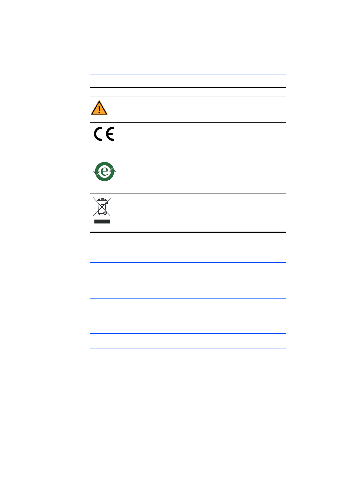
Symbol Description
The User's Guide must be read prior to the startup of the
product
Identification for CE conformity (see "CE Marking"
on page 18)
Identification for China RoHS (see "RoHS Conformity"
on page 18)
Identification for WEEE directive
(see "Taking the Product Back and Recycling" on page 19)
Observe the information in the chapter "Technical Data and Standards"
on page 111.
1.5.1 CE Marking
ETAS confirms that the product meets the product-specific applicable European
Directives with the CE marking affixed to the product or its packaging. The CE
Declaration of Conformity for the product is available upon request.
1.5.2 KC Mark
With the KC mark attached to the product and its packaging, ETAS confirms that
the product has been registered in accordance with the product-specific KCC
guidelines of the Republic of Korea.
1.5.3 RoHS Conformity
European Union
The EU Directive RoHS 2011/65/EU limits the use of certain dangerous materials
for electrical and electronic devices (RoHS conformity).
ETAS confirms that the product corresponds to this directive which is applicable
in the European Union.
China
ETAS confirms that the product meets the product-specific applicable guidelines
of the China RoHS (Management Methods for Controlling Pollution Caused by
Electronic Information Products Regulation) applicable in China with the China
RoHS marking affixed to the product or its packaging.
ES5340.2 Electric Drive Simulation Board - User’s Guide18
Page 19
ETAS Introduction
1.6 Taking the Product Back and Recycling
The European Union has passed a directive called Waste Electrical and Electronic
Equipment, or WEEE for short, to ensure that systems are set up throughout the
EU for the collection, treatment and recycling of electronic waste.
This ensures that the devices are recycled in a resource-saving way representing
no danger to health or the environment.
Fig. 1-5 WEEE Symbol
The WEEE symbol on the product or its packaging shows that the product must
not be disposed of as residual garbage.
The user is obliged to collect the old devices separately and return them to the
WEEE take-back system for recycling.
The WEEE Directive concerns all ETAS devices but not external cables or batteries.
For more information on the ETAS GmbH Recycling Program, contact the ETAS
sales and service locations (see "ETAS Contact Addresses" on page 115).
1.7 Materials Subject to Declaration
Some products from ETAS GmbH (e.g. modules, boards, cables) use components
with materials that are subject to declaration in accordance with the REACH regulation (EC) no.1907/2006. Detailed information is located in the ETAS download center in the customer information "REACH Declaration" <www.etas.com/
Reach>. This information is continuously being updated.
ES5340.2 Electric Drive Simulation Board - User’s Guide 19
Page 20

Introduction ETAS
1.8 About This Manual
This manual consists of the following chapters:
• "Introduction" on page 7
This chapter
• "Installation and Configuration" on page 23
• "Hardware Description" on page 31
• "FPGA Models" on page 49
• "Configuring the Hardware in LABCAR-RTC" on page 65
• "Connector Assignment and Display Elements" on page 97
• "Order Information and Scope of Delivery" on page 103
• "Technical Data and Standards" on page 111
• "ETAS Contact Addresses" on page 115
1.8.1 Using This Manual
Representation of Information
All activities to be carried out by the user are shown in what we call a "UseCase" format, i.e. the target to be achieved is defined briefly in the title and the
individual steps necessary to achieve this target are then listed. The information
is displayed as follows:
Target definition
Any introductory information...
1. Step 1
Possibly an explanation of step 1...
2. Step 2
Possibly an explanation of step 2...
Any concluding remarks...
Concrete example:
To create a new file
If you want to create a new file, no other file may be open.
1. Select File → New.
The "Create file" dialog box appears.
2. Enter a name for the file in the "File name" field.
The file name must not exceed 8 characters.
3. Click OK.
The new file is created and saved under the name specified. You can now work
with the file.
ES5340.2 Electric Drive Simulation Board - User’s Guide20
Page 21

ETAS Introduction
Note
Typographic Conventions
The following typographic conventions are used:
Select File → Open. Menu commands are shown in boldface/
blue.
Click OK. Buttons are shown in boldface/blue.
Press <ENTER>. Keyboard commands are shown in angled
brackets in block capitals.
The "Open File" dialog box
appears.
Select the file setup.exe. Text in drop-down lists, program code, as
A conversion between the file types
logical and arithmetic is not possible.
Names of program windows, dialog boxes,
fields etc. are shown in quotation marks.
well as path and file names are shown in
the Courier font.
Content markings and newly introduced
terms are shown in italics.
Important notes for the user are shown as follows:
Important note for the user.
ES5340.2 Electric Drive Simulation Board - User’s Guide 21
Page 22

Introduction ETAS
ES5340.2 Electric Drive Simulation Board - User’s Guide22
Page 23

ETAS Installation and Configuration
2 Installation and Configuration
This chapter contains important information on the following topics:
• "Installing the ES5340.2 in the Real-Time PC" on page 24
If you are setting up your Real-Time PC yourself or installing the PCIExpress board in an existing Real-Time PC at a later date, make sure you
carefully follow the tips and instructions contained in this chapter.
• "Master/Slave Configuration" on page 25
To extend the I/O capacity of the ES5340.2-M (master), a slave card
(ES5340.1-S) can be installed. This makes it possible to increase the number of analog and digital outputs by six each.
• "RPM Master/Slave Configuration" on page 26
The RPM unit on the ES5340.2 can be operated as a master or slave.
• "“Exclusive Core Usage” Mode" on page 28
When the phase currents and voltages in a software model (on the RealTime PC) are simulated according to the PWM signals of the inverter controller, the model has to be calculated in a task < 50 μs.
ES5340.2 Electric Drive Simulation Board - User’s Guide 23
Page 24
Installation and Configuration ETAS
Note
Note
CAUTION!
2.1 Installing the ES5340.2 in the Real-Time PC
If you are setting up your Real-Time PC yourself or installing the PCI-Express
board in an existing Real-Time PC at a later date, make sure you carefully follow
the tips and instructions contained in this chapter.
2.1.1 Requirements and Specifications
Released PCs and Known Installations
A list with PCs tested and released by ETAS as well as known installations (LABCAR-RTPC Vx.y.z HW Compatibility List.pdf) can be found in the
Web Interface of LABCAR-RTPC at Main Page → Documentation.
Because the booting time of the ES5340.2 is more than 800 μs, PCs not
released by ETAS may not detect the card!
When using the ES5340.2, the hardware of the Real-Time PC should fulfill the
following requirements - in addition to the hardware specifications described in
the "LABCAR-RTPC User's Guide":
Southbridge Chip ICH 2, 4, 5, 6, 7, 8, 9 e.g. Intel chipsets 915, 925,
PCIe slots Min. 1 (x4 or more)
Tab. 2-1 Additional Requirements for the Real-Time PC
To guarantee the necessary performance when using several PCI-Express
boards, the power supply should have a minimum performance of 400 W.
2.1.2 Installation
Please observe the following when installing an ES5340.2 Electric Drive Simulation Board:
• Before installation, power off your Real-Time PC and disconnect it from
the mains.
• Please take the following precautionary measures to avoid hardware
being damaged by static discharge:
945, 955, 965, 975, E7230 and
X38, X48, X58
Some components of the ES5340.2 Electric Drive Simulation Board
may be damaged or even destroyed by static discharge. Leave the
board in its transport package until you want to install it.
The ES5340.2 Electric Drive Simulation Board should only be taken
from its package, configured and installed at a working place that is
protected against static discharge.
• Follow the instructions of the PC manufacturer on how to install expansion boards
ES5340.2 Electric Drive Simulation Board - User’s Guide24
Page 25
ETAS Installation and Configuration
2.2 Master/Slave Configuration
To extend the I/O capacity of the ES5340.2-M (master), a slave card (ES5340.1S) can be installed. This makes it possible to increase the number of analog and
digital outputs by six each.
For this purpose, you have to decide whether you are going to work with an
FPGA model or a model on the Real-Time PC.
Using an FPGA Model on the Master
By connecting the master and slave card of what is referred to as a Gigabit Link,
all the slave card outputs can be addressed by the FPGA model with the typically
low latencies (< 1 μs) (see "Connecting Master and Slave via Gigabit Link"
on page 25).
Using a Model on the Real-Time PC
In this case, the ES5340.1-S can simply be inserted into a PCI-Express slot – once
configured in LABCAR-RTC, the outputs of the ES5340.1-S can be addressed via
the LABCAR-OPERATOR Connection Manager.
2.2.1 Connecting Master and Slave via Gigabit Link
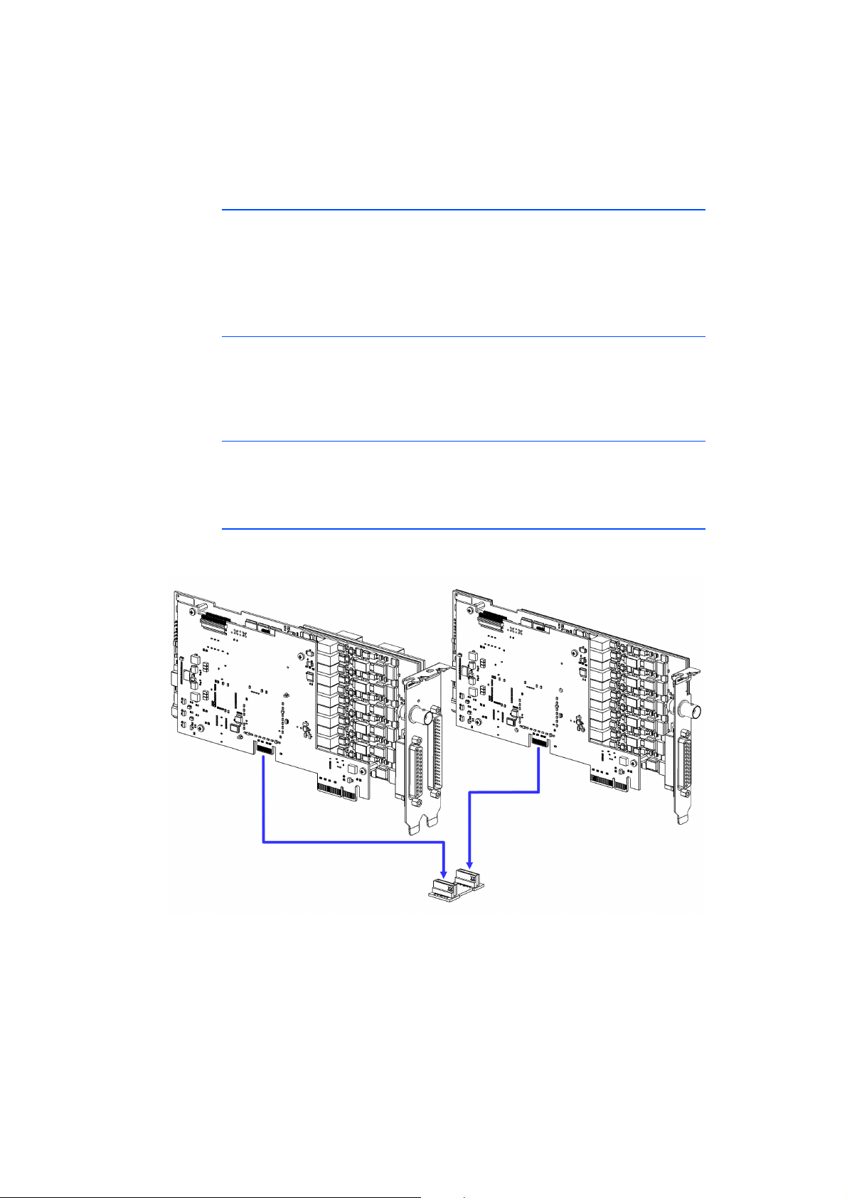
The following figure shows the connection of an ES5340.2-M with an ES5340.1S via Gigabit Link.
The bridge for the Gigabit Link is a small board with two connectors supplied
with an ES5340.1-S. The slave card has to be installed to the right of the master.
First connect master and slave with the bridge (see figure) and then insert them
into two neighboring PCI-Express slots.
ES5340.2 Electric Drive Simulation Board - User’s Guide 25
Page 26
Installation and Configuration ETAS
Note
2.2.2 Configuration in LABCAR-RTC
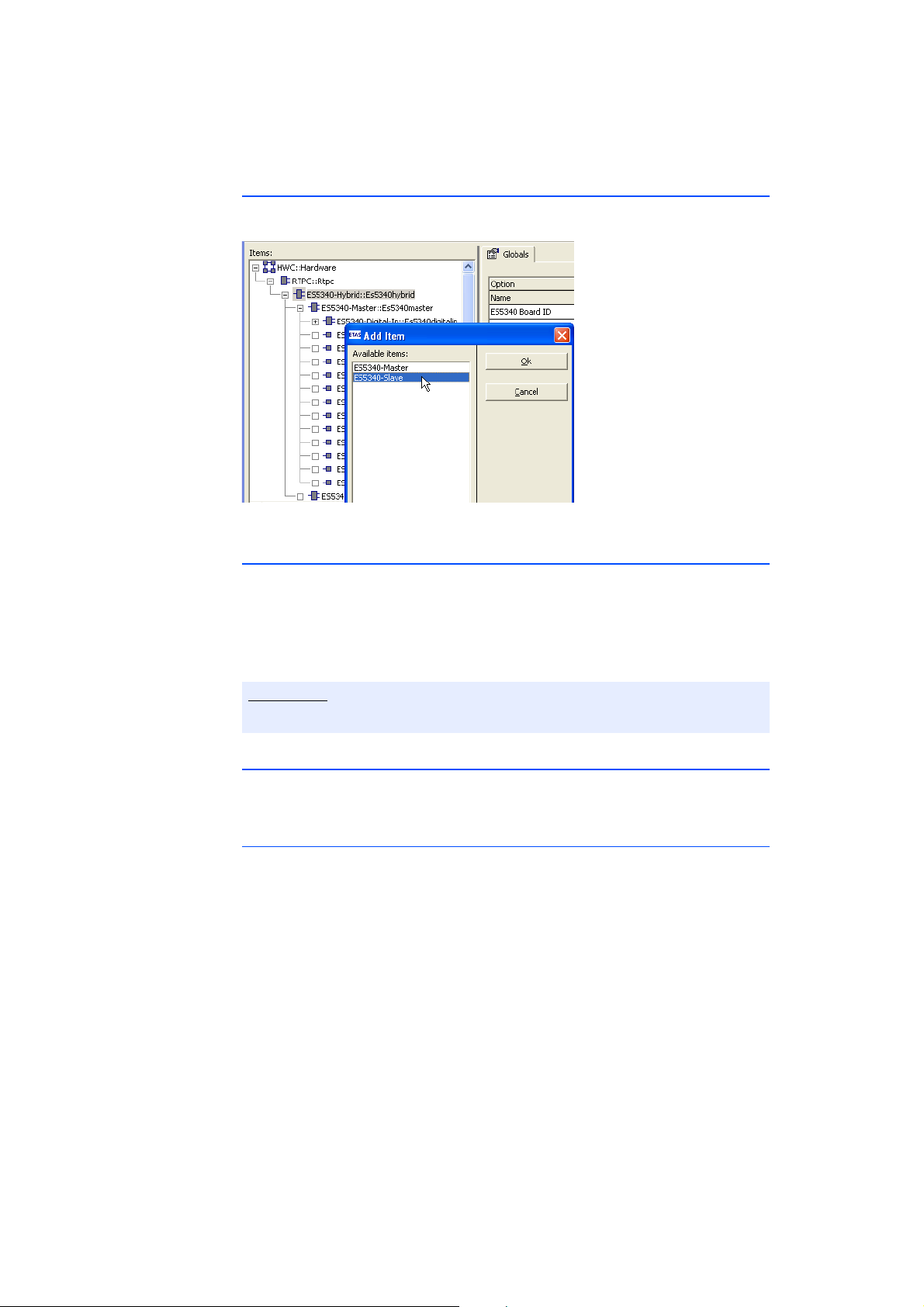
To configure the slave card in LABCAR-RTC, you have to incorporate an
“ES5340-Slave” subsystem.
You can then configure the additional outputs to suit your requirements.
2.3 RPM Master/Slave Configuration
The RPM unit on the ES5340.2 can be operated as a master or slave.
The RPM unit can also assume the position and speed of the e-engine calculated
by the model and then act as RPM master in the system. For this purpose, the
RPM buses of the master and of one or more of the slaves have to be connected
as described below.
The following only applies to boards in PCI-Express slots!
2.3.1 Connecting the RPM Buses of Two Boards
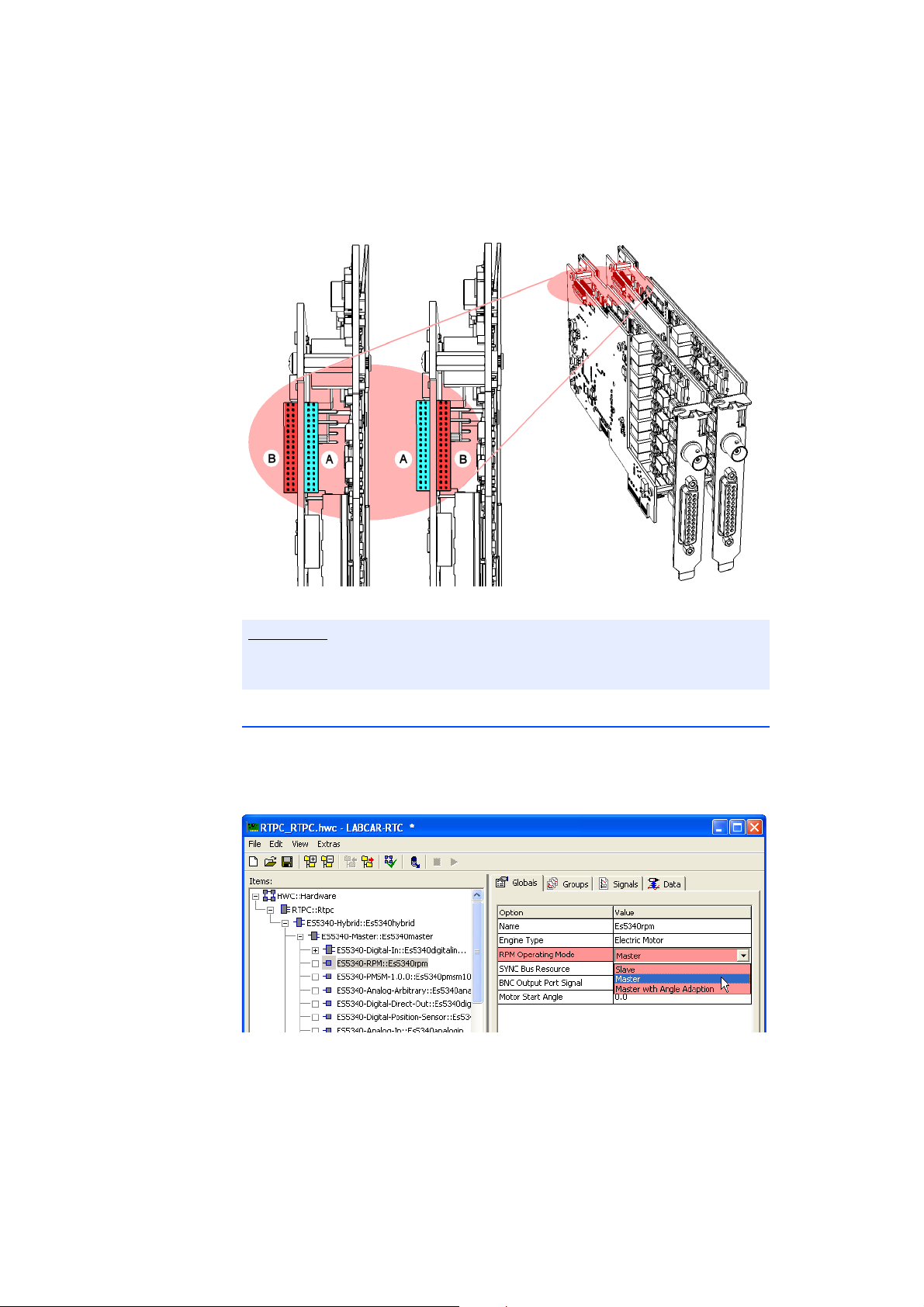
There are two connectors on each board for connecting the RPM signal. These
are connected with an appropriate cable.
Installation
• When installing a further board or connecting two existing boards for a
master/slave configuration, first power off your Real-Time PC.
• Observe the points described in "Installation" on page 24.
• Connect the neighboring connectors of two boards (connectors A in
Fig. 2-1) with one of the ribbon cables provided.
ES5340.2 Electric Drive Simulation Board - User’s Guide26
Page 27
ETAS Installation and Configuration
Note
• Terminate the opposing connections (connectors B in Fig. 2-1 ) with the
terminating connectors provided.
An individual board must be terminated with one terminating connector.
Fig. 2-1 Connecting the RPM buses of two boards
Before carefully pushing the connectors into the sockets, make sure that the
pins are lined up correctly with the socket!
2.3.2 Configuration of the RPM Unit (in LABCAR-RTC)
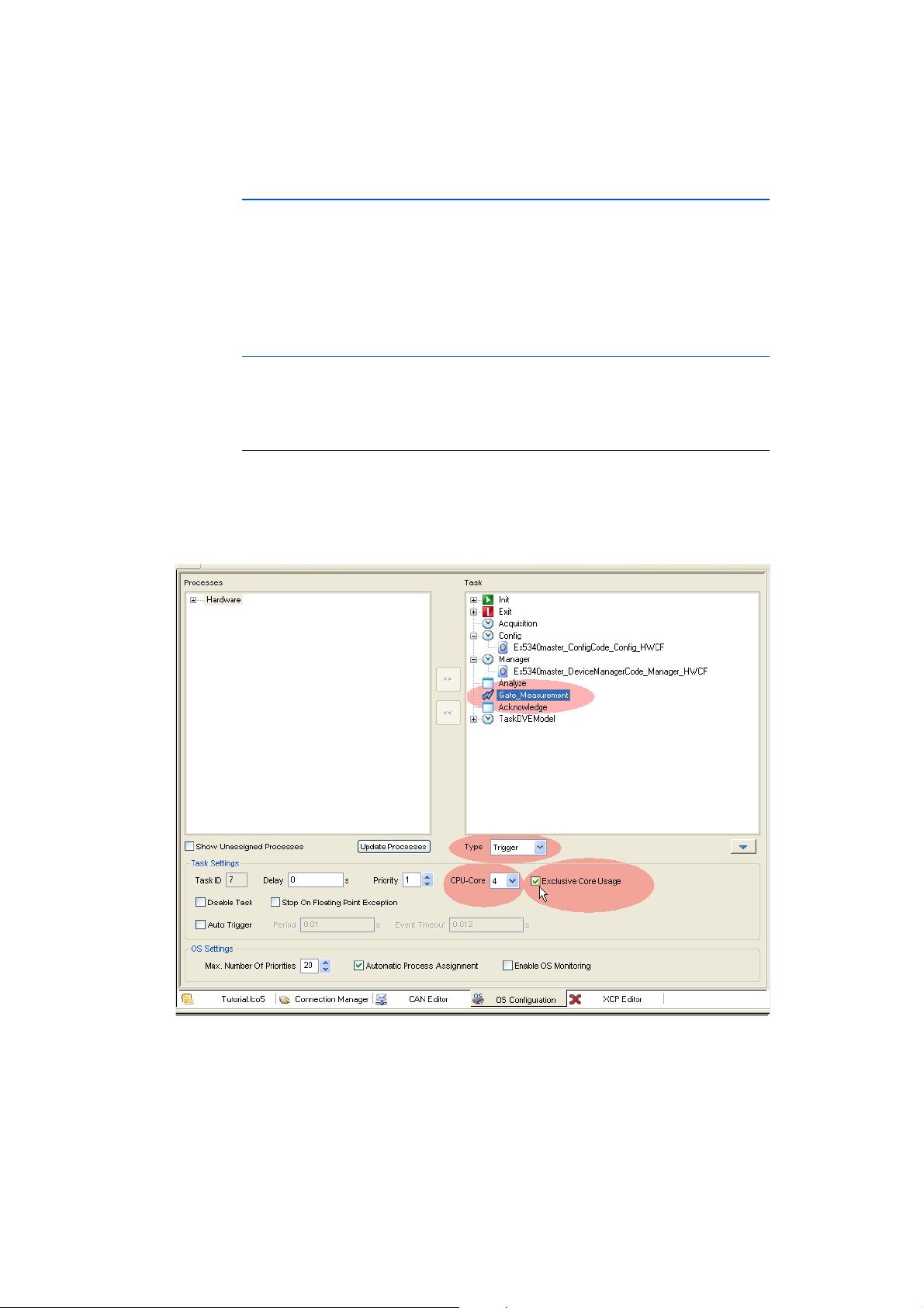
The allocation of whether an RPM unit is to act as a master or slave, is defined in
the relevant “ES5340-RPM” item. In the “Globals” tab, you can set the “RPM
Operating Mode” option accordingly (see "Configuring the RPM unit in LABCAR-RTC" on page 48).
ES5340.2 Electric Drive Simulation Board - User’s Guide 27
Page 28
Installation and Configuration ETAS
2.4 “Exclusive Core Usage” Mode
When the phase currents and voltages in a software model (on the Real-Time PC)
are simulated according to the PWM signals of the inverter controller, the model
has to be calculated in a task < 50 μs.
This can be done by directly accessing a dedicated processor core (“Exclusive
Core Usage”). This means that between the control signals being output and the
current signals being measured there are no raster losses in the ECU.
Prerequisites
To use this mode the processor of the Realtime PC must have at least four cores
and at least one of these cores must not be being used by another task (see
below).
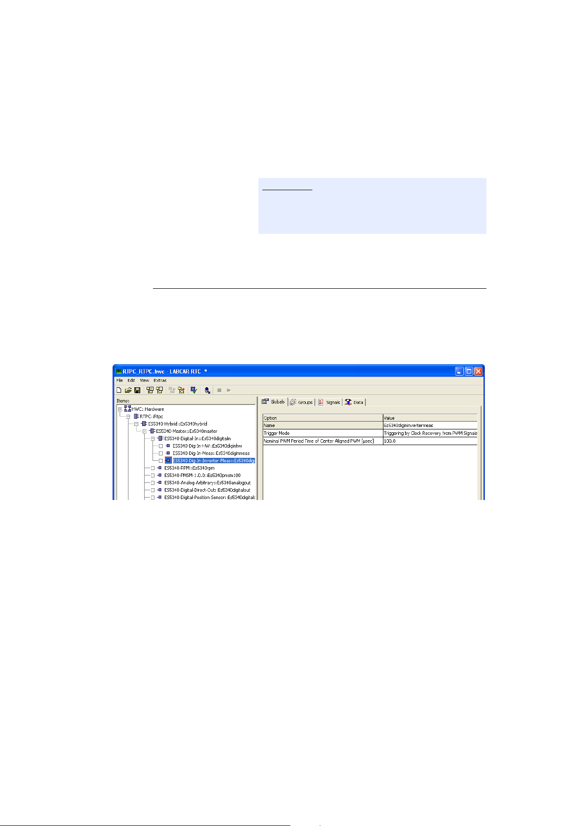
To create a task for “Exclusive Core Usage”
1. Toggle to the “OS Configuration” tab in LABCARIP.
2. Create a new task (Add Task in the shortcut menu)
in the “Task” box.
Rename the task (Rename).
3. Select “Trigger” as “Type”.
4. Select the option “Exclusive Core Usage”.
ES5340.2 Electric Drive Simulation Board - User’s Guide28
Page 29
ETAS Installation and Configuration
Note
5. For “CPU Core”, select the core that is to be available exclusively for this task.
Only cores not used by another task are displayed
here – you may have to release a core (by reconfiguring other tasks).
The total number of existing processor cores is not
known in LABCAR-IP – only assign cores that are
actually available!
6. Save the project.
To configure measuring in LABCAR-RTC
1. Open the hardware configuration in LABCAR-RTC.
2. Select the item “ES5340-Dig-In-Inverter-Meas”.
3. In the “Globals” tab, select the required settings for
the options “Trigger Mode” and “Nominal PWM
Period Time of Center-Aligned PWM [μsec]”.
4. Toggle to the “Groups” tab.
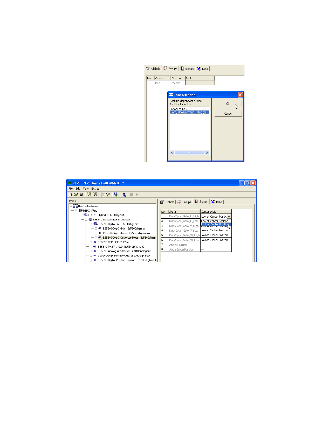
5. Click the table field in the “Task” column.
6. The “Task selection” window opens.
All “Trigger” tasks for which “Exclusive Core
Usage” has been activated and which are defined in
the OS Configuration of LABCAR-IP are listed here.
ES5340.2 Electric Drive Simulation Board - User’s Guide 29
Page 30
Installation and Configuration ETAS
7. Select the required task and click Ok.
8. Set the polarity of the gate signals in the “Signals”
tab (“Center Logic” column).
9. Save the settings (File → Save).
ES5340.2 Electric Drive Simulation Board - User’s Guide30
Page 31
ETAS Hardware Description
Note
3 Hardware Description
This chapter provides a description of the inputs and outputs of the ES5340.2
Electric Drive Simulation Board along with the signals that it can measure and
those that can be generated for it.
The step-by-step execution of the configuration is in the chapter "Configuring
the Hardware in LABCAR-RTC" on page 65.
Specifically, it includes information about the following topics:
• "Generating Analog Signals" on page 32
These outputs are used for different analog signals via an output multiplexer.
– "Specification" on page 32
– "Configuring the Analog Signals" on page 33
• "Output Multiplexers for the Analog Signals" on page 36
Each analog output has a multiplexer that can be used to define the signal
for this output.
• "Generating Digital Signals" on page 38
These outputs are used for different digital signals via an output multiplexer.
– "Specification" on page 38
– "Configuring the Digital Signals" on page 40
• "Output Multiplexers for the Digital Signals" on page 41
Each digital output has a multiplexer that can be used to define the signal
for this output.
• "Analog Inputs" on page 42
The ES5340.2-M has four inputs for measuring analog signals.
– "Specification" on page 42
– "Configuring the Analog Inputs" on page 42
• "Digital Inputs" on page 42
The ES5340.2-M has 20 inputs for measuring digital signals.
– "Specification" on page 42
– "Configuring the Digital Inputs" on page 43
• "RPM Generator" on page 47
The ES5340.2 Electric Drive Simulation Board has a central RPM Generator
that outputs a speed-specific clock signal.
– "Angle Clock Signal" on page 47
– "Synchronization" on page 48
– ""Master with Angle Adaptation" RPM Mode" on page 48
ES5340.2 Electric Drive Simulation Board -User’s Guide 31
Page 32
Hardware Description ETAS
REF
IN
OUT = IN x REF
OUT
FPGA
External
Reference
Galv. Iso.
10 V Ref
Galv. Iso.
DAC
ECU
ADC
Sensor Supply
Voltage
3.1 Generating Analog Signals
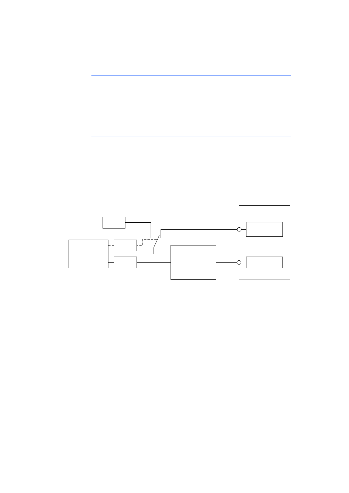
These outputs are used for different analog signals via an output multiplexer.
The ES5340.2-M has eight analog outputs, two of which are dedicated to
simulating the analog speed sensor/resolver. The other six analog outputs can be
used to simulate additional analog speed sensors or to output analog signals.
The ES5340.1-S has six analog outputs (no simulation of speed sensors possible).
3.1.1 Specification
The output voltage range is -10 V to +10 V for internal reference or -12 V to
+12 V for external reference voltage – the resolution of the D/A converter is
16 bits.
All outputs are electrically insulated and have an electric strength of ±60 V.
In addition, each output has a cutoff relay.
The accuracy (internal reference) is ±5 mV, while the maximum current of an
output is ±30 mA.
The following illustration shows the schematic circuit diagram of an output.
Fig. 3-1 Schematic circuit diagram of the analog outputs
For each of the six channels CH0 to CH5, you can choose between the internal
(10 V) and the external source for the reference voltage (in LABCAR-RTC:
"ES5340-Analog-Out-Mux" device, "Signals" tab, "Reference Voltage"
column).
Only the same external reference can be assigned to the two channels reserved
for the simulation of the analog resolver speed sensor, CH6 and CH7. In this
case, the external reference can be connected to two pins: one for GND and one
for the signal of the external reference (see "Assignment of the connectors for
the inputs" on page 100) .
ES5340.2 Electric Drive Simulation Board -User’s Guide32
Page 33
ETAS Hardware Description
3.1.2 Configuring the Analog Signals
Which signals are assigned to the eight (ES5340.2-M) or six (ES5340.1-S) outputs
is defined in the output multiplexer (see "Output Multiplexers for the Analog
Signals" on page 36).
You can configure the analog channels themselves as follows.
Analog Direct Out
This can be used to output constant voltages and values calculated in the computation grid of an RTPC model – specified by the value of "OutValue_n" [-1.0
to +1.0]:
U
= OutValue n * U
out
Ref
Resolver
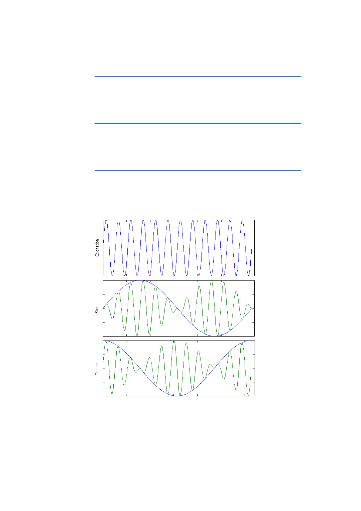
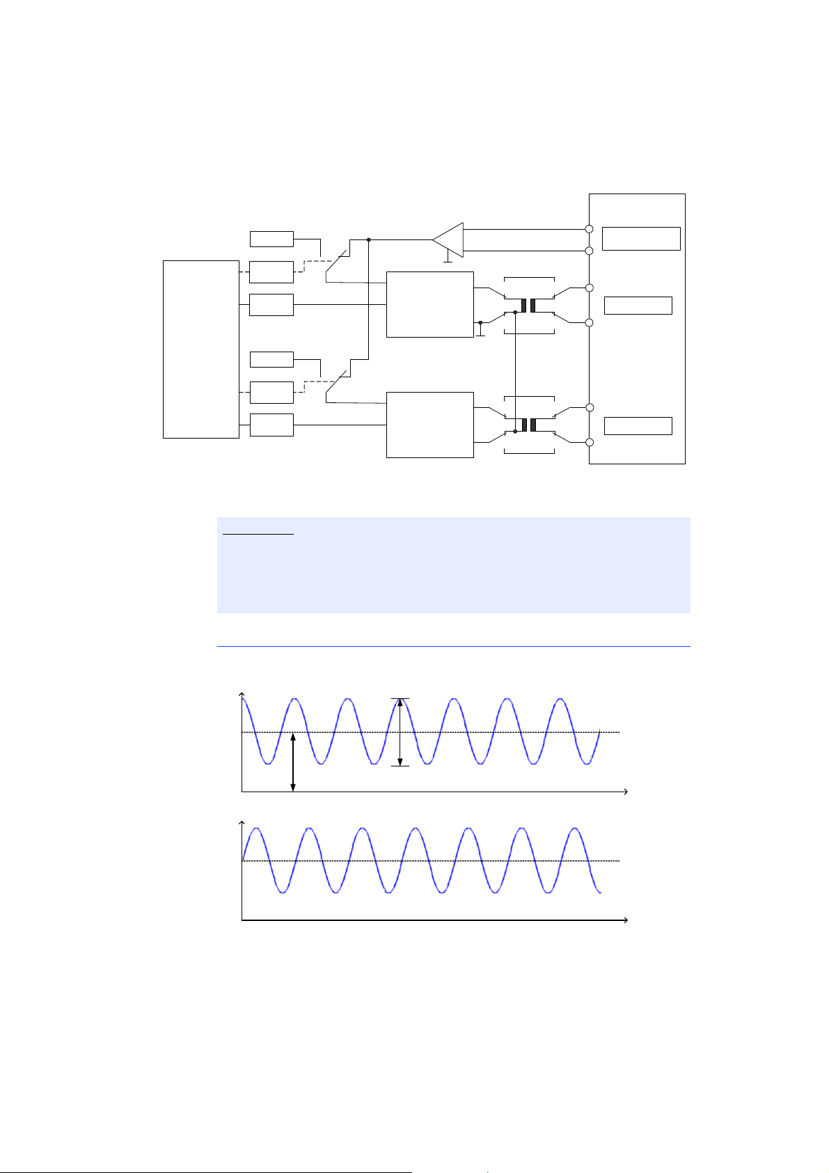
If a resolver is used as the speed sensor, two analog channels (CH6 and CH7) can
be used for the output of the sine and cosine signal (see Fig. 3-2).
The following sensor chips have been tested:
• R/D Converter AD2S1210 (Analog Devices)
•Smartcoder
®
AU6802N1 (Tamagawa Seiki)
Fig. 3-2 Signals for the resolver
ES5340.2 Electric Drive Simulation Board -User’s Guide 33
Page 34
Hardware Description ETAS
Note
REF
IN
Out = IN x REF
OUT
FPGA
Excitation
Galv. Iso.
Sin
10 V Ref
Galv. Iso.
DAC
ECU
ADC
Excitation Signal
Generation
REF
IN
OUT = IN x REF
OUT
Internal
Reference
Galv. Iso.
10 V Ref
Galv. Iso.
DAC
ECU
ADC
Cos
+
-
A
B
2.5 V
1 V
t
t
The excitation signal is connected instead of an external reference (see Fig. 3-3
and "Assignment of the connectors for the inputs" on page 100).
Fig. 3-3 Schematic circuit diagram of an analog output configured as
"resolver"
When using a resolver as position sensor, AGND of channel 6 (pin 43 and 44 of
the DSUB62HD connector) has to be connected with AGND of
channel 7 (pin 45 and 46 of the DSUB62HD connector)!
Without this connection the ES5340.2 cannot detect the excitation signal!
Sine Encoder
If a sine encoder (Vogt sensor) is used as the speed sensor, any two analog channels can be used for the A and B signals (see Fig. 3-4).
Fig. 3-4 Signals A and B of the sine encoder
ES5340.2 Electric Drive Simulation Board -User’s Guide34
Page 35
ETAS Hardware Description
Update of sensor values every dT Continuous update of sensor values
Sine Extrapolated
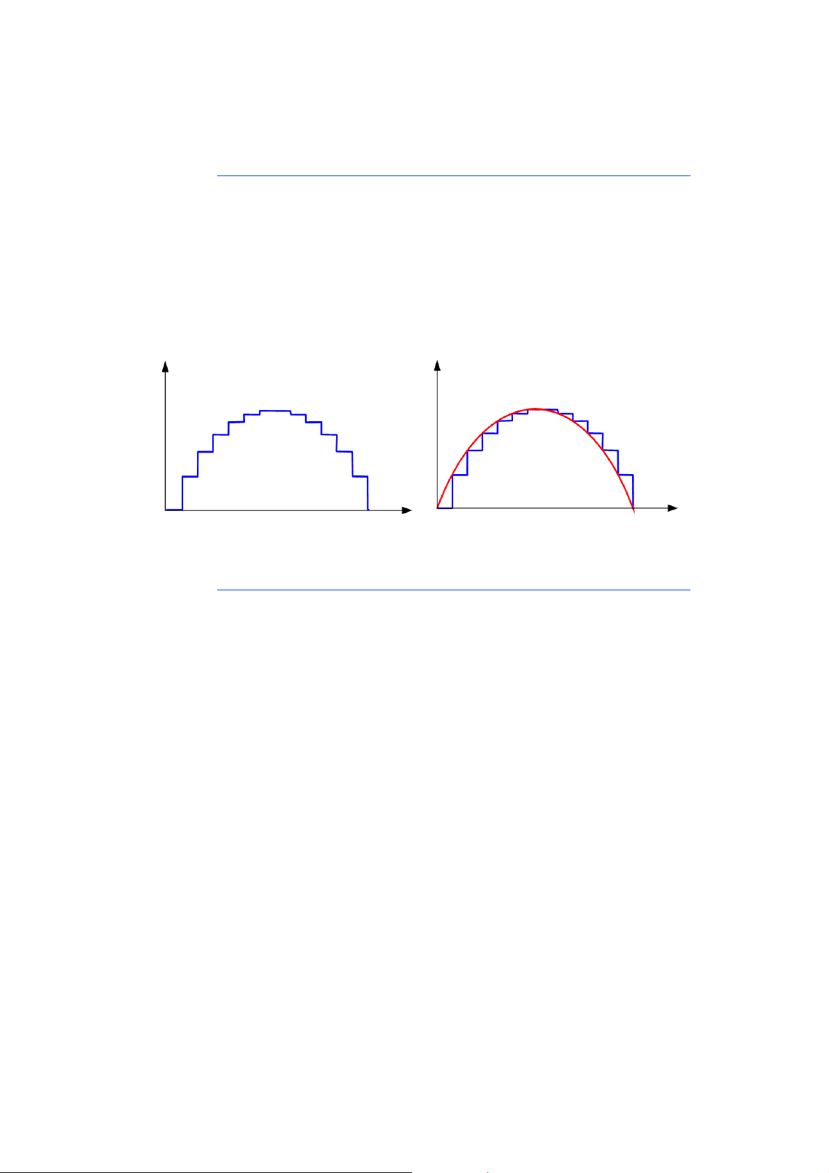
If a model that runs on the Real-Time PC is used for the simulation, it can be used
to generate sinusoidal signals such as phase currents I
, Iv ,Iw.
u
With each computing cycle, the Real-Time PC model calculates an amplitude
value for each phase current and phase voltage and a phase for these. With
these values, the phase currents or phase voltages are output, independently of
the computing cycle of the PC-based model, with an update rate of 1 μs.
The advantage of this is that the output signals are not step functions (with the
step size of the PC-based model), but rather are output continuously, so to
speak.
The signal generators are controlled by the central RPM unit, which runs at the
mechanical angular velocity.
Analog Arbitrary
Here, preset "waveform tables" are output – the following can be configured:
• The amplitude value
• A voltage offset
•A phase
• The value for a phase change speed
Outputs for arbitrary signals can be used to output user-defined signal patterns
(based on the current angle of the simulated electric motor).
This signal pattern can be used, for example, to simulate specific position sensors
and other variables with a direct relationship to the motor angle.
ES5340.2 Electric Drive Simulation Board -User’s Guide 35
Page 36

Hardware Description ETAS
Note
3.2 Output Multiplexers for the Analog Signals
Each analog output has a multiplexer that can be used to define the signal for
this output.
Sources for the Analog Outputs
The analog output channels can be driven by two different sources:
• Outputs of the FPGA model
• Signals of type "Analog Direct Out" and analog arbitrary signals (incl.
position sensors such as resolvers and sine encoders)
The sources are configured in LABCAR-RTC with the "ES5340-Analog-Out-Mux"
item, "Signals" tab in the "Output Select" column.
For a ES5340.2-M, eight signals can be configured for the outputs here; for a
ES5340.1-S, an additional six can be configured.
For slave cards (ES5340.1-S), only "Analog Direct Out" can be selected.
ES5340.2 Electric Drive Simulation Board -User’s Guide36
Page 37

ETAS Hardware Description
When using an FPGA model, the following signals are available as multiplexer
inputs:
Signal Component Meaning
U_DC Inverter Inverter voltage
U_Phase_X
(X = U,V,W)
U_d Inverter Voltage in d direction
U_q Inverter Voltage in q direction
U_switch_XH
(X = U,V,W)
U_switch_XL
(X = U,V,W)
I_element_XH
(X = U,V,W)
I_element_XL
(X = U,V,W)
I_DC Inverter Inverter current
U_back_EMF_X
(X = U,V,W)
I_d PMSM* Voltage in d direction
I_q PMSM* Voltage in q direction
I_Phase_X
(X = U,V,W)
T_el PMSM* Torque of electric motor
Omega_mech Mechanical system Angular velocity: rotor
Phi_mech Mechanical system Angle: rotor
Omega_el Mechanical system Angular velocity: electrical field
Phi_el Mechanical system Angle: electrical field
T_Mech Mechanical system Resulting mechanical torque
* Permanent magnet synchronous machine (PMSM)
Inverter Voltage phase X
Inverter Voltage through high-side switch
phase X
Inverter Voltage through low-side switch
phase X
Inverter Current through the high-side switch
phase X
Inverter Current through the low-side switch
phase X
PMSM* Back EMF phase X
PMSM* Current phase X
Fig. 3-5 FPGA model signals as inputs for the analog multiplexer
ES5340.2 Electric Drive Simulation Board -User’s Guide 37
Page 38

Hardware Description ETAS
3.3 Generating Digital Signals
These outputs are used for different digital signals via an output multiplexer.
The ES5340.2-M has eight digital outputs, while the ES5340.1-S has six dig-
ital outputs.
3.3.1 Specification
The output voltage is 0 to 60 V (open collector) or 5 V (internal pull-up).
All outputs are galvanically isolated and have an electric strength of ±60 V –
in addition, each output has a cutoff relay.
The maximum current of an output is ±15 mA. The rise time(0 V → 5V) is
2 μs, while the fall time (5 V → 0V) is 2μs.
ES5340.2 Electric Drive Simulation Board -User’s Guide38
Page 39
ETAS Hardware Description
ECU
5 V Supply
Digit al
Output i
Common
GND
+
-
FPGA
S1
S2
S3
ECU
5 V Supply
Digit al
Output i
Common
GND
+
-
FPGA
S1
S2
S3
0...60 V
Output Mode: Pull-Up to +5 V
Output Mode: Open Collector
Signal Generation
The configuration of the digital outputs can be done in the RTIO editor by the
item „ES5340-Digital-Out-Mux“ (see "Output Multiplexers for the Digital
Signals" on page 41).
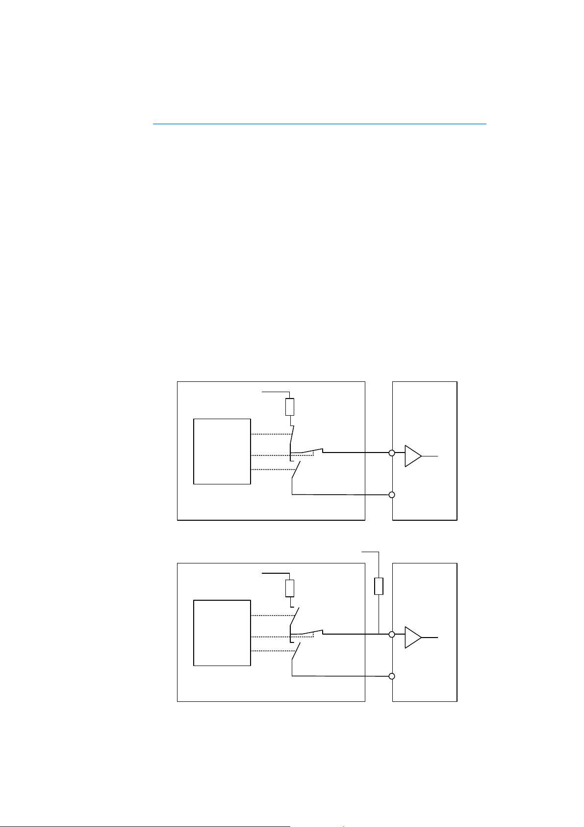
A schematic diagram for a digital output is shown in Fig. 3-6 on page 39.
S1 is a slow switch to select the "Output Mode".
S3 is a slow switch to cut off the signal.
S2 is a fast low-side switch to generate the output signal "Digital Output i" in
real-time. In doing so, S3 is closed.
Generation of a digital output signal "Digital Output i":
• The signal that is set in the "Signals" tab through "Output Select" determines the cycle time for S2.
• The pull-up resistor determines the voltage level of the signal. In the column "Output Mode" in the "Signals" tab, you can choose between an
internal pull-up resistor ("Pull-Up to +5 V") and an external pull-up resistor ("Open Collector"), see Fig. 3-6.
• By closing S2, the low-phase of the signal is generated. By opening S2, the
high-phase is generated.
ES5340.2 Electric Drive Simulation Board -User’s Guide 39
Fig. 3-6 Schematic circuit diagram of a digital output
Page 40
Hardware Description ETAS
phi_el
300°
240°
180°
120°
60°
0°
3.3.2 Configuring the Digital Signals
Which signals are assigned to the eight (ES5340.2-M) or six (ES5340.1-S) outputs
is defined in the output multiplexer (see "Output Multiplexers for the Digital
Signals" on page 41).
You can configure the digital channels themselves as follows.
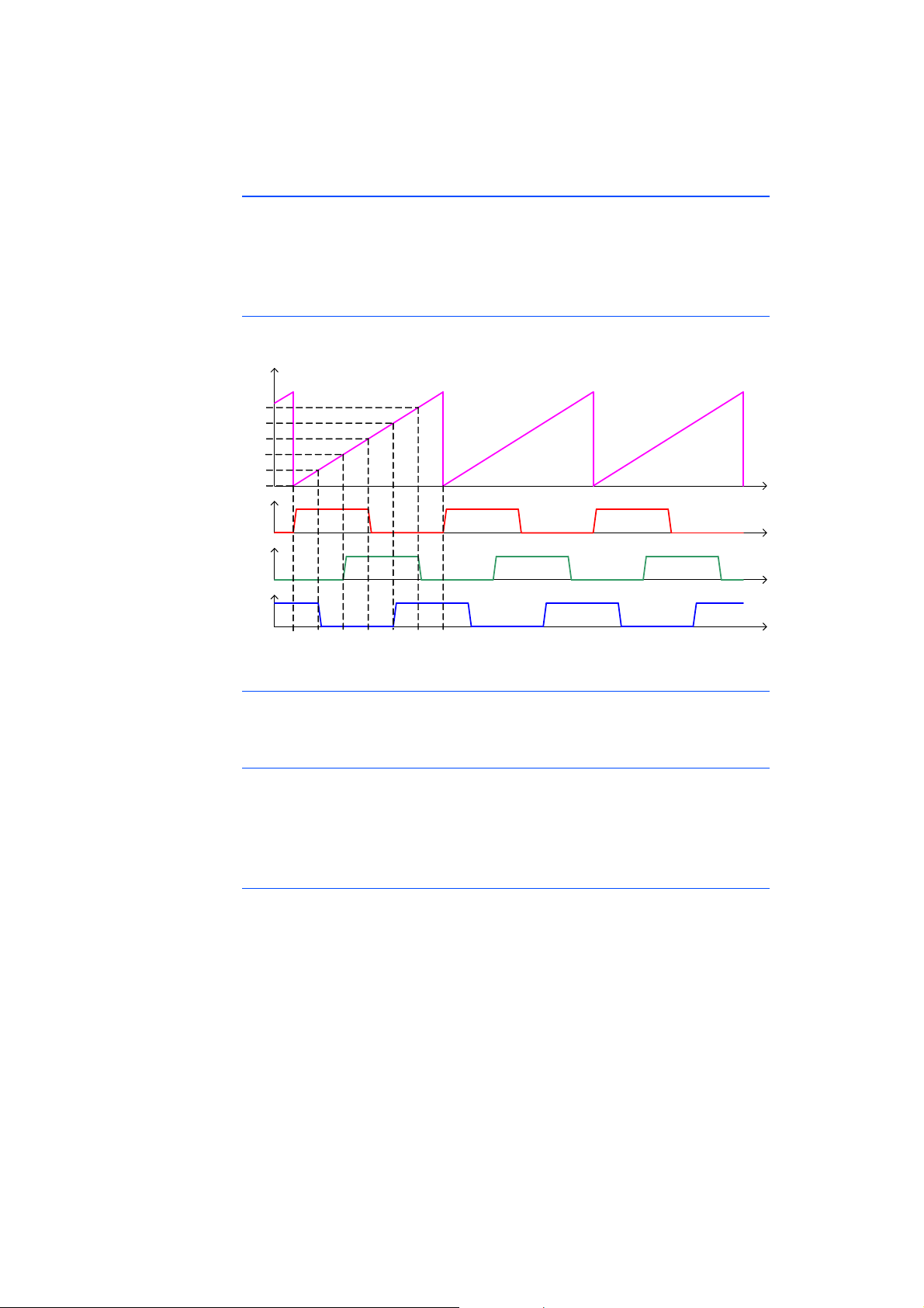
Digital Position Sensor
A digital output configured in this way supplies 3 signals with adjustable rise and
drop-off of the edges (see Fig. 3-7).
Fig. 3-7 Timing for 120° phase-shifted pulses with 180° duration
Digital Direct Out
These outputs enable you to directly stimulate ECU inputs using values from the
model.
Digital Arbitrary
Outputs for arbitrary digital signals can be used to output user-defined signal
patterns (based on the current angle of the simulated electric motor).
This signal pattern can be used, for example, to simulate specific position sensors
and other variables with a direct relationship to the motor angle.
SENT Signals
The generation of signals according to the SENT specification SAE J2716 is possible on four output channels.
ES5340.2 Electric Drive Simulation Board -User’s Guide40
Page 41
ETAS Hardware Description
Note
3.4 Output Multiplexers for the Digital Signals
Each digital output has a multiplexer that can be used to define the signal for this
output.
Sources for the Digital Outputs
The digital output channels can be driven by different sources:
• FPGA model outputs
• Signals of the type "Digital Direct Out" and digital arbitrary signals (incl.
position sensor)
• SENT signals (ES5340-Out-SENT-V3)
• The delayed control signals for the inverter: six inverter control signals
with an adjustable time delay can be output to the ECU for diagnostic
purposes.
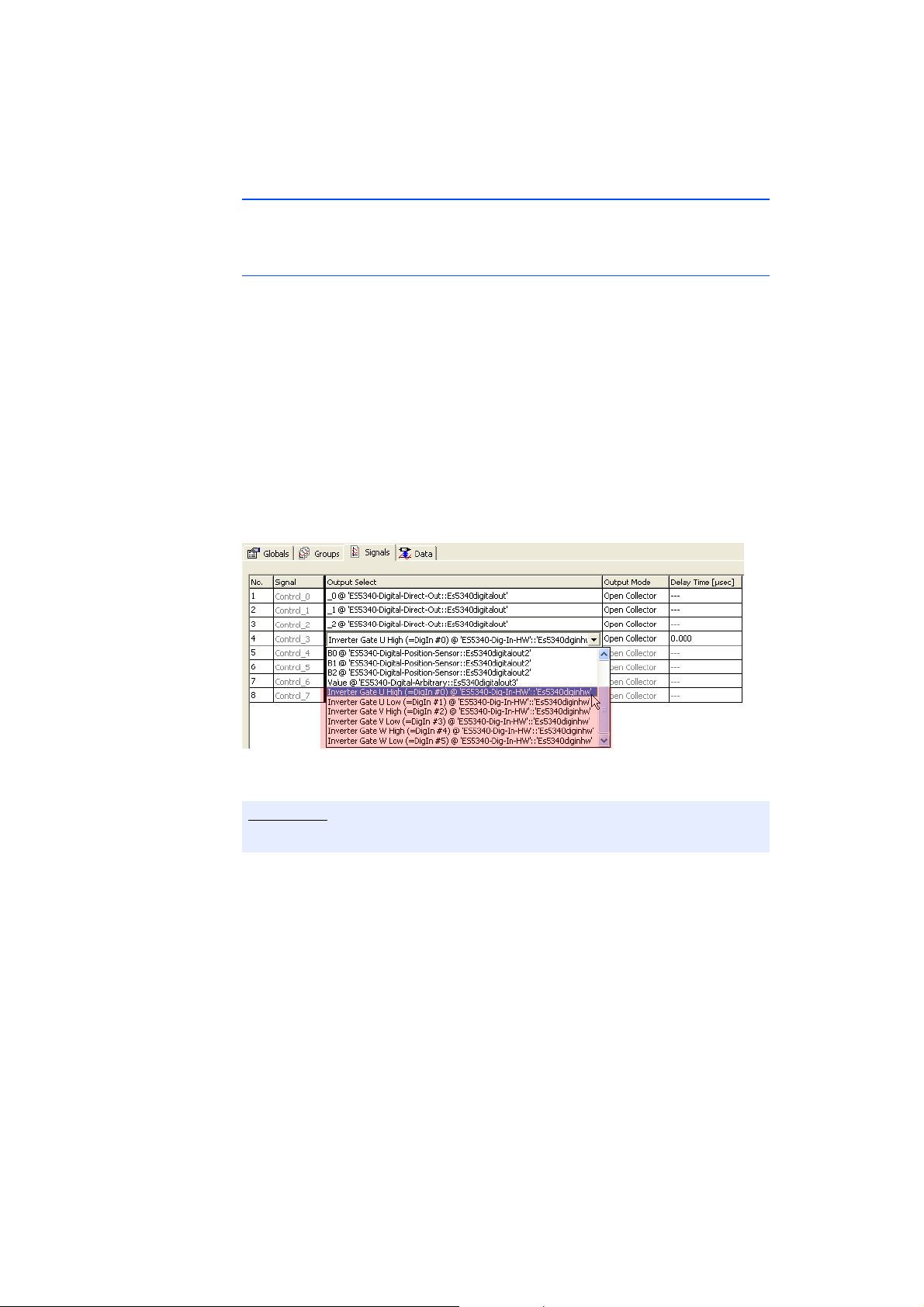
The sources are configured in LABCAR-RTC with the "ES5340-Digital-Out-Mux"
item, "Signals" tab in the "Output Select" column. In addition to the signals
configured by the user, the inverter gate signals are always available here that
can be sent back to the ECU (in some cases, with an adjustable delay).
For a ES5340.2-M, eight signals can be configured for the outputs here; for a
ES5340.1-S, an additional six can be configured.
For slave cards (ES5340.1-S), only "Digital Direct Out" can be selected.
ES5340.2 Electric Drive Simulation Board -User’s Guide 41
Page 42

Hardware Description ETAS
Note
Note
3.5 Analog Inputs
The ES5340.2-M has four inputs for measuring analog signals.
The ES5340.1-S (Slave Board) does not have any analog inputs!
3.5.1 Specification
The operating voltage range for two inputs is 0 to 5 V, with two additional
inputs, it is 0 V to +40 V. All inputs are galvanically isolated and have an elec-
tric strength of ±60 V – the impedance of the inputs is 1 MΩ.
The sampling rate is 500 kSamples/s (software averaging is possible using 2
(n =1 to 8) samples) at a resolution of 12 bits.
3.5.2 Configuring the Analog Inputs
The analog inputs can be used to measure battery voltages and other constant
voltages (control signals).
The type of averaging used for the detected signals can be configured in LABCAR-RTC in the "ES5340-Analog-In" item of the "Globals" tab.
n
3.6 Digital Inputs
The ES5340.2-M has 20 inputs for measuring digital signals.
The ES5340.1-S (Slave Board) does not have any digital inputs!
3.6.1 Specification
The operating voltage range is 0 to +60 V. All inputs are galvanically isolat-
edgalvanically isolated and have an electric strength of ±60 V.
The maximum input frequency is 125 kHz, and the resolution is 8 ns
(125 MHz).
Each input has two independently programmable thresholds for determining
the status of the input ("High" or "Low"). The setting range for these threshold
values is +0 V to +10 V.
ES5340.2 Electric Drive Simulation Board -User’s Guide42
Page 43
ETAS Hardware Description
DAC
Low
ECU
GND
InCh0
Galv. Iso.
DAC
High
Galv. Iso.
High Level
Detection
Low Level
Detection
FPGA
The following illustration shows the schematic circuit diagram of a digital input.
Fig. 3-8 Schematic circuit diagram of a digital input
3.6.2 Configuring the Digital Inputs
Six of the digital inputs are used to measure the gate control of the IGBT of the
inverter; additional inputs can be used to measure DC/DC converter control, for
example.
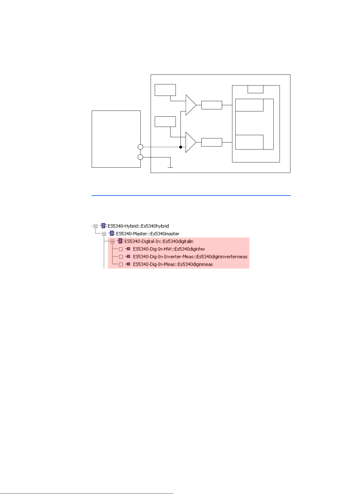
After you add the "ES5340-Digital-In" item to the hardware configuration, the
following items are available:
• ES5340-Dig-In-HW
For configuring the measurement of inverter gate signals
• ES5340-Dig-In-Inverter-Meas
If a model is run on the Real-Time PC, an item must be added for measurement of the inverter gate signals from the ECU; in addition, a mapping of
the current/voltage values to the analog outputs must be created.
The duty cycles and the period of the PWM signals are measured and forwarded to the software model. The measurement itself can be synchronized to an external signal or to the PWM period determined by clock
recovery.
• ES5340-Dig-In-Meas
For general measurement of various properties of digital signals (frequencies, duty cycles etc.).
ES5340.2 Electric Drive Simulation Board -User’s Guide 43
Page 44
Hardware Description ETAS
CAUTION!
Note
Note
Note
3.6.3 Configuration with ES5436.1 to Measure ECU Digital Output Signals
Digital outputs of ECUs are often configured as open emitter or open collector.
In a vehicle, such outputs are connected to small loads.
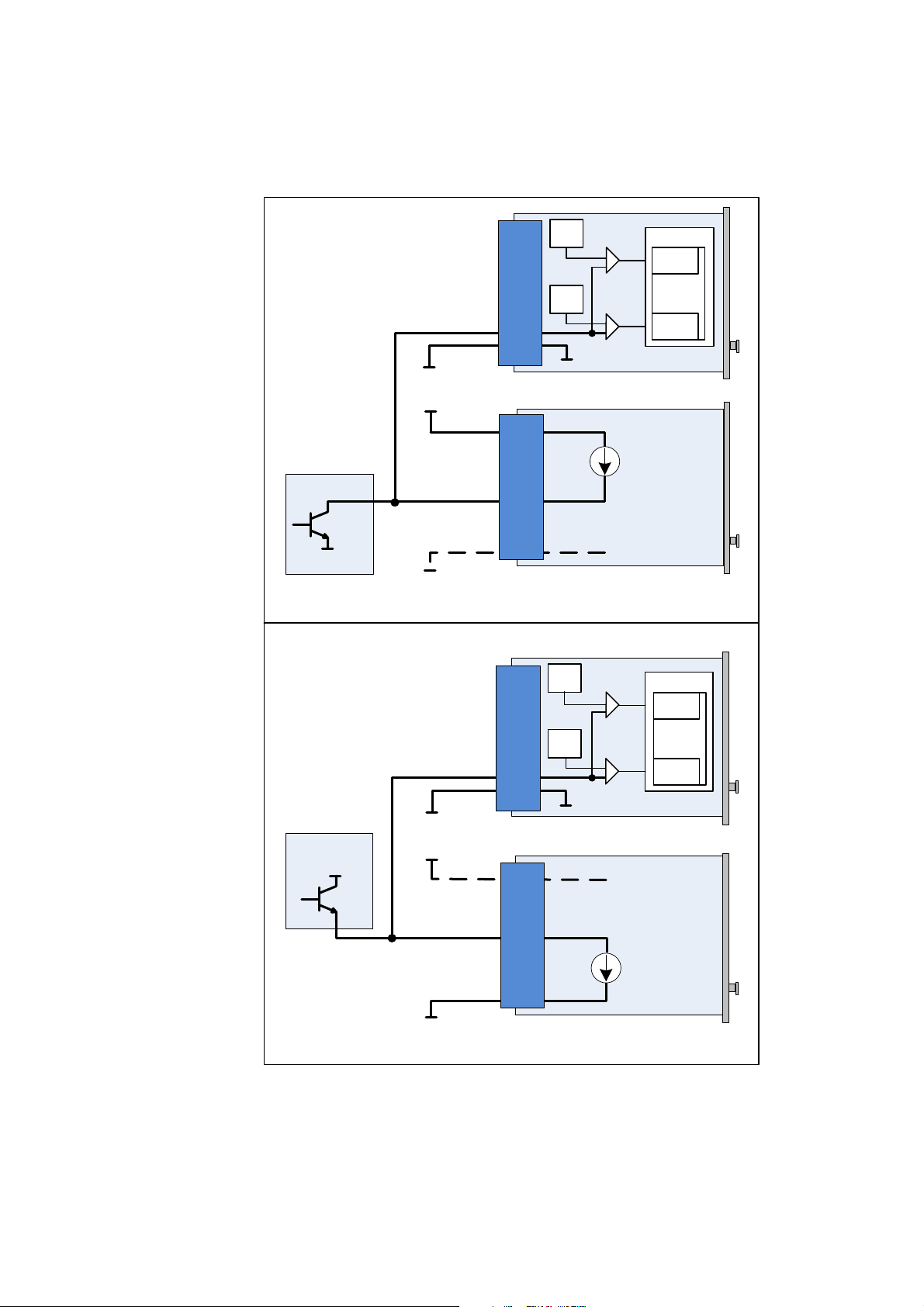
To measure such digital output signals of an ECU in an HiL setup, the ES5436.1
can be used as load simulation and the ES5340 for measurement.
A schematic diagram for the ECU, the ES5340 and the ES5436.1 is shown in
Fig. 3-9 on page 45.
The ES5436.1 has 48 current channels for currents in the range of 5 mA to 150
mA. These current channels can be combined with the 20 digital inputs of the
ES5340.
Before connecting the ES5436.1, read the ES5436.1 User’s Guide.
Technical Data of the ES5436.1 Power Sources
Output Data
Output current 5 mA to 150 mA
Output voltage Passive circuit
Accuracy +/- 3 mA at 150 mA
Galvanic isolation max. 60 V to ground potential (functional separa-
tion)
Overvoltage protection 60 V abs. max.
Tab. 3-1 Technical data of the power sources
In the idle state (non activated load channel, operation mode "disabled") the
power source’s idle state current is ~70
If the external voltage +VBAT < 6 V the power source doesn’t carry any current.
When connecting the ES5436.1, observe the following note:
The ES5436.1 use cases "Pull-Up“, "Pull-Down“ and "Bipolar“ ( "Bipolar" for Hbridge configuration, see "Configuration as H-Bridge" on page 46) can be configured by software.
For this reason, make sure that +VBAT and -VBAT are always connected.
μ
A.
ES5340.2 Electric Drive Simulation Board -User’s Guide44
Page 45
ETAS Hardware Description
ES5340
-VBAT
Input_n
ES5436
+VBAT
Chan_x
+VBAT_x
X1
-VBAT
-VBAT_x
ECU
+VBAT
ECU with
Open Emitter
Pull-Down Configuration
+VBAT
-VBAT
ECU
-VBAT
ECU with
Open Collector
ES5436
Chan_x
+VBAT_x
-VBAT_x
Pull-Up Configuration
ES5340
-VBAT
DAC
Low
FPGA
Low Level
Detection
Input_n
X1
I/O Connector
High Level
Detection
DAC
High
I/O Connector
High Level
Detection
DAC
High
Low Level
Detection
DAC
Low
FPGA
ES5340.2 Electric Drive Simulation Board -User’s Guide 45
Fig. 3-9 Measurement of digital ECU output signals in the configuration
"Pull-Up" or "Pull-Down" using ES5340 for measurement and
ES5436.1 as load simulation
Page 46
Hardware Description ETAS
Note
Note
Note
ES5436
+VBAT
Chan_x
+VBAT_x/y
-VBAT
-VBAT_x/y
Chan_y
X1
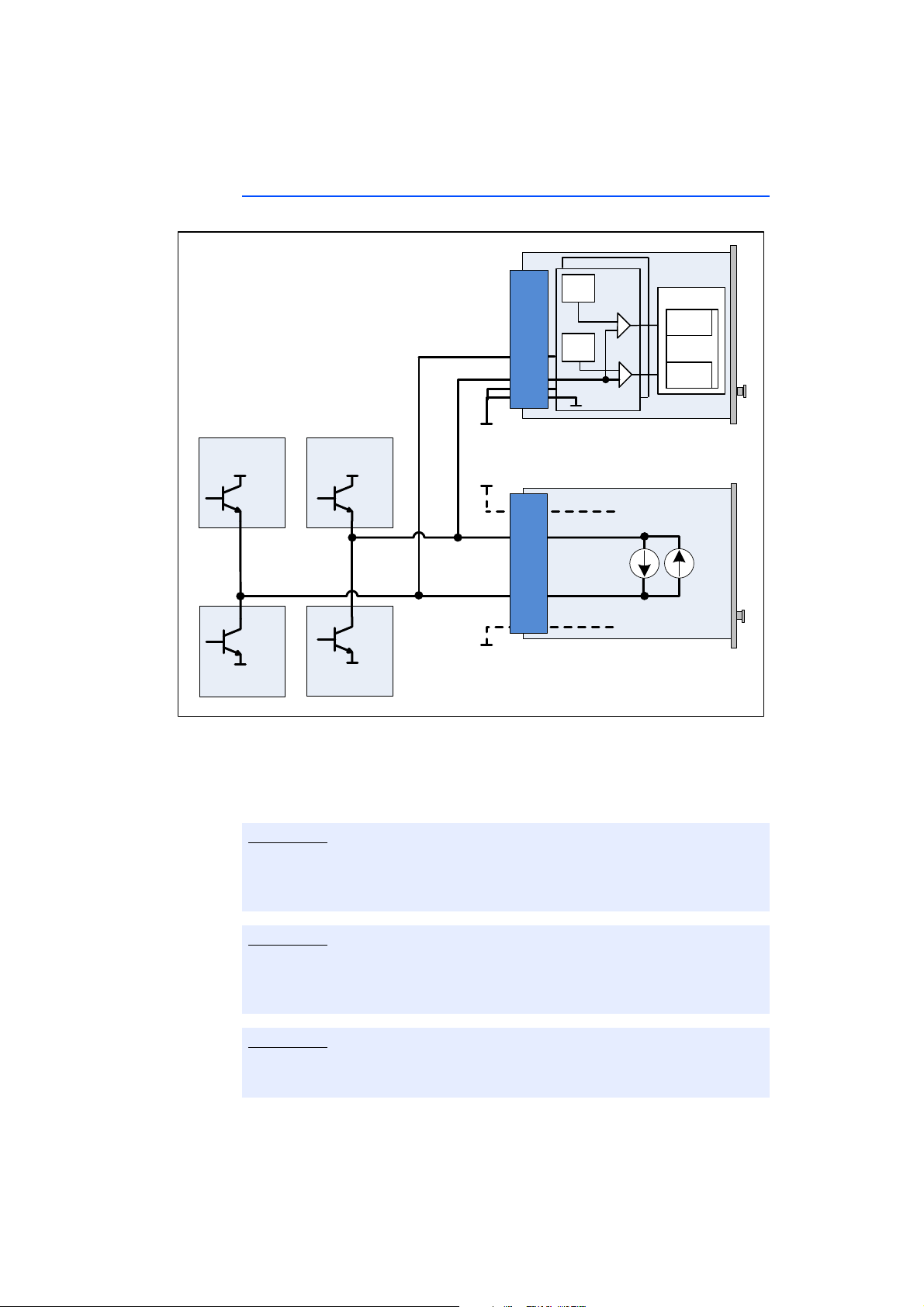
H-Bridge Configuration
ECU
+VBAT
ECU
-VBAT
ECU
+VBAT
ECU
-VBAT
ES5340
-VBAT_n/m
Input_n
Input_m
High Level
Detection
DAC
High
Low Level
Detection
FPGA
DAC
Low
I/O Connector
x20
3.6.4 Configuration as H-Bridge
Fig. 3-10 shows the configuration as H-bridge.
Fig. 3-10 Block diagram for configuration as H-bridge using ES5340 for mea-
suring Chan_x and Chan_y
In case of H-bridge configuration, observe the following notes:
Channel 2i and channel 2i+1 of the ES5436.1 are coupled in each case and can
be used for an H-bridge. Only if channels 2i and 2i+1 are used, there will be a
current flow through the H-bridge.
The ES5436.1 use cases "Pull-Up“, "Pull-Down“ and "Bipolar“ ( for H-bridge)
can be configured by software.
For this reason, make sure that +VBAT and -VBAT are always connected.
For the ES5340, the connections -VBAT_m and -VBAT_n (Fig. 3-10) must be
connected to the same -VBAT potential.
ES5340.2 Electric Drive Simulation Board -User’s Guide46
Page 47
ETAS Hardware Description
V
Low
Hi gh
Sync
V
Low
Hi gh
V
Low
Hi gh
Clock
Direction
V
Low
Hi gh
Engine Speed
α
0 °CA
720 °CA
3.7 RPM Generator
The ES5340.2 Electric Drive Simulation Board has a central RPM Generator that
outputs a speed-specific clock signal.
This RPM unit generates a 16-bit angle value that, in turn, is used for generating
arbitrary signals using analog or digital signal generators.
The maximum speed is:
• 60000 rpm (for 720° crankshaft angle of a combustion engine)
• 30000 rpm (for 360° mechanical angle of an electric motor)
The maximum angle resolution is 0.011 °CA (16 Bit).
3.7.1 Angle Clock Signal
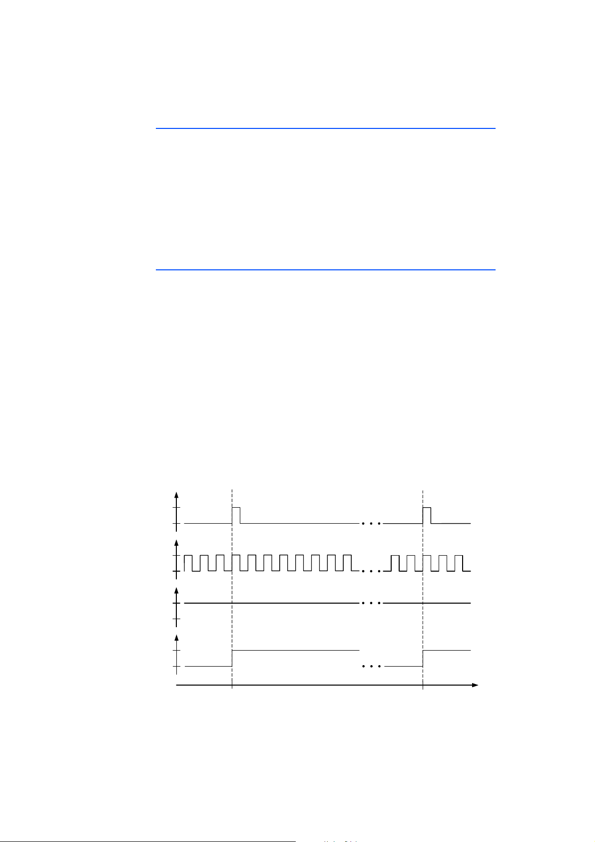
The angle clock signal consists of three signals (see Fig. 3-11):
• The synchronization signal at 0 °CA
• The actual clock signal
• The signal for the direction of rotation (DOR)
A "High" level of the DOR signal means "Rotation with increasing crankshaft angle," while a "Low" level means "Rotation with decreasing crankshaft angle".
One of these three clock signals can be output via a multiplexer to the BNC connection on the front panel (see "Connectors for the Angle Clock Signal
(ES5340.2-M only)" on page 101).
In addition, the engine speed can be output to this connection. This signal is
"High" (= 5 V) if the current crankshaft angle is between 0° and 360° and
"Low" (= 0 V) for crankshaft angles between 360° and 720°.
The following illustration shows the course of the four signals over one camshaft
revolution.
Fig. 3-11 Sync, Clock, Direction and Engine Speed signals
ES5340.2 Electric Drive Simulation Board -User’s Guide 47
Page 48
Hardware Description ETAS
3.7.2 Synchronization
An angle or speed-based synchronization of multiple ES5340.2 Electric Drive
Simulation Boards is possible. For this purpose, any ES5340.2 is configured as the
RPM master, all other ES5340.2 as RPM slaves.
3.7.3 "Master with Angle Adaptation" RPM Mode
To enable synchronization of the RPM unit with a model on the Real-Time PC or
the FPGA model, the RPM unit (as the master) must be adapted to the current
angle of the respective model (angle adaptation).
The speed, angle and the difference between the target angle (model) and current angle are calculated by the model. The RPM unit is then sped up or slowed
down – this ensures that the speed difference is eliminated within the next simulation period (without changing the number of pulses of a "mechanical"
period, 360 °).
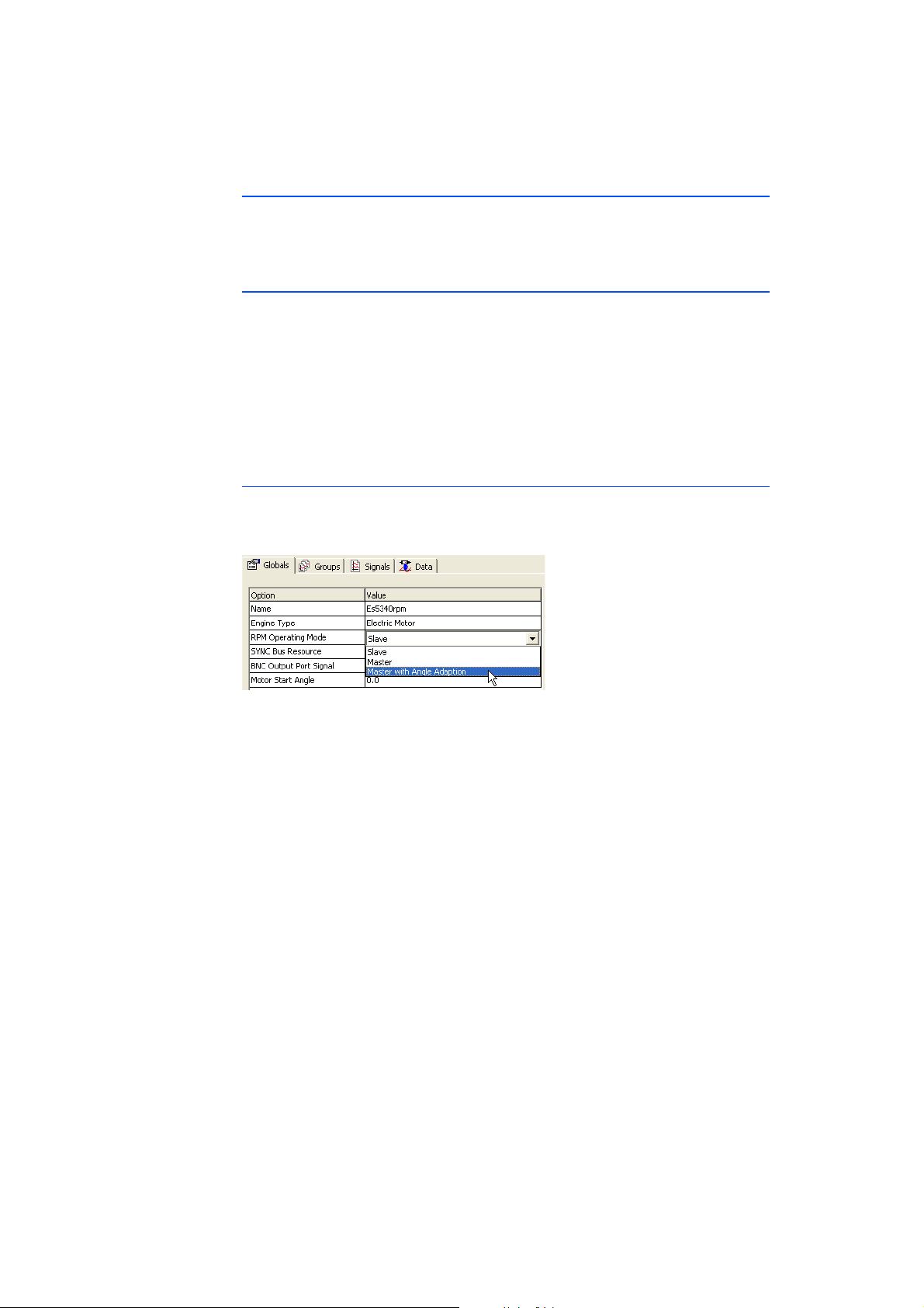
Configuring the RPM unit in LABCAR-RTC
To define the operating mode of the RPM unit, select the item "ES5340-RPM" in
LABCAR-RTC and select the "RPM Operating Mode" option in the "Globals"
tab.
The following settings are possible for the "RPM Operating Mode" option:
• Slave
The ES5340.2 is synchronized to an external angle clock signal.
• Master
The angle clock signal is generated – based on the mechanical angular
velocity – on the ES5340.2 and transmitted to the system hardware on the
SYNC bus.
• Master with Angle Adaptation
The angle clock signal is generated – based on the mechanical angular
velocity and the current angle – on the ES5340.2 and transmitted to the
system hardware on the SYNC bus.
ES5340.2 Electric Drive Simulation Board -User’s Guide48
Page 49
ETAS FPGA Models
Note
6 x
PWM Gate Signal
VehiclePower Stage
phi_mech
omega_mech
load torque
PMSM
phi_elec
3 x
U_back_emf
P_loss
omega_elec
torque_elec
U_DC
3 x
U_phase
3 x
I_phase
6 x
U_switch
6 x
I_element
I_DC
U_Batt0
E-Motor
I_Batt0 I_DC
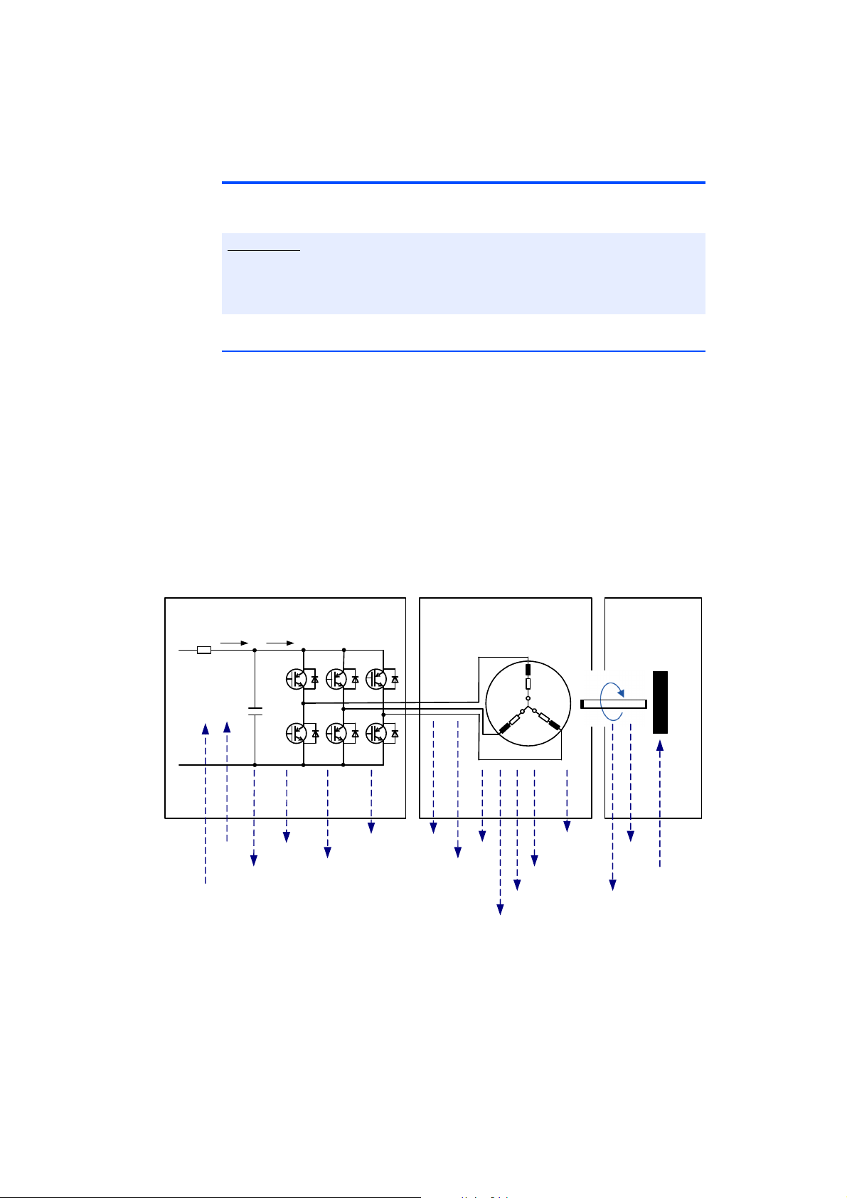
4 FPGA Models
This chapter provides a description of the FPGA models available for purchase for
the ES5340.2 Electric Drive Simulation Board.
If you want to purchase a model separately later, the chapter "Order Information and Scope of Delivery" on page 103 provides additional ordering information.
4.1 Permanent Magnet Synchronous Machine (PMSM) Model
The ES5340.2-M can be expanded by adding a configurable, FPGA-based
inverter/PMSM model. It maps a 3-phase inverter and a permanent magnet synchronous machine (PMSM) with mechanical system.
With great simulation accuracy, the model takes into account all important physical effects required for a reliable test, such as saturation and temperature effects
of engine parameters. In particular, this enables very accurate calculation of the
simulated phase currents.
Within the entire model, calculation takes place using floating-point arithmetic
rather than fixed-point arithmetic. As a result, a very high level of accuracy is
obtained over the entire parameter and simulation range. The FPGA-based
model provides an additional, significant reduction of the cycle times of the
model to 850 ns – compared to approx. 10 μs when running a corresponding
model on a Real-Time PC.
Fig. 4-1 The modeled system
ES5340.2 Electric Drive Simulation Board - User’s Guide 49
Page 50
FPGA Models ETAS
I
UVW
, IDC, U
DC
ϕ, ϕ
T
UH
, TUL , T
VH
T
VL
, TWH , T
WL
Inverter
The inverter has the following tasks:
• Generating AC voltage to operate the 3-phase electric motor from the DC
voltage of the battery (motor operation)
as well as:
• Generating DC voltage to charge the battery from the AC voltage of the
electric motor (generator mode, recuperation)
The inverter is controlled by the hybrid ECU according to the requirement of
torque or speed – depending on the driver command (accelerate, brake) and
battery charge level.
Specifically, this means (see Fig. 4-2):
• Measuring the position (ϕ) and speed (dϕ/dt) of the electric motor
• Measuring the DC-link current (I
phase currents (I
and, as a result,
• Calculating the target voltages at the motor terminals
• and, in turn, calculating the switching phases of the switches in the
inverter branches
, IDC) from/to the electric motor
U,V,W
), the DC-link voltage (UDC) and the
DC
Fig. 4-2 Measurement and control variables of the inverter ECU
Synchronous Motor (PMSM)
The "PMSM" part of the model is used to simulate the phase currents and the
torque of the electric motor.
The PMSM is likewise configured via typical variables, such as the number of pole
pairs and cogging positions. Additional variables such as resistance, inductance,
the magnetic flow and the cogging torque can be changed during run time. For
the PMSM, the power loss of the ohmic components can also be simulated and
their temperature dependence can be calculated.
Mechanical System
For the mechanical connection to the drive train, the FPGA model also includes a
simulation of the spring-mass system. The system is configured with the typical
variables of coefficient of friction, moment of inertia for rotor and load, torsional
rigidity and damping. The load moment of the drive train can be preset and
changed during run-time.
ES5340.2 Electric Drive Simulation Board - User’s Guide50
Page 51

ETAS FPGA Models
4.1.1 Inverter – Parameters, Inputs and Outputs
This section provides the description of all parameters, inputs and outputs of the
"Inverter" part of the model.
Properties of the Inverter Model
The inverter model has the following properties:
• Switches can be high- or low-active
• Simulation of hardware failures (switches always open or closed)
• Simulation of phase voltages U_Phase_X (X = U, V, W) and U_d, U_q
• Simulation of phase voltages on free wheeling (all six inverter switches
open)
• Simulation of DC voltage link
• Simulation of voltages across a switch and of current through the switch
• Simulation of ohmic losses in switches and diodes.
• Information on phase errors (upper and lower switches are open simultaneously)
ES5340.2 Electric Drive Simulation Board - User’s Guide 51
Page 52

FPGA Models ETAS
Note
Parameters
The parameters of the inverter model are configured in LABCAR-RTC in the
"Globals" tab of the item for the FPGA model.
For details about configuring the FPGA model in LABCAR-RTC, refer to the
section "FPGA model" on page 71.
Parameter [unit] Description Default value
Gate Signal Polarity [] "High Active":
switches through when gate is "High"
"Low Active":
switches through when gate is "Low"
R_SW_ON [Ω] Resistance of the switch in conductive
state (20 °C, 68 °F)
U_SW_Fwd [V] Forward voltage across switch in
conductive state (20 °C, 68 °F)
R_D_Fwd [Ω] Resistance of the diode in conductive
state (20 °C, 68 °F)
U_D_Fwd [V] Forward voltage across diode in con-
ductive state (20 °C, 68 °F)
T_Switch [s] Switching time (for calculating the
ohmic losses)
a_Inv [1/K] Temperature coefficient of the ohmic
resistance of switch and diode
R_Batt [Ω] Internal resistance of the battery for the
inverter voltage
C_DC [mF] Capacitance of DC voltage link 0.5
"High Active"
0.001
0.7
0.001
0.7
0.000005
0.00393
0.5
Tab. 4-1 Parameters of the inverter model
ES5340.2 Electric Drive Simulation Board - User’s Guide52
Page 53

ETAS FPGA Models
Inputs
In addition to the voltage and temperature of the inverter, you can configure
signals here that you can use simulate failures of the inverter during runtime
(switch getting stuck on "High" or "Low").
You can connect the inputs of the inverter model to other models (in the Connection Manager of LABCAR-IP) or stimulate them in the Signal Center in
LABCAR-EE.
Input [unit] Description Default value
Fail_HS_X (X=U,V,W) []Gate failure highside switch phase X:
0 = no failure
1 = stuck on "Low"
2 = stuck on "High"
Fail_LS_X (X=U,V,W) [] Gate failure lowside switch phase X:
0 = no failure
1 = stuck on "Low"
2 = stuck on "High"
U_Batt0 [V] Input voltage of the inverter 0.0
Theta_Inv [°C] Temperature of the inverter 20.0
0
0
Tab. 4-2 Inputs of the inverter model
ES5340.2 Electric Drive Simulation Board - User’s Guide 53
Page 54

FPGA Models ETAS
Outputs
You can connect the outputs of the inverter model with analog or digital outputs
(in LABCAR-RTC) and to other models (in the Connection Manager of
LABCAR-IP).
Output [unit] Description Signal available as
multiplexer input
U_Phase_X (X=U,V,W)
[V]
U_d [V] Voltage in d direction Analog MUX
U_q [V] Voltage in q direction Analog MUX
I_DC [A] Total inverter current Analog MUX
U_DC [V] Inverter voltage Analog MUX
I_element_XH (X=U,V,W)
[A]
I_element_XL (X=U,V,W)
[A]
U_switch_XH (X=U,V,W)
[V]
U_switch_XL (X=U,V,W)
[V]
P_Loss_Inv [W] Ohmic losses in inverter - *
Error [] Error register
* Model output (can be used by another model or managed in the Connection
Manager (LABCAR-IP) and the Signal Center (LABCAR-EE))
Voltage Phase X Analog MUX
Current through upper
switch phase X
Current through lower
switch phase X
Voltage through upper
switch phase X
Voltage through lower
switch phase X
If upper and lower switches
are at "High" simultaneously, a phase error occurs
Bit 0: Phase U
Bit 1: Phase V
Bit 2: Phase W
Analog MUX
Analog MUX
Analog MUX
Analog MUX
- *
Tab. 4-3 Outputs of the inverter model
ES5340.2 Electric Drive Simulation Board - User’s Guide54
Page 55

ETAS FPGA Models
4.1.2 PMSM – Parameters, Inputs and Outputs
This section provides the description of all parameters, inputs and outputs of the
"PMSM" part of the model.
Properties of the PMSM Model
The PMSM model has the following properties:
• Simulation of phase currents I_Phase_X (X = U, V, W) and I_d, I_q
• Simulation of counter emf
• Consideration of cogging torque when simulating the torque of the electrical motor
• Output of status signal (U_phase_U > U_phase_V) for the matching of
position sensors
• Simulation of ohmic losses
• Setting of simulation start values for I_d and I_q
• R_d, R_q, L_d, L_q and magnetic flux can be changed in real-time
Parameters
The parameters of the electric motor model are configured in LABCAR-RTC in
the "Globals" tab of the item for the FPGA model.
Parameter [unit] Description Default value
Pole Pairs [] Number of pole pairs of the electric
motor
Ncog [] Number of cogging positions 18
T_cm [Nm] Maximum amount of cogging torque 0.0
Id Init [A] Initial value of I_d
(see Tab. 4-6 on page 56)
Iq Init [A] Initial value of I_q
(see Tab. 4-6 on page 56)
a_M [1/K] Temperature coefficient of R_d and
R_q
Tab. 4-4 Parameters of the PMSM model
12
0.0
0.0
0.00430
ES5340.2 Electric Drive Simulation Board - User’s Guide 55
Page 56

FPGA Models ETAS
Inputs
You can connect the inputs of the PMSM model to other models (in the Connection Manager of LABCAR-IP) or stimulate them in the Signal Center in
LABCAR-EE.
Input [unit] Description Default value
Rd [Ω] Coil resistance in d direction 0.0125
Rq [Ω] Coil resistance in q direction 0.0125
Ld [H] Coil inductance in d direction 0.000211
Lq [H] Coil inductance in q direction 0.000211
Psi [Vs] Magnetic flux 0.0382
Theta_M [°C] Engine temperature 20.0
Tab. 4-5 Inputs of the PMSM model
Outputs
You can connect the outputs of the PMSM model with analog or digital outputs
(in LABCAR-RTC) and to other models (in the Connection Manager of
LABCAR-IP).
Output
[unit]
I_d [A] Current in d direction Analog MUX
I_q [A] Current in q direction Analog MUX
I_phase_X
(X=U,V,W) [A]
U_back_EMF_X
(X=U,V,W) [V]
ZeroPos [] Signal is active if phase voltage
T_el [Nm] Torque of electric motor -
P_Loss_M [W] Ohmic losses of the motor -
Tab. 4-6 Outputs of the PMSM Model
Description Signal available as
multiplexer input
Current Phase X Analog MUX
Voltage X back EMF Analog MUX
Digital_MUX
U_Phase_U > U_Phase_V
ES5340.2 Electric Drive Simulation Board - User’s Guide56
Page 57

ETAS FPGA Models
4.1.3 Mechanical System – Parameters, Inputs and Outputs
This section provides the description of all parameters, inputs and outputs of the
"Mechanical system" part of the model.
Properties of the Mechanical Model
The mechanical model has the following properties:
• Simulation of angle and angular velocity of the rotor and the electrical
field
• Resulting mechanical torque
Parameters
The parameters of the mechanical system model are configured in LABCAR-RTC
in the "Globals" tab of the item for the FPGA model.
Parameter [unit] Description Default
value
f [Nms] Coefficient of friction of the electric
1.7
motor
J_E [kgm
J_L [kgm
2
] Moment of inertia of the rotor 0.12
2
] Moment of inertia of the load
0.10
(powertrain etc.)
C [Nm/rad] Torsional stiffness ("spring constant")
1500000
of the "spring" between rotor and
load.
D [Nms/rad] Damping of the "spring" between
100
rotor and load.
Phi_mech_init [°] Initial mechanical angle 0.0
Omega_mech_init [1/s] Initial mechanical speed 0.0
Tab. 4-7 Parameters of the mechanical model
Inputs
You can connect the inputs of the mechanical model to other models (in the
Connection Manager of LABCAR-IP) or stimulate them in the Signal Center in
LABCAR-EE.
Input [unit] Description Default
value
T_L [Nm] Load moment
Tab. 4-8 Inputs of the mechanical model
ES5340.2 Electric Drive Simulation Board - User’s Guide 57
Page 58

FPGA Models ETAS
Outputs
You can connect the outputs of the mechanical model with analog or digital
outputs (in LABCAR-RTC) and to other models (in the Connection Manager of
LABCAR-IP).
Output
[unit]
Omega_mech [1/s] Angular velocity: rotor Analog MUX
Phi_mech [°] Angle: rotor Analog MUX
Omega_el [1/s] Angular velocity: electrical field Analog MUX
Phi_el [°] Angle: electrical field Analog MUX
T_mech [Nm] Resulting mechanical torque Analog MUX
Tab. 4-9 Outputs of the mechanical model
Description Signal available as
multiplexer input
ES5340.2 Electric Drive Simulation Board - User’s Guide58
Page 59
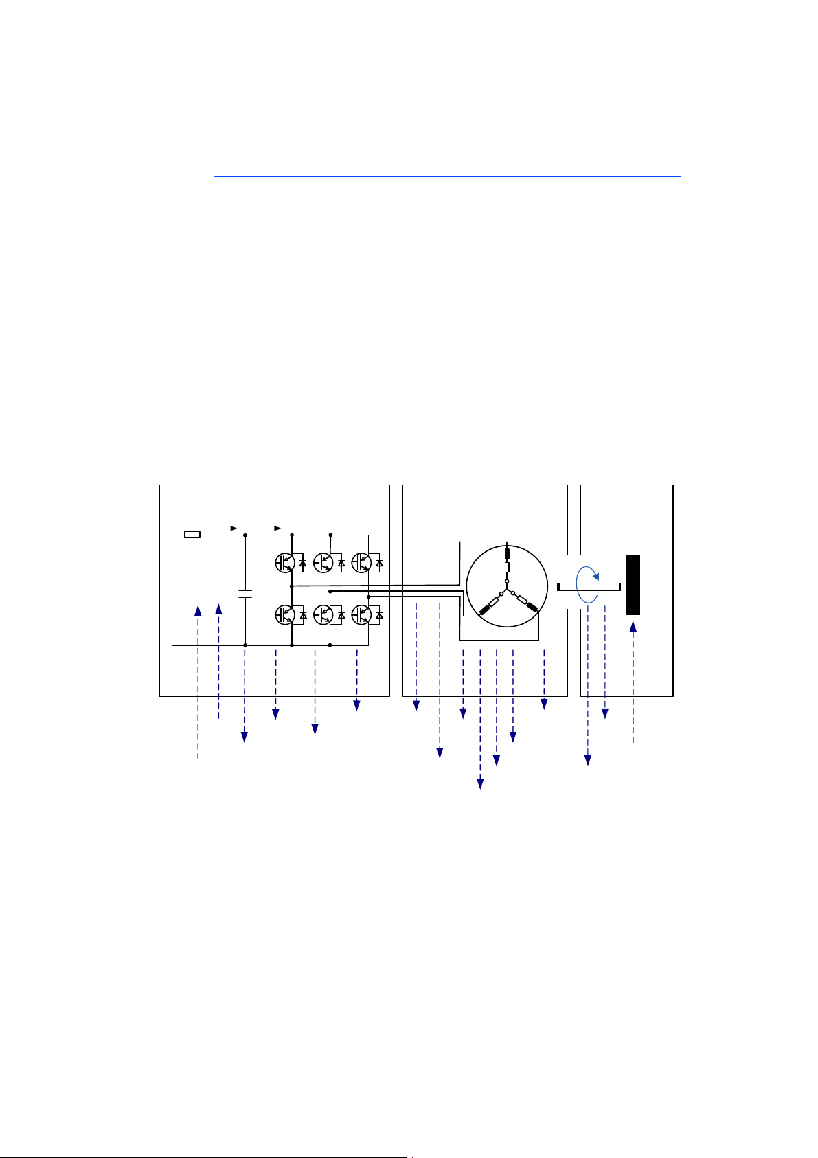
ETAS FPGA Models
6 x
PWM Gate Signal
VehiclePower Stage
phi_mech
omega_mech
load torque
Induction Machine
phi_elec
3 x
U_ind
P_loss
omega_elec
torque_elec
U_DC
3 x
U_phase
6 x
U_switch
6 x
I_element
I_DC
U_Batt0
E-Motor
3 x
I_stator
3 x
I_rotor
I_Batt0 I_DC
4.2 Induction Machine (IM) Model
The FPGA model of an induction machine (IM) is build up out of a three-phase
inverter and an induction machine including mechanics. Many experiences out of
the development of electrical drives took influence on this model. So it is able to
simulate the essential physical effects needed for reliable tests, like temperature
effects or saturations of motor parameters. It is build up according to a balanced
behavior between runtime and accuracy.
Within the whole model calculations are made with floating-point arithmetic
which results in a very high accuracy over the whole parameter- and simulation-area. With the FPGA based model the model step sizes are once more
reduced drastically to 850 ns – according to about 10 μs of a related model executed on a real-time PC. This makes it possible to detect a PWM signal via Hardware with a high accuracy and directly use this signal in the inverter model.
The model consists of three parts:
•Inverter
• Induction machine (IM)
• Mechanical load.
Fig. 4-3 The modeled system
Inverter Model
The parameterization of the inverter is done by using typical values like switching
times, polarity or resistances of switches and diodes. For every switch it is possible to parameterize the failure states “Open” and “Closed”. Also the “freewheeling” can be simulated, when all six switches are opened.
For the whole inverter also the temperature dependent power loss of ohmic
components is considered. The inputs of the inverter include the inner resistance
of the battery as well as the intermediate circuit capacitance, which makes it
possible to simulate the intermediate circuit voltage.
ES5340.2 Electric Drive Simulation Board - User’s Guide 59
Page 60

FPGA Models ETAS
IM Model
The parameterization of the induction machine is done by using typical values
like pole pair number or temperature coefficient. Other values like resistances,
inductivities and temperature are changeable during runtime. This allows for a
very accurate simulation of phase currents and electrical torque.
Mechanical Model
For the mechanical connection to the drive train, the spring-damper system is
also simulated inside the model. The parameterization of the mechanical model
is done by using typical values like friction coefficient, inertias for rotor and load,
torsional stiffness and damping. The load torque of the drive train can be
changed by the user during runtime.
4.2.1 Inverter – Parameters, Inputs and Outputs
Parameters
Parameter [unit] Description Value range Default
value
Gate Signal
Polarity
U_SW_Fwd [V] Forward voltage across
U_D_Fwd [V] Forward voltage across free-
T_Switch [s] Switching time 0.0000002 -
a_Inv [1/K] Temperature coefficient of
R_Batt [Ω] Internal resistance of battery 0.01 - 10.0 0.5
C_DC [mF] Capacitance of intermediate
Tab. 4-10 Parameters of the inverter model
"High Active": Conducting
when gate is "High"
"Low Active": Conducting
when gate is "Low"
switch in conductive state
(20 °C, 68 °F)
wheeling diode in conductive
state (20 °C, 68 °F)
the ohmic resistance of the
inverter
circuit
Low Active,
High Active
0.0 - 3.0 0.7
0.0 - 3.0 0.7
0.000001
0.0 - 0.01 0.00393
0.01 - 10.0 0.5
High Active
0.0000005
ES5340.2 Electric Drive Simulation Board - User’s Guide60
Page 61

ETAS FPGA Models
Inputs
Input [unit] Description Value range Default
value
Fail_HS_X
(X=U,V,W) []
Gate failure highside switch
phase X:
0, 1, 2 0
0 = no failure
1 = stuck on "Low"
2 = stuck on "High"
Fail_LS_X
(X=U,V,W) []
Gate failure lowside switch
phase X:
0, 1, 2 0
0 = no failure
1 = stuck on "Low"
2 = stuck on "High"
U_Batt0 [V] Input voltage of the inverter 0.0..1500.0 0.0
Theta_Inv [°C] Temperature of the inverter -50.0..200.0 20.0
R_SW_ON [Ω] Resistance of the switch in
0.0..0.05 0.001
conductive state (20 °C, 68 °F)
R_D_Fwd [Ω] Resistance of the diode in
0.0..0.05 0.001
conductive state (20 °C, 68 °F)
Tab. 4-11 Inputs of the inverter model
Outputs
Output
[unit]
I_Batt -1500 /
U_DC [V] 0 / 0..1500 1500 / 0..1500 0 / 0 10.0 / 10.0
I_DC [A] -1500 /
I_element_XH
(X=U,V,W) [A]
I_element_XL
(X=U,V,W) [A]
U_switch_XH
(X=U,V,W) [V]
U_switch_XL
(X=U,V,W) [V]
U_phase
(X=U,V,W) [V]
P_loss_Inv [W] 4000 /
Model Value
(min)
default / range
-1500..1500
-1500..1500
-1500 /
-1500..1500
-1500 /
-1500..1500
-150 /
-150..1500
-150 /
-150..1500
-150 /
-150..1500
0.0..20000
Model Value
(max)
default / range
1500 /
-1500..1500
1500 /
-1500..1500
1500 /
-1500..1500
1500 /
-1500..1500
1500 /
-1500..1500
1500 /
-1500..1500
1500 /
-1500..1500
4000 /
0.0..20000
DAC Voltage
(min)
default / min
-10.0 / -10.0 10.0 / 10.0
-10.0 / -10.0 10.0 / 10.0
-10.0 / -10.0 10.0 / 10.0
-10.0 / -10.0 10.0 / 10.0
-1.0 /-1.0 10.0 / 10.0
-1.0 /-1.0 10.0 / 10.0
-1.0 /-1.0 10.0 / 10.0
- -
DAC Voltage
(max)
default / max
Tab. 4-12 Outputs of the inverter model
ES5340.2 Electric Drive Simulation Board - User’s Guide 61
Page 62

FPGA Models ETAS
4.2.2 Induction Machine – Parameters, Inputs and Outputs
Parameters
Parameter
[unit]
Description Value range Default
value
Pole Pairs [] Number of pole pairs 1 - 16 12
I_stator_X_Init
Initial current in stator phases -1500.. +1500 0
(X=U,V,W) [A]
I_rotor_X_Init
Initial current in rotor phases -1500.. +1500 0
(X=U,V,W) [A]
a_M [1/K] Temperature coefficient of
0.0..0.01 0.00430
ohmic resistance of the stator
coils
Tab. 4-13 Parameters of the IM model
Inputs
Input [unit] Description Value range Default
value
Rs1 [Ω] Stator coil resistance at 20 °C 0.0..1.0 0.1
Rs2 [Ω] Rotor coil resistance at 20 °C 0.0..1.0 0.1
Lm [H]
Effective inductance 0.0..1.0 0.025
Ls1 [H] Stator coil inductance 0.0..0.1 0.001
Ls2 [H] Rotor coil inductance 0.0..0.1 0.001
Theta_M [°C] Engine temperature -50.0..200.0 20.0
Tab. 4-14 Inputs of the IM model
ES5340.2 Electric Drive Simulation Board - User’s Guide62
Page 63

ETAS FPGA Models
Outputs
Output
[unit]
I_stator_X
Model value
(min)
default / range
Model value
(max)
default / range
DAC voltage
(min)
default / min
-1500 +1500 -10.0 / -10.0 10.0 / 10.0
(X=U,V,W) [A]
I_rotor_X
-1500 +1500 -10.0 / -10.0 10.0 / 10.0
(X=U,V,W) [A]
U_ind_X
-1500 +1500 -10.0 / -10.0 10.0 / 10.0
(X=U,V,W) [V]
T_el [Nm] -1000 /
-1000..1000
P_loss_M [W] 4000 / 0.0 -
20000
1000 /
-1000..1000
4000 / 0.0 20000
-10.0 / -10.0 10.0 / 10.0
- -
Tab. 4-15 Outputs of the IM model
4.2.3 Mechanical System – Parameters, Inputs and Outputs
Parameters
Parameter [unit] Descriptions Value range Default
f [Nms] Friction coefficient of
0.0 - 10.0 1.7
E-machine
2
J_E [kgm
J_L [kgm
] Inertia of rotor 0.0 - 1.0 0.12
2
] Inertia of load 0.0 - 10.0 0.10
C [Nm/rad] Torsional stiffness 0.0 -
10000000.0
D [Nms/rad] Damping between rotor and
0.0..1000.0 100.0
load
Phi_mech_Init [°] Inital mechanical angle 0.0..360.0 0.0
Omega_mech_Init
[rad/s]
Initial mechanical velocity -833.333..
+833.333
DAC voltage
(max)
default / max
value
1500000.0
0.0
Tab. 4-16 Parameters of the mechanical model
Inputs
Input [unit] Description Value Range Default
value
T_L [Nm] Torque of electric motor -1000.0..1000.0 0.0
Tab. 4-17 Inputs of the mechanical model
ES5340.2 Electric Drive Simulation Board - User’s Guide 63
Page 64

FPGA Models ETAS
Outputs
Output
[unit]
Omega_mech
[rad/s]
Phi_mech
[°]
Omega_el
[rad/s]
Phi_el
[°]
T_mech
[Nm]
Model value
(min)
default / range
-50000 /
-50000..50000
0 / 0..360 360 / 0..360 0 / -10.0 10.0 / 10.0
-10000 /
-50000..50000
0 / 0..360 360 / 0..360 0 / -10.0 10.0 / 10.0
-2000 /
-2000..2000
Model value
(max)
default / range
50000 /
-50000..50000
10000 /
-50000..50000
2000 /
-2000..2000
Tab. 4-18 Outputs of the mechanical model
DAC voltage
(min)
default / min
-10.0 / -10.0 10.0 / 10.0
-10.0 / -10.0 10.0 / 10.0
-10.0 / -10.0 10.0 / 10.0
DAC voltage
(max)
default / max
ES5340.2 Electric Drive Simulation Board - User’s Guide64
Page 65

ETAS Configuring the Hardware in LABCAR-RTC
5 Configuring the Hardware in LABCAR-RTC
This chapter provides a description of the procedure for configuring the hardware in LABCAR-RTC.
• "General Settings" on page 66
This section provides a description of a few basic settings of the hardware
configuration.
– ""ES5340-Master" item" on page 66
– "Measuring the Gate Trigger Signals" on page 67
– "RPM Unit" on page 69
• "Integration of the Model" on page 71
The next step consists of configuring the connections to a model.
– "FPGA model" on page 71
– "Software Model" on page 75
• "I/O Configuration" on page 81
This chapter provides a description of the configuration of the input and
output channels of the ES5340.2.
– "Position sensors" on page 81
– "Analog Outputs" on page 84
– "Digital Outputs" on page 86
– "Analog Inputs" on page 89
– "Digital Inputs" on page 90
– "Signal Output via the Analog Multiplexer" on page 92
– "Signal Output via the Digital Multiplexer" on page 94
ES5340.2 Electric Drive Simulation Board - User’s Guide 65
Page 66
Configuring the Hardware in LABCAR-RTC ETAS
5.1 General Settings
This section provides a description of a few basic settings of the hardware configuration.
In particular, they include:
• "Creating an "ES5340-Master" Item" on page 66
• "Adding an "ES5340-Digital-In" Item" on page 67
• "Adding an "ES5340-Dig-In-HW" Item" on page 67
• "Assigning Inverter Gates to Measurement Channels" on page 68
• "Creating an "ES5340-RPM" Item" on page 69
5.1.1 "ES5340-Master" item
Creating an "ES5340-Master" Item
1. In LABCAR-IP, select Project → RTIO Editor.
The editor of LABCAR-RTC is opened.
2. Select the "RTPC" system.
3. Right-click and select Add Item.
4. In the selection dialog, select the item "ES5340Hybrid".
5. Click OK.
The item is added.
ES5340.2 Electric Drive Simulation Board - User’s Guide66
Page 67
ETAS Configuring the Hardware in LABCAR-RTC
Note
6. In the same way, add an "ES5340-Master" item to
the "ES5340-Hybrid" item.
7. Select File → Save.
Error messages in the monitor window indicate that
the configuration of the hardware is not yet complete.
5.1.2 Measuring the Gate Trigger Signals
To measure the PWM control signals for the inverter, you have to add an item for
measuring digital signals.
Adding an "ES5340-Digital-In" Item
1. Right-click the "ES5340-Master" item and select
Add Item.
2. In the list, select the "ES5340-Digital-In" item and
click OK.
The item is added.
Adding an "ES5340-Dig-In-HW" Item
1. Right-click the "ES5340-Digital-In" item and select
Add Item.
ES5340.2 Electric Drive Simulation Board - User’s Guide 67
Page 68
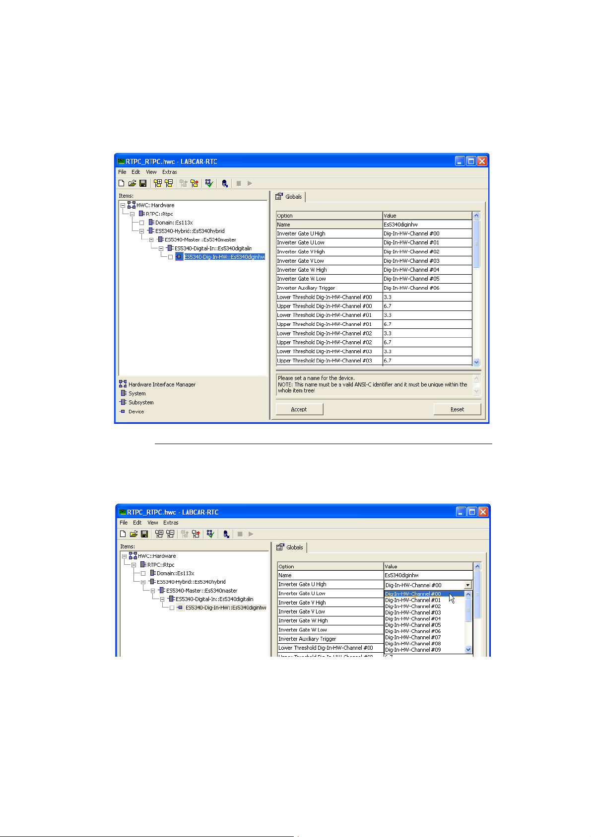
Configuring the Hardware in LABCAR-RTC ETAS
2. In the list, select the "ES5340-Dig-In-HW" item and
click OK.
The item is added.
Assigning Inverter Gates to Measurement Channels
For the ES5340.2-M, we assume that six gate signals are present (two for each
phase).
1. Assign the gate signals to the desired measurement
channels.
When measuring the gate control, for each measurement channel, one upper and one lower voltage level can be specified, below (above) which the
signal is identified as "low" ("high").
ES5340.2 Electric Drive Simulation Board - User’s Guide68
Page 69
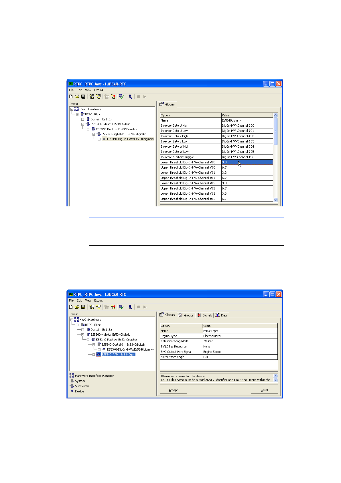
ETAS Configuring the Hardware in LABCAR-RTC
2. Edit the option for the corresponding threshold values accordingly.
5.1.3 RPM Unit
The RPM unit is used to generate speed and angle information that is required
by position sensors and other angle-synchronous signals.
Creating an "ES5340-RPM" Item
1. Right-click the "ES5340-Master" item and select
Add Item.
2. In the list, select the "ES5340-RPM" item and click
OK.
The item is added.
ES5340.2 Electric Drive Simulation Board - User’s Guide 69
Page 70
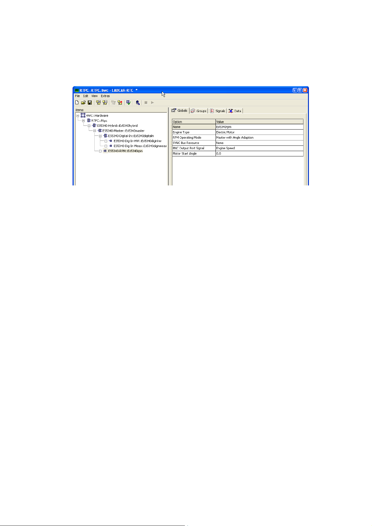
Configuring the Hardware in LABCAR-RTC ETAS
3. For the specific application "Electric Motor", configure the settings in the "Globals" tab as shown:
The ES5340.2 can thus be configured as the RPM
master for other hardware.
ES5340.2 Electric Drive Simulation Board - User’s Guide70
Page 71
ETAS Configuring the Hardware in LABCAR-RTC
Note
5.2 Integration of the Model
The next step consists of configuring the connections to a model.
This requires different measures depending on the type of the model:
• FPGA model
This model is run autonomously on the ES5340.2 Electric Drive Simulation
Board and is configured in LABCAR-OPERATOR.
The FPGA model is an optional component of the ES5340.2 Electric Drive
Simulation Board and must be ordered separately (see "Order Information
and Scope of Delivery" on page 103).
• Software model
A software model (ASCET, Simulink or C code) is run on the Real-Time PC,
synchronized with the PWM signals from the ECU.
Specifically, the following measures are described:
• "FPGA model" on page 71
– "Adding the FPGA Model in LABCAR-RTC" on page 71
– "Configuring the Model Parameters" on page 73
– "Configuring the Value Ranges" on page 74
– "Determining Default Values" on page 75
– "Configuring Outputs for Current/Voltage Sensors" on page 77
• "Software Model" on page 75
– "Configuring the Inverter Gate Measurement" on page 75
– "Adding Analog Outputs ("Direct out")" on page 77
– "Adding Analog Outputs (for Predicted Values)" on page 78
5.2.1 FPGA model
For configuring the FPGA model, you first have to add the corresponding item.
Adding the FPGA Model in LABCAR-RTC
1. Select the "ES5340-Master" item and click Add
Item.
ES5340.2 Electric Drive Simulation Board - User’s Guide 71
Page 72
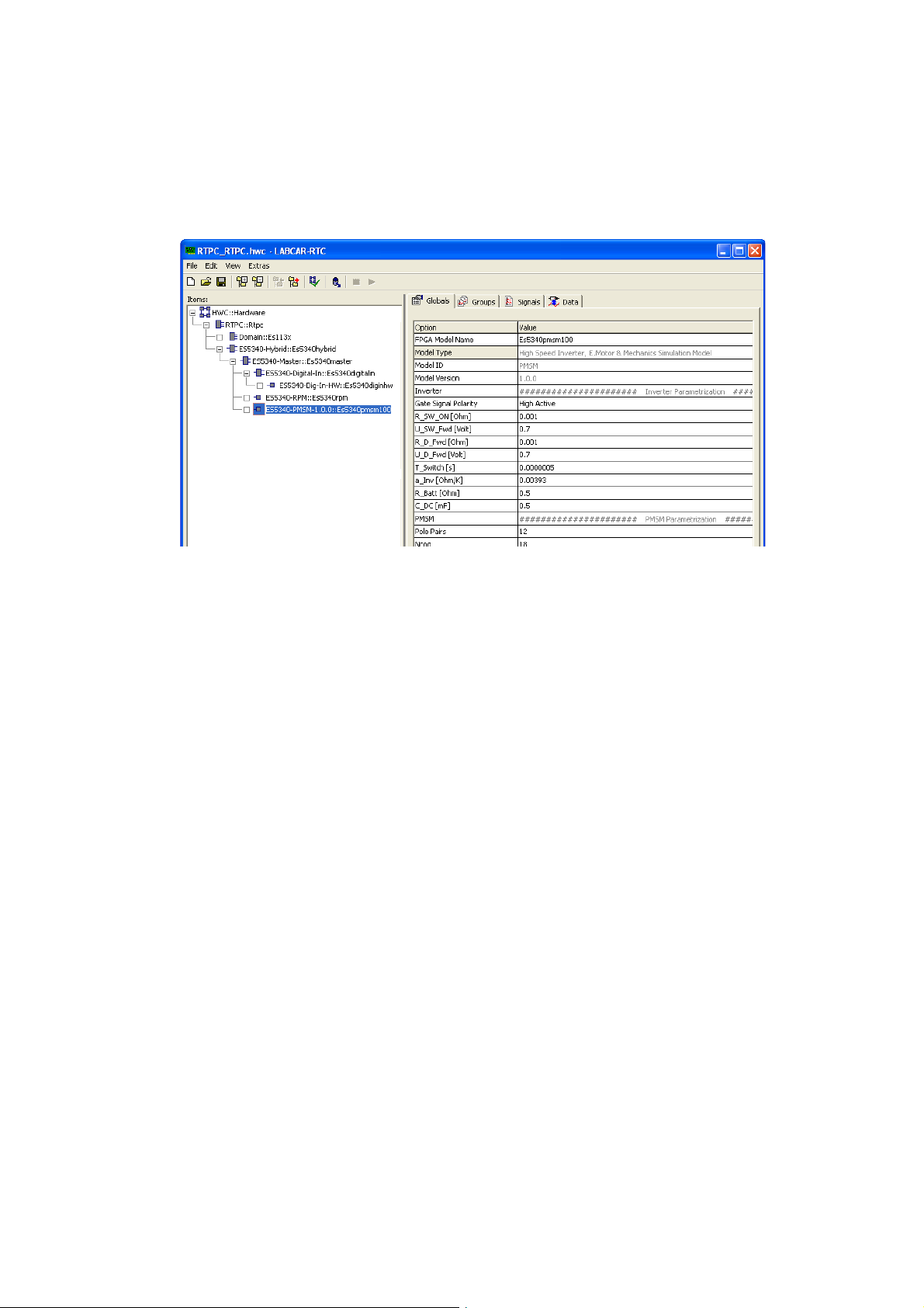
Configuring the Hardware in LABCAR-RTC ETAS
2. From the list, select the "ES5340-PMSM-X.X.X"
item and click OK.
The item is added.
ES5340.2 Electric Drive Simulation Board - User’s Guide72
Page 73
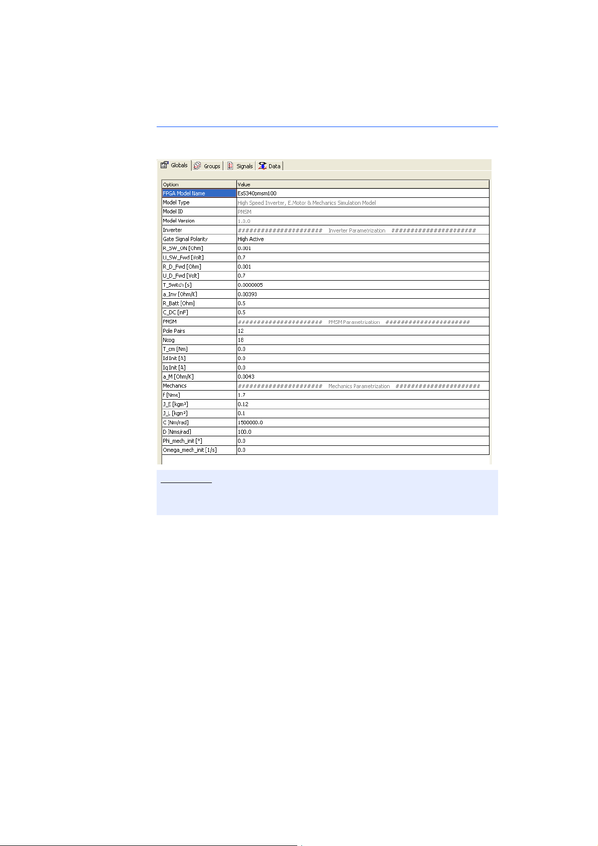
ETAS Configuring the Hardware in LABCAR-RTC
Note
Configuring the Model Parameters
The model is configured in the "Globals" tab and is divided into three model
components: "Inverter", "PMSM" and "Mechanics".
For a detailed description of the model variables, refer to the chapter on "FPGA
Models" on page 49,
ES5340.2 Electric Drive Simulation Board - User’s Guide 73
Page 74
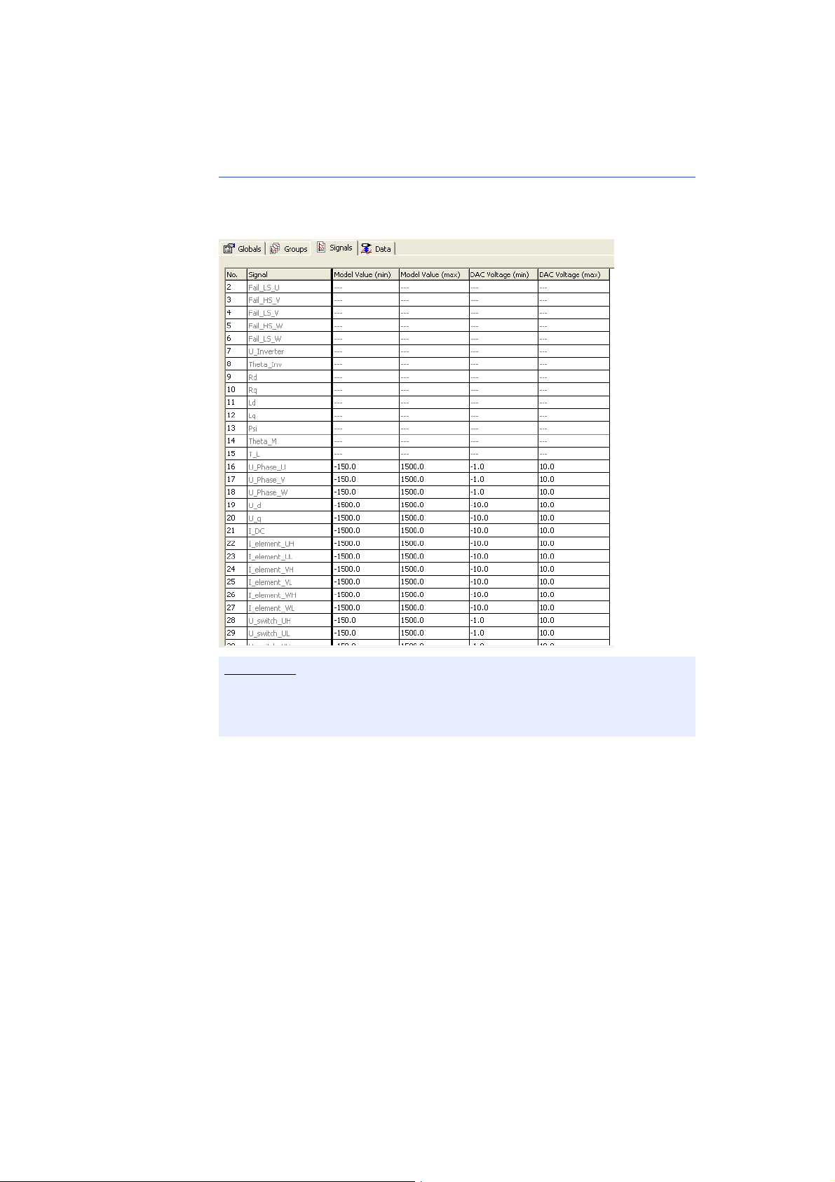
Configuring the Hardware in LABCAR-RTC ETAS
Note
Configuring the Value Ranges
The valid value ranges for the model variables are configured in the "Signals"
tab. Adapt the mapping between the physical and electrical variables according
to your hardware.
Note that the values of "DAC Voltage (min)" and "DAC Voltage (max)" are
intended as absolute values that are not undershot/exceeded by the D/A converters of the hardware.
ES5340.2 Electric Drive Simulation Board - User’s Guide74
Page 75
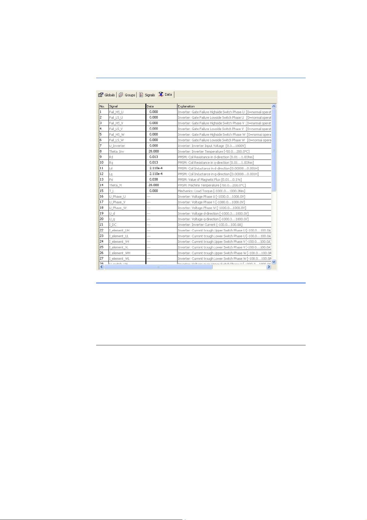
ETAS Configuring the Hardware in LABCAR-RTC
Determining Default Values
For certain model inputs, default values can be defined in the "Data" tab.
5.2.2 Software Model
If a model is run on the Real-Time PC, an item must be added for measurement
of the inverter gate signals from the ECU; in addition, a map of the current/
voltage values to the analog outputs must be created.
The duty cycles and the period of the PWM control signals are measured and
forwarded to the software model. The measurement itself can be synchronized
to an external signal or to the PWM period determined by clock recovery.
Configuring the Inverter Gate Measurement
1. Right-click the "ES5340-Digital-In" item and select
Add Item.
2. In the list, select the "ES5340-Dig-In-Inverter-Meas"
item and click OK.
The item is added.
ES5340.2 Electric Drive Simulation Board - User’s Guide 75
Page 76
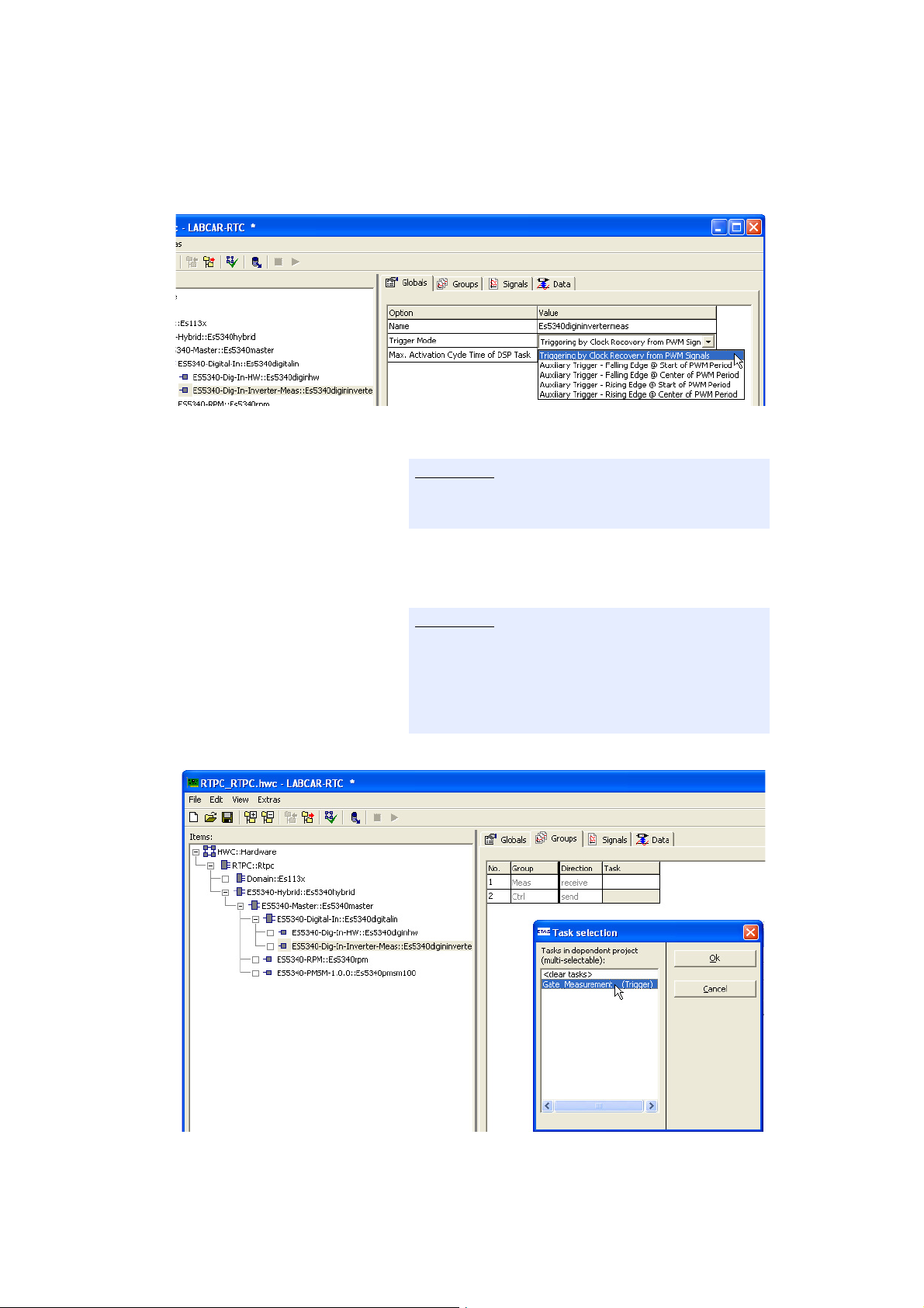
Configuring the Hardware in LABCAR-RTC ETAS
Note
Note
3. In the "Globals" tab, select the type of triggering to
be used for the measurement ("Trigger Mode").
4. Under "Nominal PWM Period Time...", enter the
period length of the PWM task of the ECU.
If you enter "0.0" here, the period of the "Receive"
task is applied as the period length here.
5. In the "Groups" tab, select the task to be activated
in the Real-Time PC after each period of the PWM
measurement.
For this purpose, a task of type "Trigger" must first
have been defined in the OS configuration of
LABCAR-IP in which the option "Exclusive Core
Usage" is enabled (see "“Exclusive Core Usage”
Mode" on page 28).
ES5340.2 Electric Drive Simulation Board - User’s Guide76
Page 77
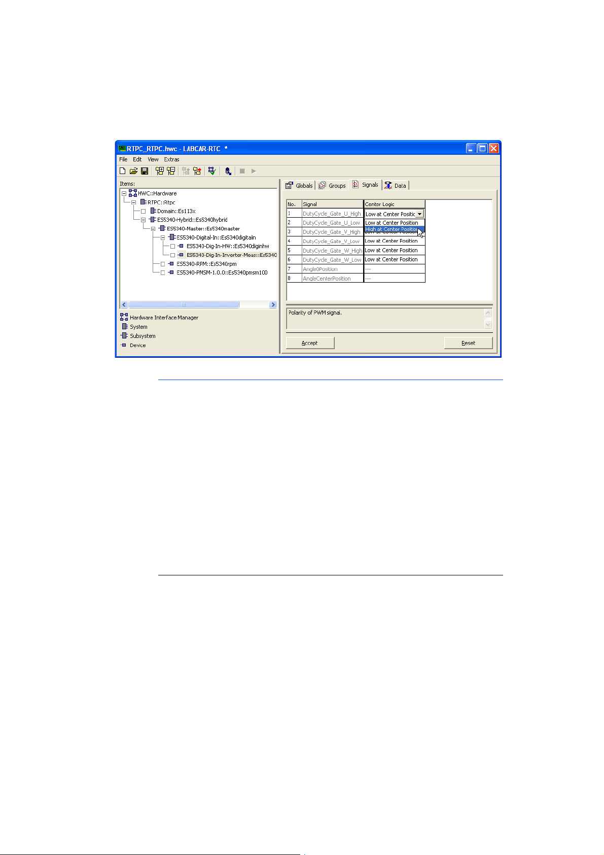
ETAS Configuring the Hardware in LABCAR-RTC
6. In the "Center Logic" column, configure the polarity of the gate signals.
Configuring Outputs for Current/Voltage Sensors
Output values of the model, such as alternating currents or direct currents/voltages, can be output synchronously to the PWM period using analog outputs.
For this purpose, two options exist:
• Direct output
The values of the model are converted from physical to electrical values
and enabled on the D/A converter on the ES5340.2.
• Predicted output
Only the amplitude and phase of the AC signal are taken over from the
model; the resulting sine wave, on the other hand, is generated in the
hardware. This results in much faster updating of the values for the D/A
converter output with smaller step sizes for model calculation.
Adding Analog Outputs ("Direct out")
1. Right-click the "ES5340-Master" item and select
Add Item.
2. In the list, select the "ES5340-Analog-Out" item
and click OK.
The item is added.
ES5340.2 Electric Drive Simulation Board - User’s Guide 77
Page 78
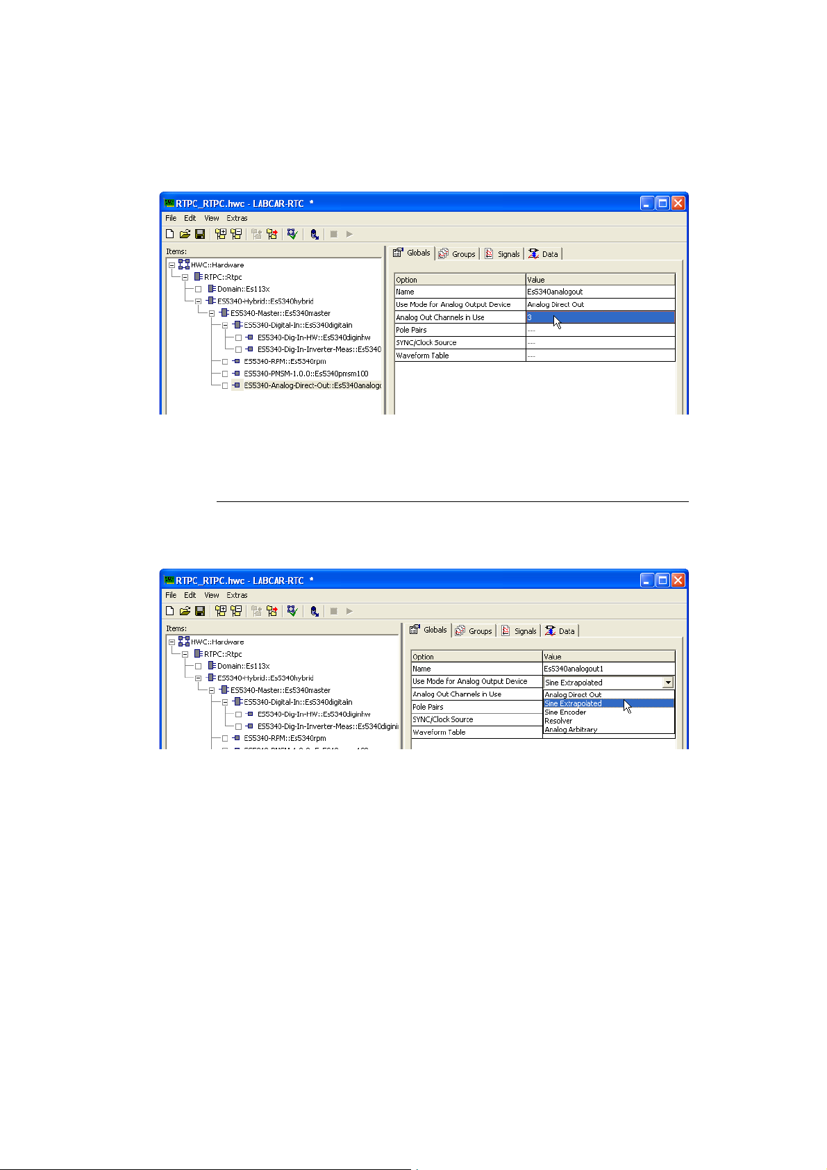
Configuring the Hardware in LABCAR-RTC ETAS
3. Leave the operating mode set to "Analog Direct
Out" and select the number of desired outputs.
For an additional configuration of this item, refer to the section on "Analog Outputs" on page 84.
Adding Analog Outputs (for Predicted Values)
1. Insert an "ES5340-Analog-Out" item as described
above.
2. For the operating mode, select "Sine Extrapolated".
3. Enter the desired number of outputs of this type.
4. Make sure that the correct number for the pole
pairs is specified.
ES5340.2 Electric Drive Simulation Board - User’s Guide78
Page 79
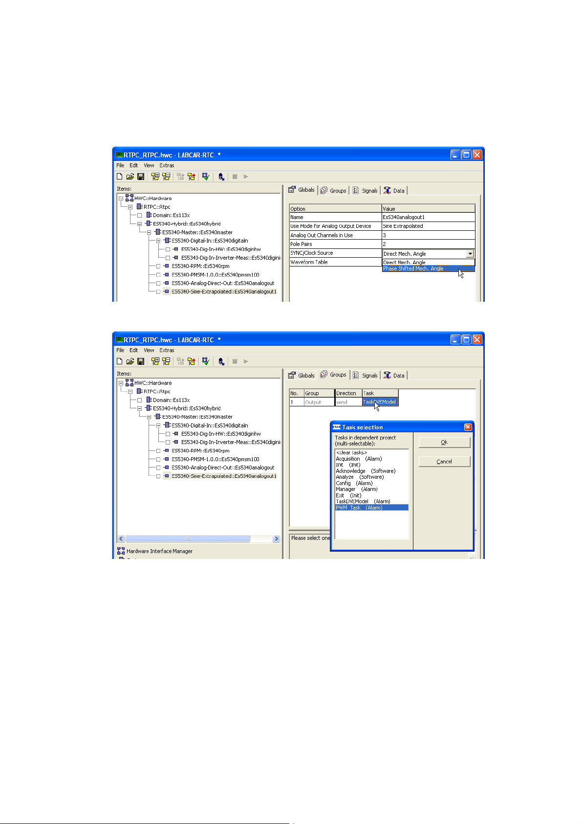
ETAS Configuring the Hardware in LABCAR-RTC
5. So that the phases of the signals can still be
changed later, for the option "Clock Source", select
the setting "Phase Shifted Mech. Angle".
6. To enable synchronized hardware access, change
the task in the "Groups" tab.
ES5340.2 Electric Drive Simulation Board - User’s Guide 79
Page 80
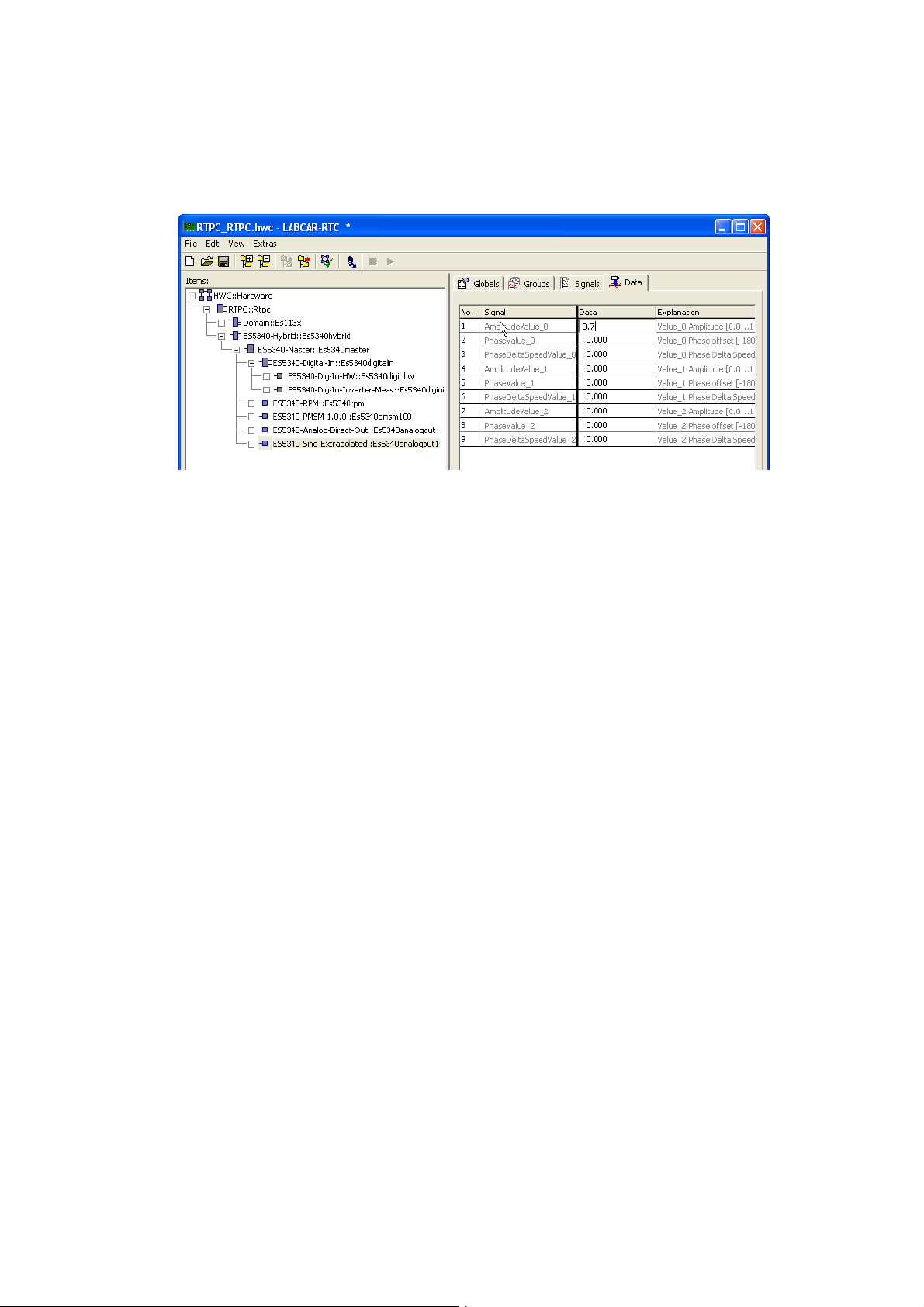
Configuring the Hardware in LABCAR-RTC ETAS
7. Finally, you can configure default values for the
amplitude and phase in the "Data" tab.
ES5340.2 Electric Drive Simulation Board - User’s Guide80
Page 81

ETAS Configuring the Hardware in LABCAR-RTC
5.3 I/O Configuration
This chapter provides a description of the configuration of the input and output
channels of the ES5340.2.
Specifically, it includes information about:
• "Adding an Analog Position Sensor" on page 81
• "Adding a Digital Position Sensor" on page 82
• "Adding Outputs of Type "Direct Analog Out"" on page 84
• "Adding Outputs of Type "Analog Arbitrary"" on page 85
• "Adding Outputs of Type "Direct Digital Out"" on page 86
• "Adding Outputs of Type "Digital Arbitrary"" on page 88
• "Adding an Analog Input" on page 89
• "Adding a Digital Input" on page 90
• "Configuring the signal sources of the analog multiplexer" on page 92
• "Configuring the voltage reference and output type" on page 93
• "Defining the Default Values" on page 94
• "Configuring the Signal Sources of the Digital Multiplexer" on page 94
• "Configuring the output mode" on page 95
• "Defining the Default Values" on page 96
• "Exiting LABCAR-RTC" on page 96
5.3.1 Position sensors
To generate position information for the ECU, specific items must be added to
the hardware configuration.
There are two types of position sensors:
• Analog sensors
Example of these include resolvers and sine encoders
• Digital sensors
An example of a digital sensor is the "Trixy" sensor in BOSCH ECUs.
Adding an Analog Position Sensor
1. Right-click the "ES5340-Master" item and select
Add Item.
2. In the list, select the "ES5340-Analog-Out" item
and click OK.
The item is added.
3. Select "Resolver" or "Sine Encoder" operating
mode
ES5340.2 Electric Drive Simulation Board - User’s Guide 81
Page 82
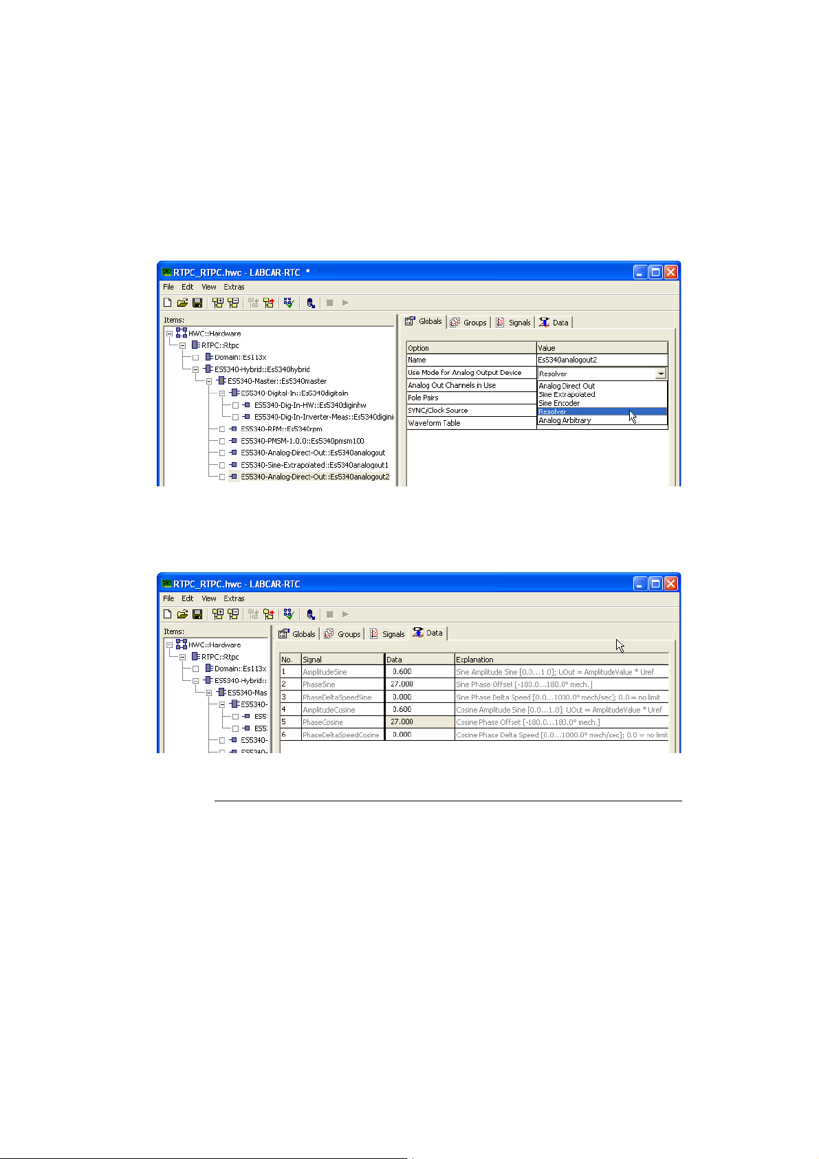
Configuring the Hardware in LABCAR-RTC ETAS
– The "Resolver" sensor type uses an external
excitation signal and returns a differential output signal (refer also to "Configuring the voltage reference and output type" on page 93).
– The type "Sine Encoder" does not need an exci-
tation signal and has a single-ended output.
4. Define the number of pole pairs.
5. For "SYNC/Clock Source", select the setting "Direct
Mech. Angle."
6. Define default values (in the "Data" tab).
Adding a Digital Position Sensor
1. Right-click the "ES5340-Master" item and select
Add Item.
2. In the list, select the "ES5340-Digital-Out" item and
click OK.
The item is added.
ES5340.2 Electric Drive Simulation Board - User’s Guide82
Page 83
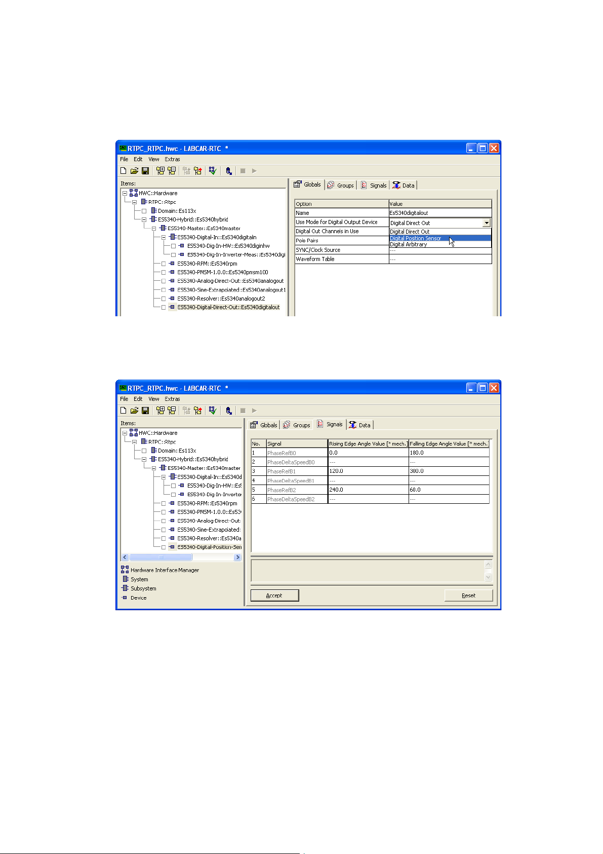
ETAS Configuring the Hardware in LABCAR-RTC
3. As the operating mode, select "Digital Position
Sensor".
4. Define the number of pole pairs.
5. For "SYNC/Clock Source", select the setting "Direct
Mech. Angle."
6. Configure the signal type (in the "Signals" tab).
ES5340.2 Electric Drive Simulation Board - User’s Guide 83
Page 84
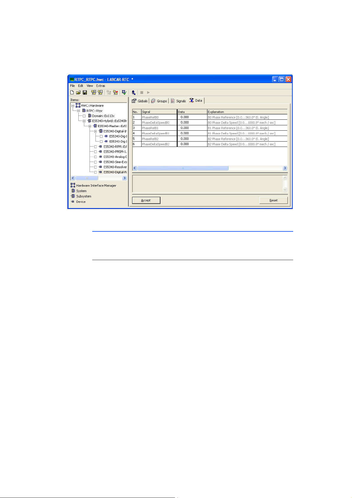
Configuring the Hardware in LABCAR-RTC ETAS
7. Define default values (in the "Data" tab).
5.3.2 Analog Outputs
These outputs are used to output analog values from a model to the A/D converters of the ECU.
Adding Outputs of Type "Direct Analog Out"
1. Right-click the "ES5340-Master" item and select
Add Item.
2. In the list, select the "ES5340-Analog-Out" item
and click OK.
The item is added.
3. Leave the option "Use Mode for Analog Output
Device" in the default setting, "Analog Direct Out".
ES5340.2 Electric Drive Simulation Board - User’s Guide84
Page 85
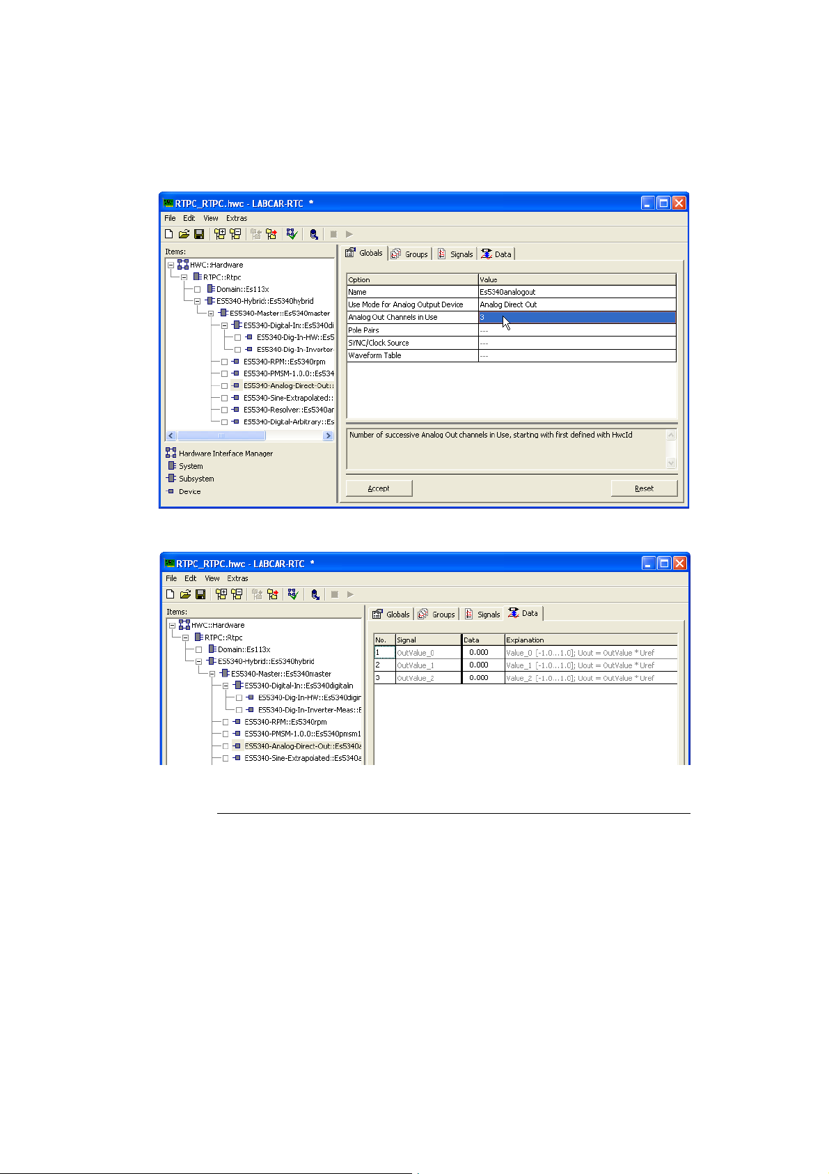
ETAS Configuring the Hardware in LABCAR-RTC
4. To configure multiple analog outputs in this item,
select the desired number in the "Globals" tab.
5. Select the "Data" tab to configure default values
for the outputs.
Adding Outputs of Type "Analog Arbitrary"
Outputs for arbitrary signals can be used to output user-defined signal patterns
(based on the current angle of the simulated electric motor).
This signal pattern can be used, for example, to simulate specific position sensors
and other variables with a direct relationship to the motor angle.
1. Right-click the "ES5340-Master" item and select
Add Item.
2. In the list, select the "ES5340-Analog-Out" item
and click OK.
The item is added.
ES5340.2 Electric Drive Simulation Board - User’s Guide 85
Page 86
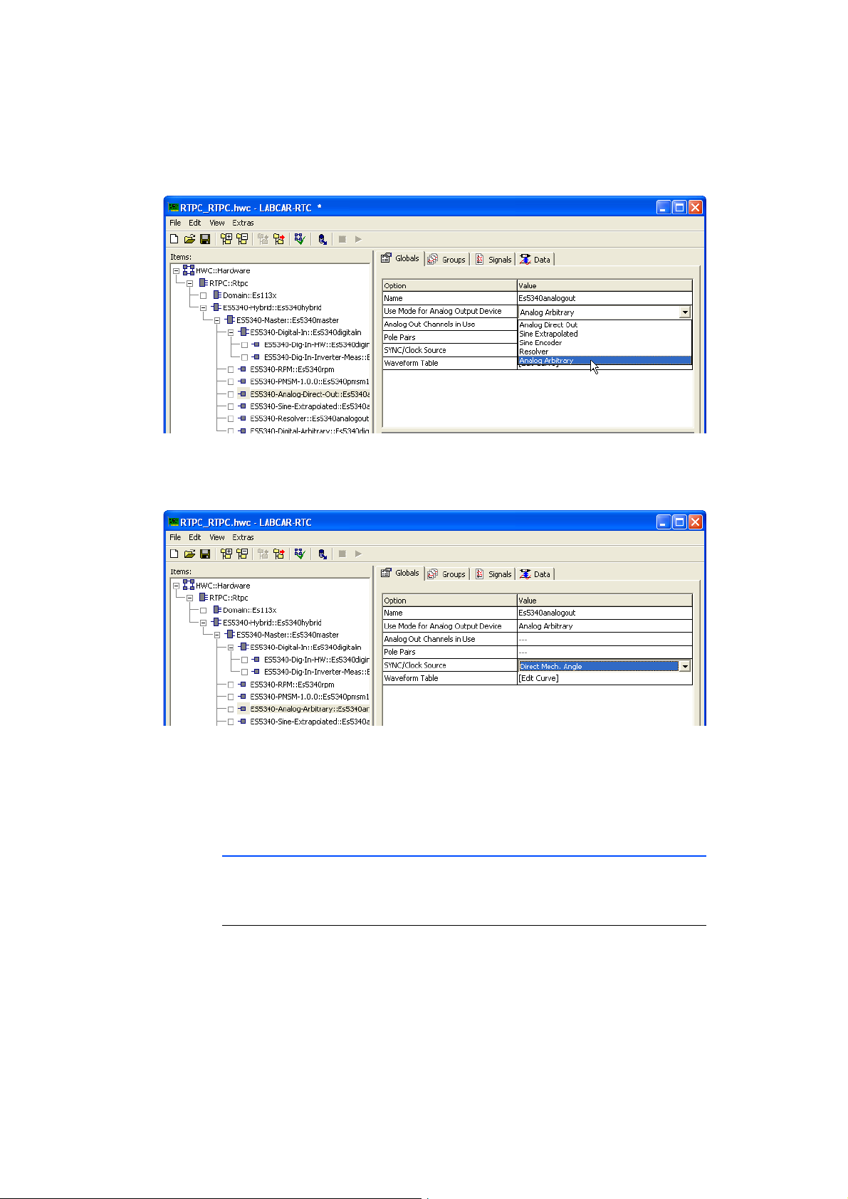
Configuring the Hardware in LABCAR-RTC ETAS
3. For the option "Use Mode for Analog Output
Device", select the "Analog Arbitrary" setting.
4. With the option "SYNC/Clock Source", the output
can be synchronized to the current motor angle or
a phase-shifted angle (e.g. for predicting current
values) can be used.
5.3.3 Digital Outputs
These outputs enable you to directly stimulate ECU inputs using values from the
model.
Adding Outputs of Type "Direct Digital Out"
5. With the "WaveformTable" option, you can edit the
desired output in the form of a table.
6. Select the "Data" tab to configure default values
for the outputs.
1. Right-click the "ES5340-Master" item and select
Add Item.
2. In the list, select the "ES5340-Digital-Out" item and
click OK.
The item is added.
ES5340.2 Electric Drive Simulation Board - User’s Guide86
Page 87
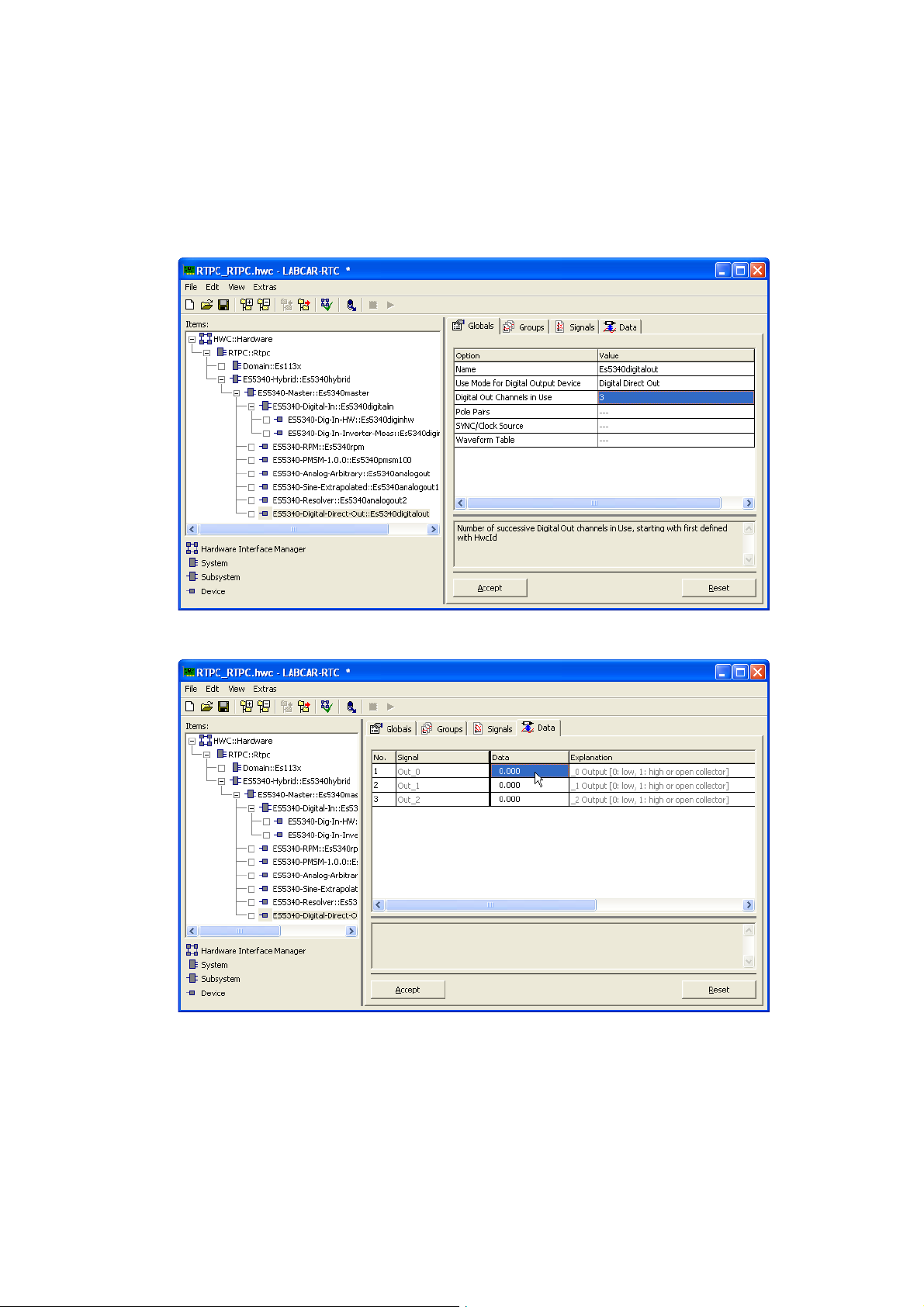
ETAS Configuring the Hardware in LABCAR-RTC
3. Leave the option "Use Mode for Digital Output
Device" in the default setting, "Digital Direct Out".
4. To configure multiple digital outputs in this item,
select the desired number in the "Globals" tab.
5. Select the "Data" tab to configure default values
for the outputs.
ES5340.2 Electric Drive Simulation Board - User’s Guide 87
Page 88
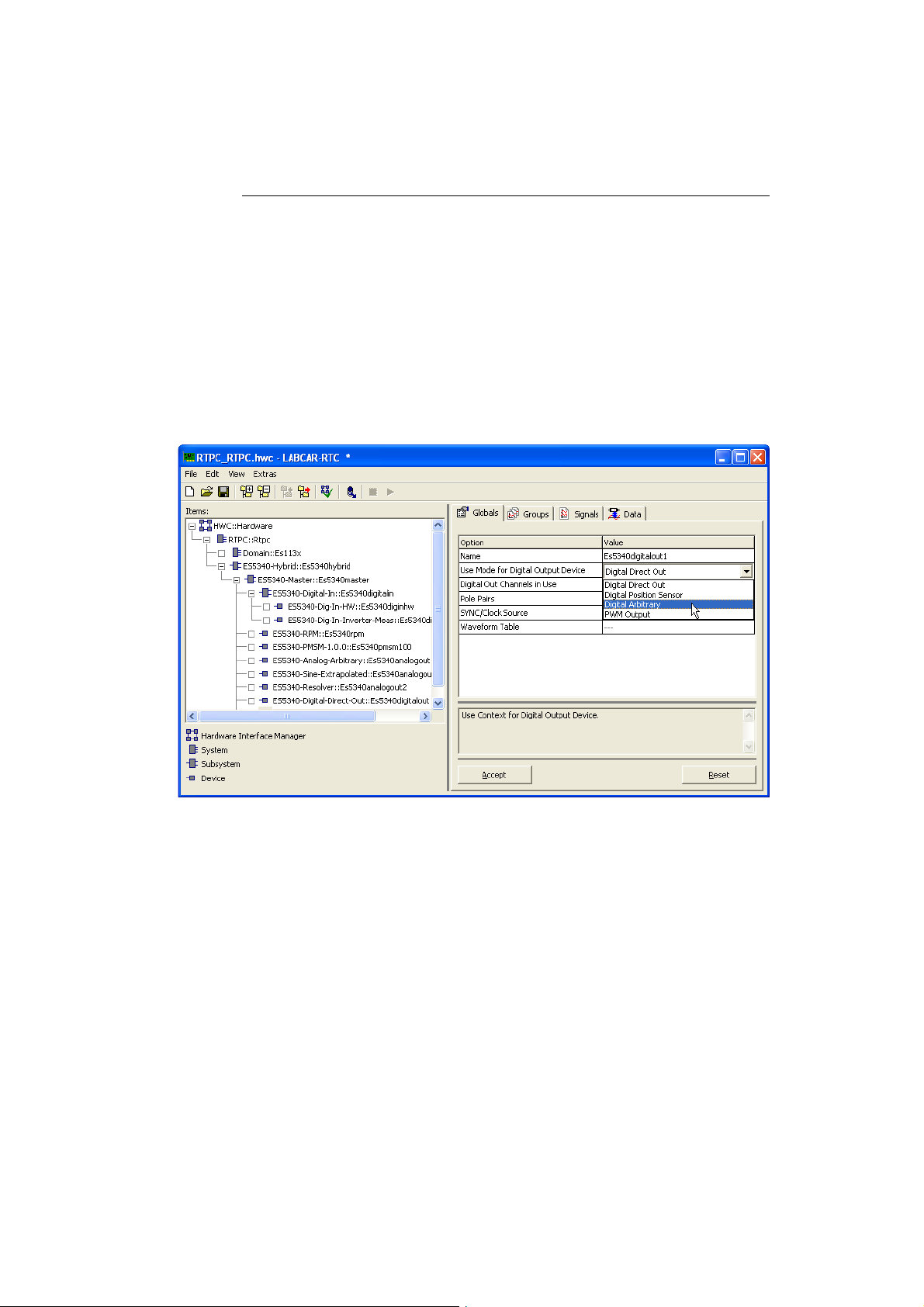
Configuring the Hardware in LABCAR-RTC ETAS
Adding Outputs of Type "Digital Arbitrary"
Outputs for arbitrary digital signals can be used to output user-defined signal
patterns (based on the current angle of the simulated electric motor).
This signal pattern can be used, for example, to simulate specific position sensors
and other variables with a direct relationship to the motor angle.
1. Right-click the "ES5340-Master" item and select
Add Item.
2. In the list, select the "ES5340-Digital-Out" item and
click OK.
The item is added.
3. For the option "Use Mode for Digital Output
Device", select the "Digital Arbitrary" setting.
ES5340.2 Electric Drive Simulation Board - User’s Guide88
Page 89
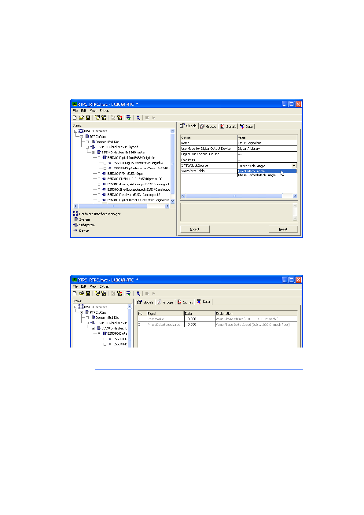
ETAS Configuring the Hardware in LABCAR-RTC
4. With the option "SYNC/Clock Source", the output
can be synchronized to the current motor angle or
a phase-shifted angle (e.g. for predicting current
values) can be used.
5.3.4 Analog Inputs
The four analog inputs of the ES5340.2 can be used to measure analog signals
from the ECU.
Adding an Analog Input
5. With the "WaveformTable" option, you can edit the
desired output in the form of a table.
6. Select the "Data" tab to configure default values
for the outputs.
1. Right-click the "ES5340-Master" item and select
Add Item.
2. In the list, select the "ES5340-Analog-In" item and
click OK.
The item is added.
ES5340.2 Electric Drive Simulation Board - User’s Guide 89
Page 90
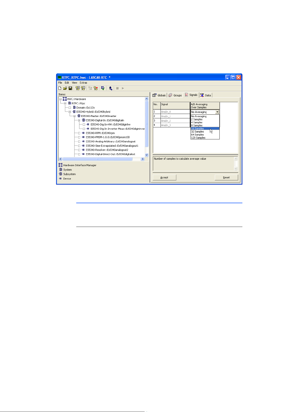
Configuring the Hardware in LABCAR-RTC ETAS
3. Select the "Signals" tab to, if necessary, calculate
an average of a configurable number of measured
values.
5.3.5 Digital Inputs
The digital inputs can be used to measure various properties of digital signals
(frequencies, duty cycles etc.).
Adding a Digital Input
1. Right-click the "ES5340-Dig-In" item and select
Add Item.
2. In the list, select the "ES5340-Dig-In-Meas" item
and click OK.
The item is added.
ES5340.2 Electric Drive Simulation Board - User’s Guide90
Page 91
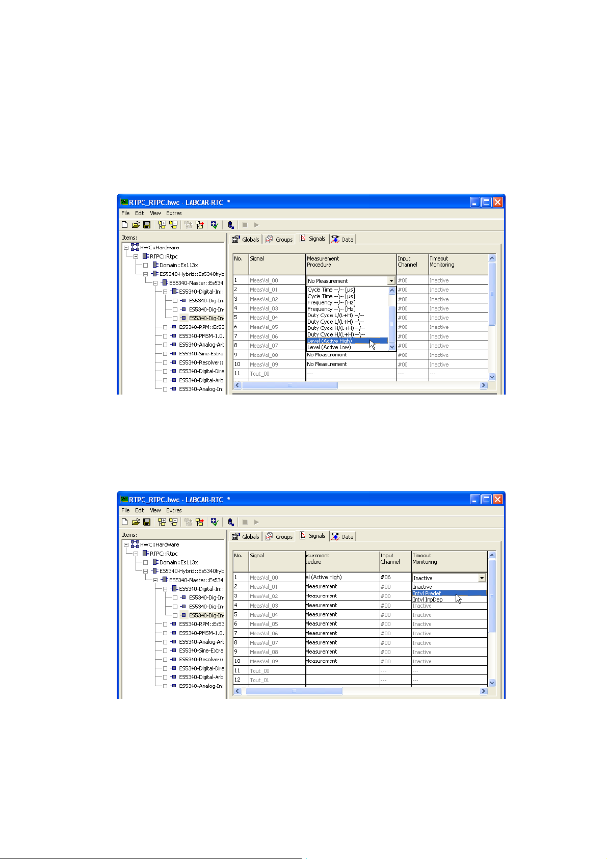
ETAS Configuring the Hardware in LABCAR-RTC
3. To configure the measurement, select the "Signals"
tab.
You can configure the measurement method in the
"Measurement Procedure" column. For a digital
input channel, multiple measurements can be carried out.
For each "ES5340-Dig-In-Meas" item, ten measurements are possible – if more measurements are
needed, additional items of the type "ES5340-DigIn-Meas" can be added.
4. For edge-based measurements, enable timeout
monitoring to ensure a corresponding response to
missing edges in the signal.
ES5340.2 Electric Drive Simulation Board - User’s Guide 91
Page 92
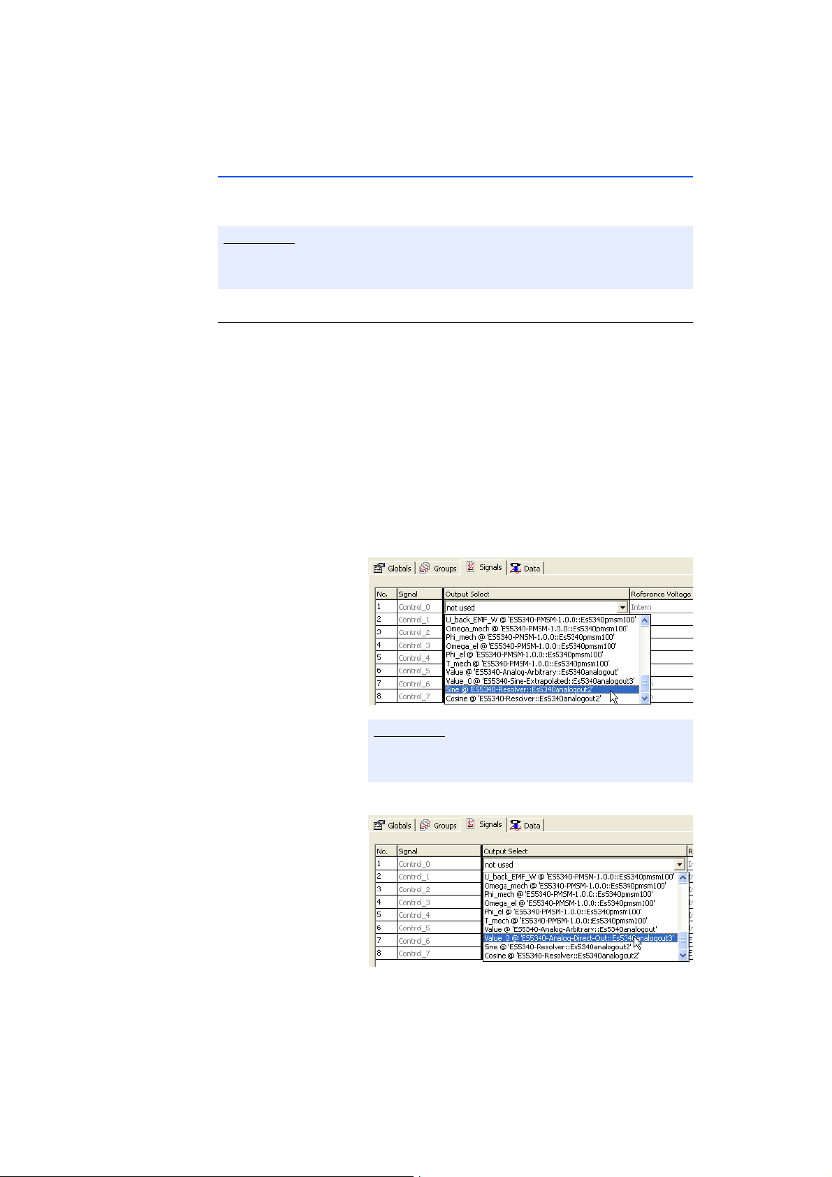
Configuring the Hardware in LABCAR-RTC ETAS
Note
Note
5.3.6 Signal Output via the Analog Multiplexer
Finally, you have to assign the defined logical signal sources to pins of the physical outputs on the ES5340.2.
For each "ES5340-Master" item, only one output multiplexer can be configured.
Configuring the signal sources of the analog multiplexer
1. Right-click the "ES5340-Master" item and select
Add Item.
2. In the list, select the "ES5340-Analog-Out-Mux"
item and click OK.
The item is added.
3. Switch to the "Signals" tab.
In the "Output Select" column, you can now define
a signal source for each of the eight output pins.
4. To do so, click the corresponding cell in the table.
The following signal sources are available:
– Analog position sensors:
Position sensors of type "Resolver" can be assigned to
outputs 6 and 7 only.
– Direct analog output (Analog-Direct-Out):
ES5340.2 Electric Drive Simulation Board - User’s Guide92
Page 93
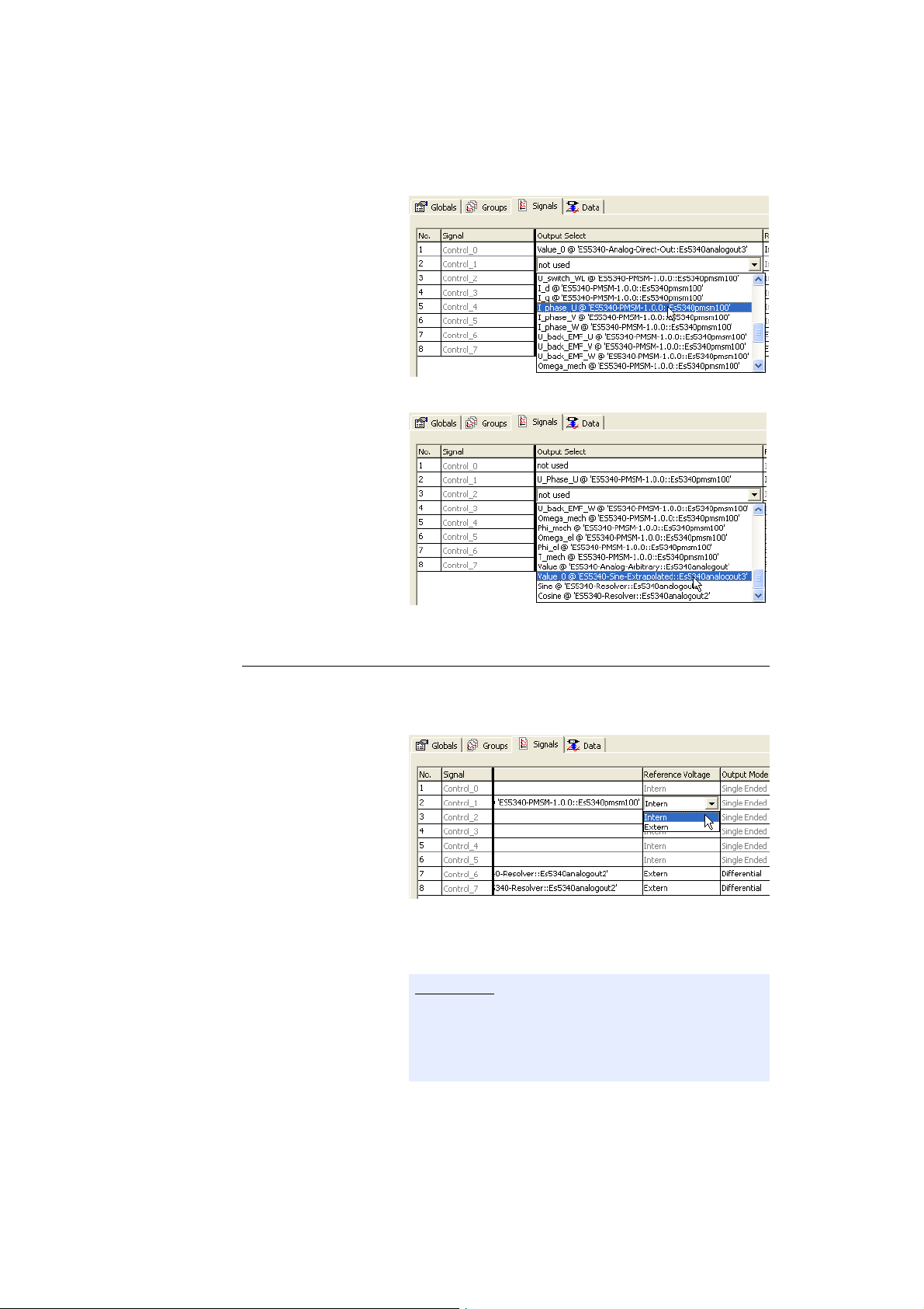
ETAS Configuring the Hardware in LABCAR-RTC
Note
– Analog output values from the FPGA model:
– Predicted analog outputs:
Configuring the voltage reference and output type
1. In the "Reference Voltage" column, select whether
the internal reference voltage or an external reference voltage is to be used.
2. In the "Output Mode" column, select whether the
signal is to be configured as "single-ended" or "differential".
Position sensors of the type "Resolver" can be
assigned to outputs 6 and 7 only – for these, an
external reference and differential output are configured automatically.
ES5340.2 Electric Drive Simulation Board - User’s Guide 93
Page 94
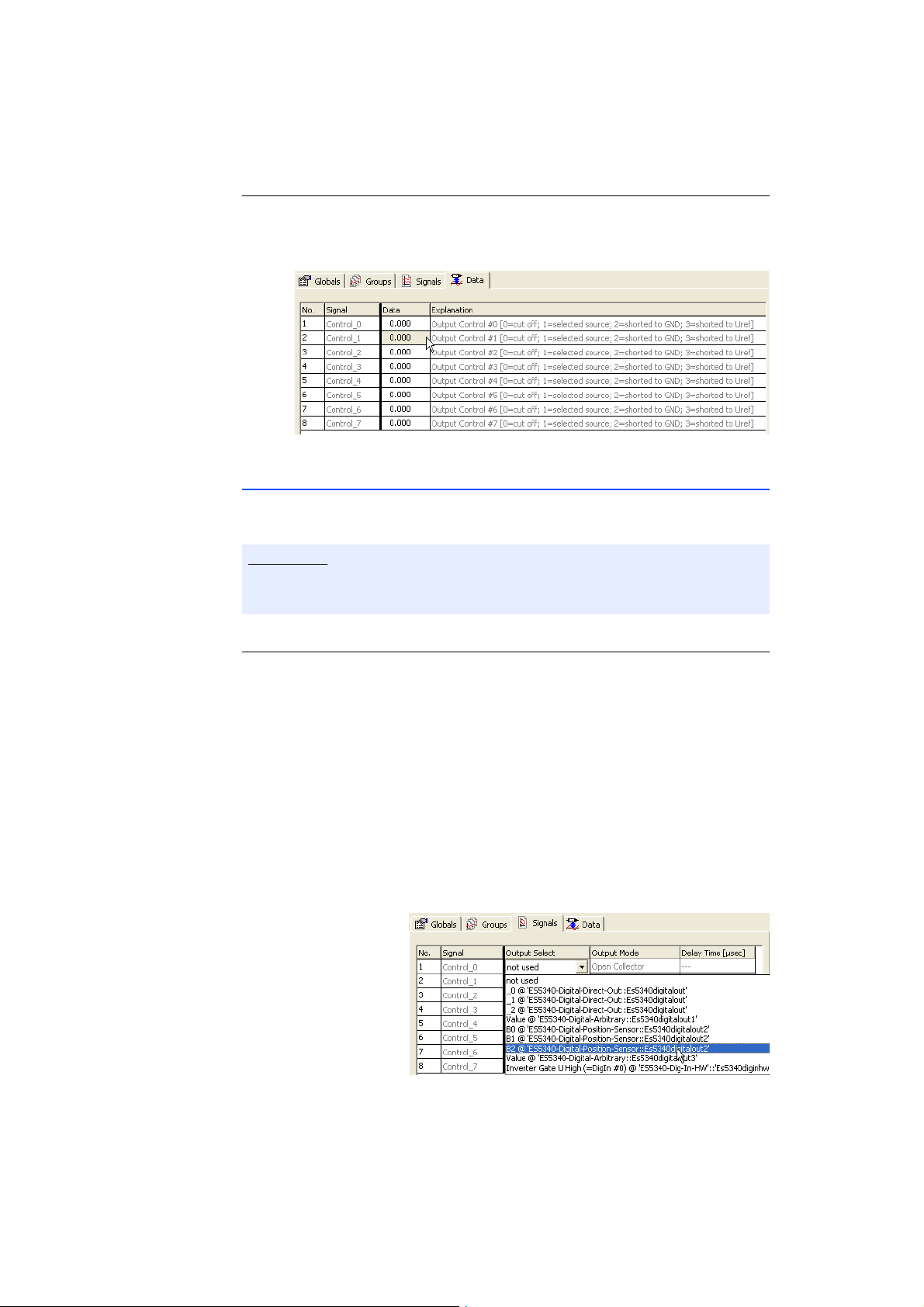
Configuring the Hardware in LABCAR-RTC ETAS
Note
Defining the Default Values
1. Select the "Data" tab to configure default values
for the outputs.
Four different settings exist for the output control:
5.3.7 Signal Output via the Digital Multiplexer
For output of the digital signals, an item must be defined for a digital output
multiplexer.
For each "ES5340-Master" item, only one digital multiplexer can be configured.
Configuring the Signal Sources of the Digital Multiplexer
1. Right-click the "ES5340-Master" item and select
Add Item.
2. In the list, select the "ES5340-Digital-Out-Mux"
item and click OK.
The item is added.
3. Switch to the "Signals" tab.
In the "Output Select" column, you can now define
a signal source for each of the eight output pins.
4. To do so, click the corresponding cell in the table.
The following signal sources are available:
– Digital position sensors
ES5340.2 Electric Drive Simulation Board - User’s Guide94
Page 95
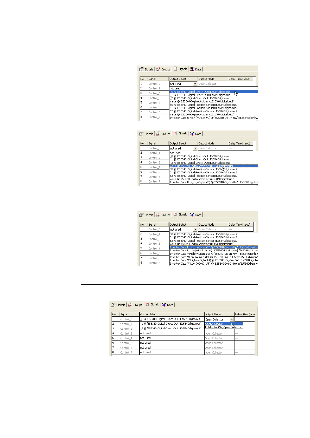
ETAS Configuring the Hardware in LABCAR-RTC
– Direct digital output (Digital-Direct-Out):
– Digital arbitrary signals (Digital-Arbitrary):
– Feedback of the inverter gate signals
Configuring the output mode
1. Select the desired output mode ("Open Collector"
or "Pull-Up to +5 V").
The PWM signals can be fed back for diagnostic
purposes (with a configurable delay).
ES5340.2 Electric Drive Simulation Board - User’s Guide 95
Page 96
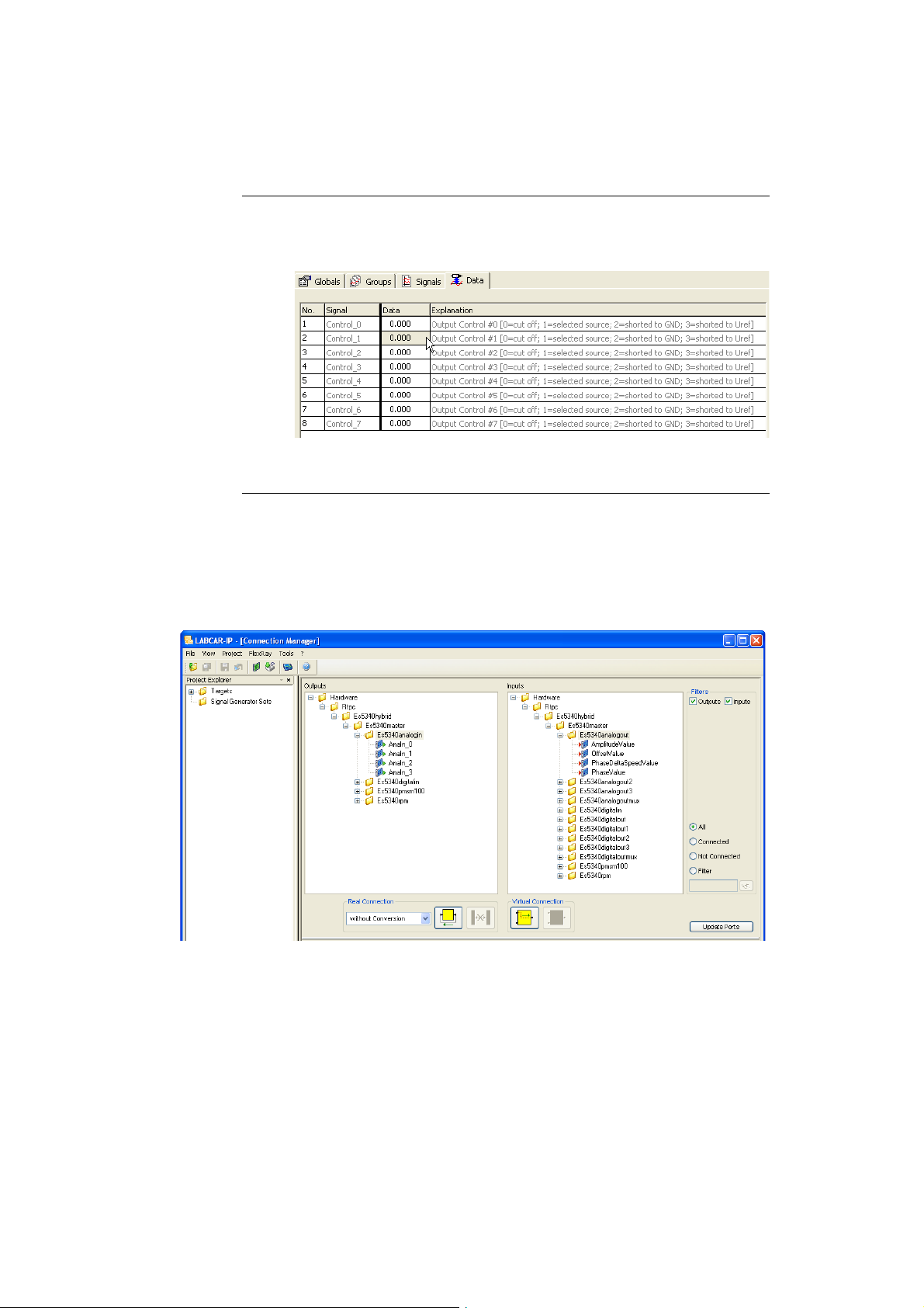
Configuring the Hardware in LABCAR-RTC ETAS
Defining the Default Values
1. Select the "Data" tab to configure default values
for the outputs.
2. Four different settings exist for the output control:
Exiting LABCAR-RTC
1. Save the settings with File → Save.
2. In LABCAR-IP, start the code generation (Project →
Build).
The inputs and outputs of the hardware (and of the
FPGA model where applicable) are now available in
the Connection Manager.
ES5340.2 Electric Drive Simulation Board - User’s Guide96
Page 97

ETAS Connector Assignment and Display Elements
6 Connector Assignment and Display Elements
This chapter contains the description of the connectors and display elements of
the ES5340.2 Electric Drive Simulation Board. It consists of the following sections:
• "Connector Assignment" on page 98
Here, all connectors on the front panel are described.
– "Connectors for the Outputs (ES5340.2-M and ES5340.1-S)"
on page 98
– "Connectors for the Inputs (ES5340.2-M only)" on page 99
– "Connectors for the Angle Clock Signal (ES5340.2-M only)"
on page 101
• "Display Elements" on page 101
Here, the meaning of the LED display on the front panel is described.
ES5340.2 Electric Drive Simulation Board - User’s Guide 97
Page 98
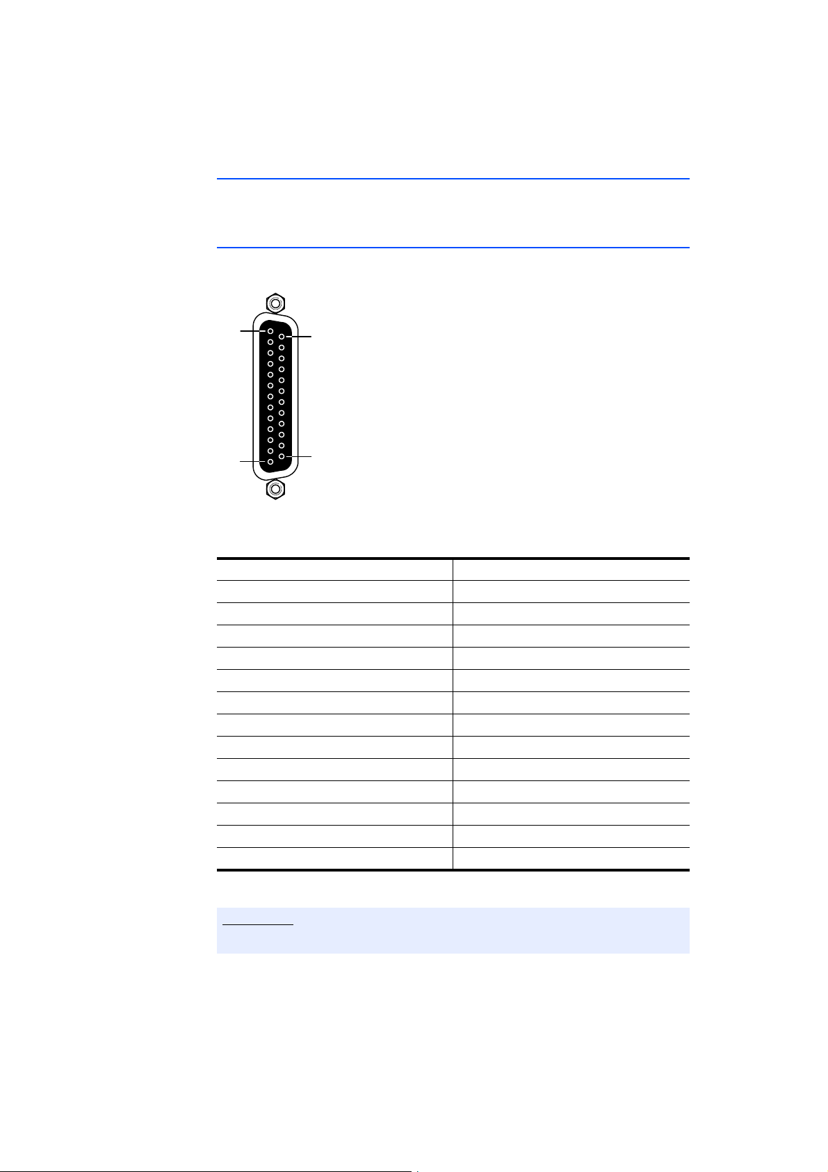
Connector Assignment and Display Elements ETAS
Note
13
25
14
1
6.1 Connector Assignment
This section describes the assignment of the connectors of the inputs and outputs of the ES5340.2.
6.1.1 Connectors for the Outputs (ES5340.2-M and ES5340.1-S)
The connector is a DSUB25 connector (female). The shielding is to the front panel
and housing potential and thus to protective earth.
Fig. 6-1 Connectors for the outputs (top view)
Pin Signal Pin Signal
1 Analog Output Channel 0 14 Ground Channel 0
2 External Ref. Channel 0 15 Digital Output Channel 0
3 Analog Output Channel 1 16 Ground Channel 1
4 External Ref. Channel 1 17 Digital Output Channel 1
5 Analog Output Channel 2 18 Ground Channel 2
6 External Ref. Channel 2 19 Digital Output Channel 2
7 Analog Output Channel 3 20 Ground Channel 3
8 External Ref. Channel 3 21 Digital Output Channel 3
9 Analog Output Channel 4 22 Ground Channel 4
10 External Ref. Channel 4 23 Digital Output Channel 4
11 Analog Output Channel 5 24 Ground Channel 5
12 External Ref. Channel 5 25 Digital Output Channel 5
13 n.c. Housing to protective earth
Tab. 6-1 Assignment of the connectors for the outputs
Analog and digital ground of an output channel are identical!
ES5340.2 Electric Drive Simulation Board - User’s Guide98
Page 99
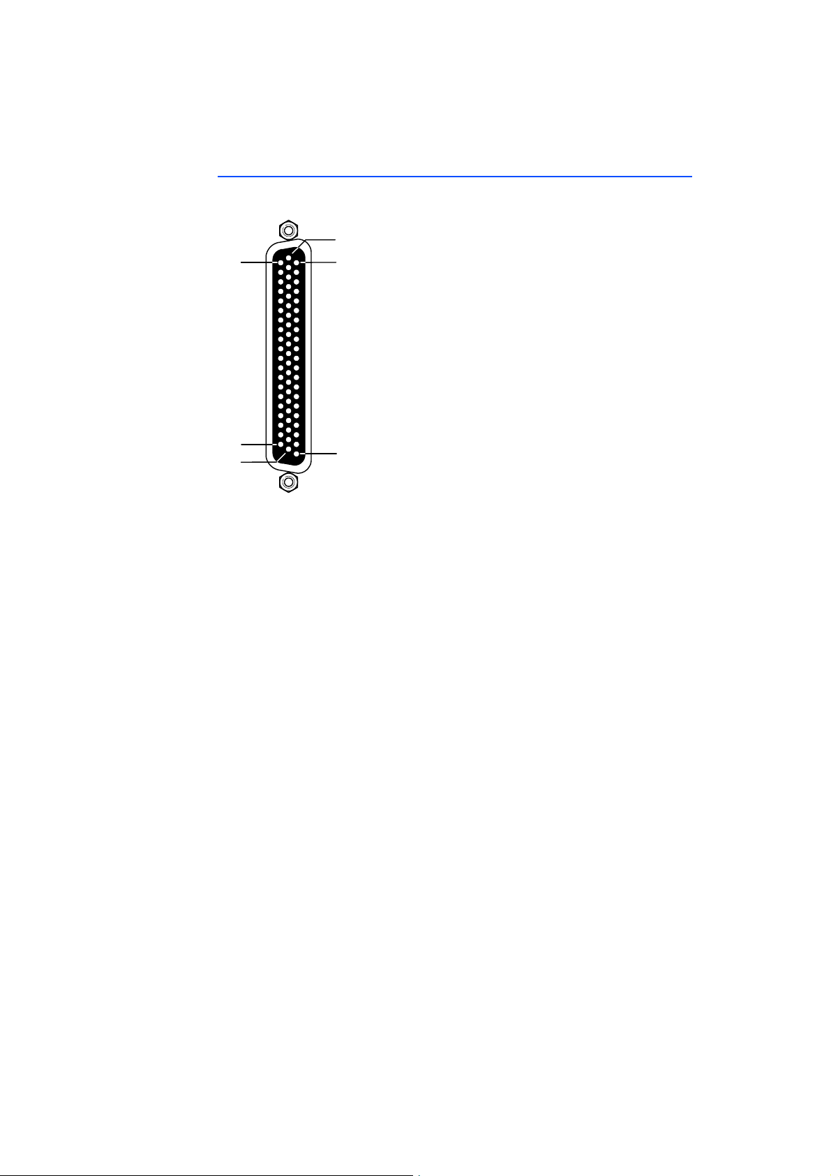
ETAS Connector Assignment and Display Elements
43
21
42
62
1
22
6.1.2 Connectors for the Inputs (ES5340.2-M only)
The connector is a DSUB62HD connector (male). The shielding is to protective
earth.
Fig. 6-2 Connectors for the inputs (top view)
ES5340.2 Electric Drive Simulation Board - User’s Guide 99
Page 100
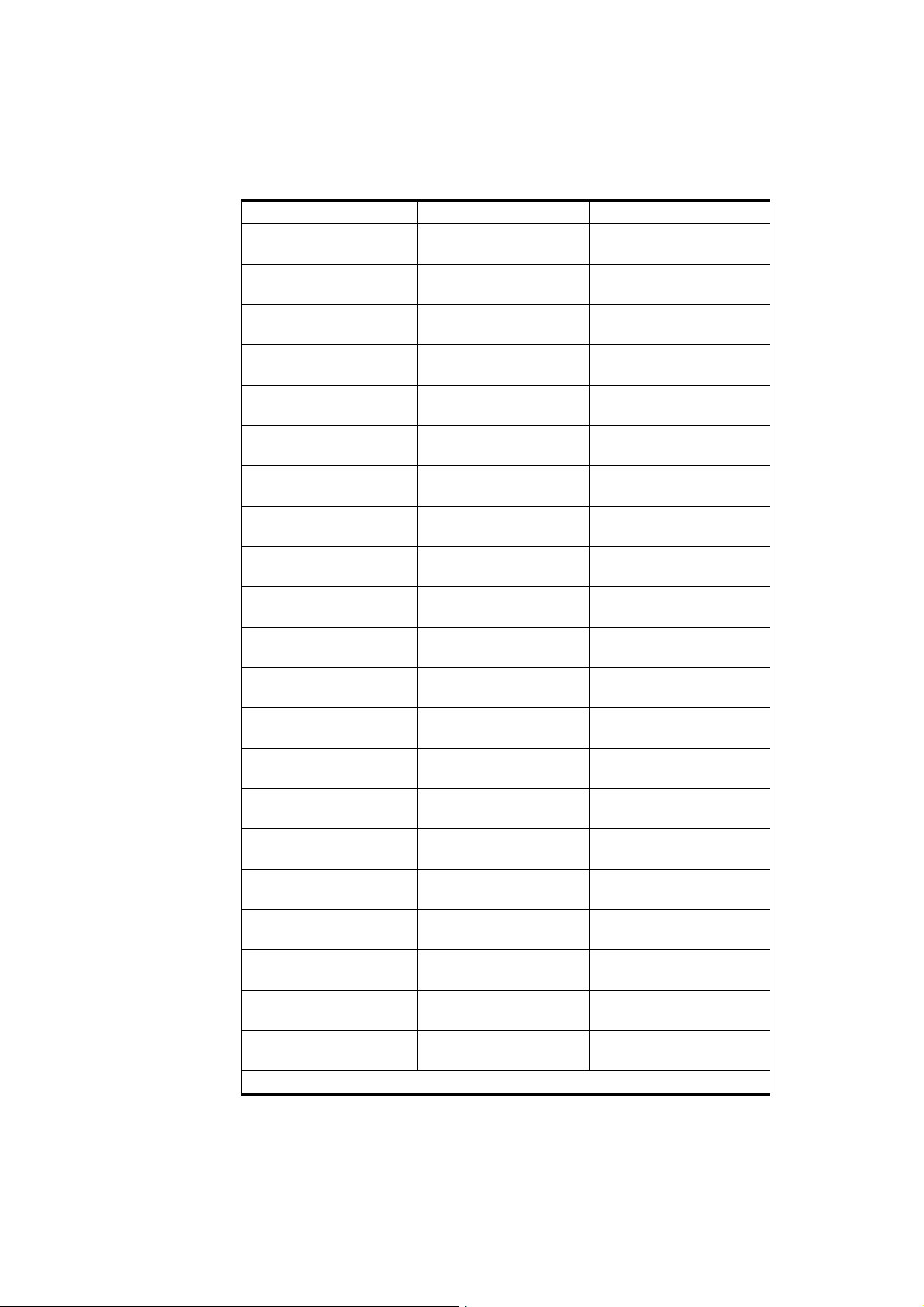
Connector Assignment and Display Elements ETAS
Pin Signal Pin Signal Pin Signal
1 Analog Output
Channel 6 –
2 Digital Output
Channel 6
3 Analog Output
Channel 7 –
4 Digital Output
Channel 7
5 Digital Input
Channel 0
6 Digital Input
Channel 1
7 Digital Input
Channel 2
8 Digital Input
Channel 3
9 Digital Input
Channel 4
10 Digital Input
Channel 5
11 Digital Input
Channel 6
12 Digital Input
Channel 7
13 Digital Input
Channel 8
14 Digital Input
Channel 9
15 Digital Input
Channel 10
16 Digital Input
Channel 11
17 Digital Input
Channel 12
18 Digital Input Ground 39 Analog Input
19 Analog Input
Channel 0
20 Analog Input
Channel 1
21 Analog Input
Ground
* See note on page 101!
22 Analog Output
Channel 6 +
23
Excitation + *
24 Analog Output
Channel 7 +
25
Excitation – *
26 Digital Input
Channel 13
27 Digital Input
Channel 14
28 Digital Input
Channel 15
29 Digital Input
Channel 16
30 Digital Input
Channel 17
31 Digital Input
Channel 18
32 Digital Input
Channel 19
33 Digital Input Ground 54 Digital Input Ground
34 Digital Input Ground 55 Digital Input Ground
35 Digital Input Ground 56 Digital Input Ground
36 Digital Input Ground 57 Digital Input Ground
37 Digital Input Ground 58 Digital Input Ground
38 Digital Input Ground 59 Digital Input Ground
Ground
40 Analog Input
Channel 2
41 Analog Input
Channel 3
42 Analog Input
Ground
43 Analog Output
Channel 6 AGND *
44 Digital Output
Channel 6 AGND *
45 Analog Output
Channel 7 AGND *
46 Digital Output
Channel 7 AGND *
47 Digital Input Ground
48 Digital Input Ground
49 Digital Input Ground
50 Digital Input Ground
51 Digital Input Ground
52 Digital Input Ground
53 Digital Input Ground
60 Analog Input Ground
61 Analog Input Ground
62 Analog Input Ground
Housing to protective earth
Tab. 6-2 Assignment of the connectors for the inputs
ES5340.2 Electric Drive Simulation Board - User’s Guide100
 Loading...