

Page 1

ES1392.1 High Current Switch Board
User’s Guide
Page 2

Copyright
The data in this document may not
notification from ETAS GmbH. ETAS GmbH undertakes no further obligation in
relation to this document. The software described in it can only be used if the
customer is in possession of a general license agreement or single license.
Using and copying is only allowed in concurrence with the specifications stipulated in the contract.
Under no circumstances may any part of this document be copied, reproduced, transmitted, stored in a retrieval system or translated into another language without the express written permission of ETAS GmbH.
© Copyright 2003-2018 ETAS GmbH, Stuttgart
The names and designations used in this document are trademarks or brands
belonging to the respective owners.
R02 EN -
ES1392.1 High Current Switch Board2
12.2018 TTN F 00K 102 735
be altered or amended without special
Page 3

Contents
1 Introduction . . . . . . . . . . . . . . . . . . . . . . . . . . . . . . . . . . . . . . . . . . . . . . . . . . . . . 5
1.1 Applications . . . . . . . . . . . . . . . . . . . . . . . . . . . . . . . . . . . . . . . . . . . . . . . 5
1.2 Features . . . . . . . . . . . . . . . . . . . . . . . . . . . . . . . . . . . . . . . . . . . . . . . . . . 6
1.3 Block Diagram . . . . . . . . . . . . . . . . . . . . . . . . . . . . . . . . . . . . . . . . . . . . . . 9
2 Hardware . . . . . . . . . . . . . . . . . . . . . . . . . . . . . . . . . . . . . . . . . . . . . . . . . . . . . . 11
2.1 Functional Description . . . . . . . . . . . . . . . . . . . . . . . . . . . . . . . . . . . . . . . 11
2.2 Configuring Battery Node 0 . . . . . . . . . . . . . . . . . . . . . . . . . . . . . . . . . . . 12
2.3 Controlling the Switches . . . . . . . . . . . . . . . . . . . . . . . . . . . . . . . . . . . . . 13
2.4 Overcurrent Protection with the Status Output . . . . . . . . . . . . . . . . . . . . 13
2.5 EEPROM . . . . . . . . . . . . . . . . . . . . . . . . . . . . . . . . . . . . . . . . . . . . . . . . . 13
2.6 Battery Voltage at the "CTRL" Connector . . . . . . . . . . . . . . . . . . . . . . . . 14
2.7 MRC Signal . . . . . . . . . . . . . . . . . . . . . . . . . . . . . . . . . . . . . . . . . . . . . . . 14
2.8 Reverse-Connect Protection of the Battery Node Switches . . . . . . . . . . . . 14
2.9 Parallel Switching of Several Battery Nodes . . . . . . . . . . . . . . . . . . . . . . . 15
2.10 Potential Difference between Ground and -UBatt . . . . . . . . . . . . . . . . . . 15
2.11 Battery Voltage at the "BATTERY NODES" Connector . . . . . . . . . . . . . . . 15
2.12 Protective Measures . . . . . . . . . . . . . . . . . . . . . . . . . . . . . . . . . . . . . . . . . 15
2.12.1 +UBatt and -UBatt at "BATTERY NODES" . . . . . . . . . . . . . . . . . 16
2.12.2 +UBatt and -UBatt at "CTRL". . . . . . . . . . . . . . . . . . . . . . . . . . 17
Contents 3
Page 4

2.12.3 MRC Signal between "BATTERY NODES" and "CTRL" . . . . . . . 17
2.12.4 Supply Voltages at "SUPPLY" . . . . . . . . . . . . . . . . . . . . . . . . . . 17
3 Pin Assignment. . . . . . . . . . . . . . . . . . . . . . . . . . . . . . . . . . . . . . . . . . . . . . . . . . 19
3.1 "BATTERY NODES" Connector . . . . . . . . . . . . . . . . . . . . . . . . . . . . . . . . 19
3.2 "BATTERY INPUT" Connector . . . . . . . . . . . . . . . . . . . . . . . . . . . . . . . . . 21
3.3 "CTRL" Connector . . . . . . . . . . . . . . . . . . . . . . . . . . . . . . . . . . . . . . . . . 21
3.4 "SUPPLY" Connector . . . . . . . . . . . . . . . . . . . . . . . . . . . . . . . . . . . . . . . . 22
4 Accessories. . . . . . . . . . . . . . . . . . . . . . . . . . . . . . . . . . . . . . . . . . . . . . . . . . . . . 25
4.1 Cables . . . . . . . . . . . . . . . . . . . . . . . . . . . . . . . . . . . . . . . . . . . . . . . . . . . 25
4.1.1 Cable CBAV300.1-2: Connection between ES1392.1 and Power
Supply (Battery Voltages) . . . . . . . . . . . . . . . . . . . . . . . . . . . . . 25
4.1.2 Cable CBV300.1-0.5: Connection between ES1391 and ES139226
5 Technical Data . . . . . . . . . . . . . . . . . . . . . . . . . . . . . . . . . . . . . . . . . . . . . . . . . . 29
6 ETAS Contact Addresses . . . . . . . . . . . . . . . . . . . . . . . . . . . . . . . . . . . . . . . . . . . 33
Contents4
Page 5

1Introduction
This section contains information about the basic features and applications of
the ES1392.1 High Current Switch Board. A block diagram is also included
here to show the schematic layout of the board.
note
Some components of the ES1392.1 High Current Switch Board may be damaged
or destroyed by electrostatic discharges. Please keep the board in its storage
package until it is installed.
The ES1392.1 High Current Switch Board should only be taken from its package,
configured and installed at a working place that is protected against static discharge.
note
The components, connectors and conductors of the ES1392.1 High Current
Switch Board may carry dangerous voltages.
These voltages may even exist when the ES1392.1 is not installed in the ES4100
or ES4300 or the ES4100 or ES4300 is powered off.
Make sure that the ES1392.1 is protected against contact during operation. Disconnect all connections to the ES1392.1 before removing the board.
1.1 Applications
The ES1392.1 High Current Switch Board is used to switch five high current
battery nodes to +UBatt (five nodes) or -UBatt (one node).
The ES1391.1 Power Supply Controller Board is used to control the ES1392.1
High Current Switch Board with TTL signals. An ES1391.1 Power Supply Controller Board can control up to two ES1392.1 High Current Switch Boards and
at the same time up to two battery voltage power supplies.
Five battery nodes can be switched per voltage when two ES1392.1 High Current Switch Boards and two power supplies (for example 12 V and 42 V) are
used.
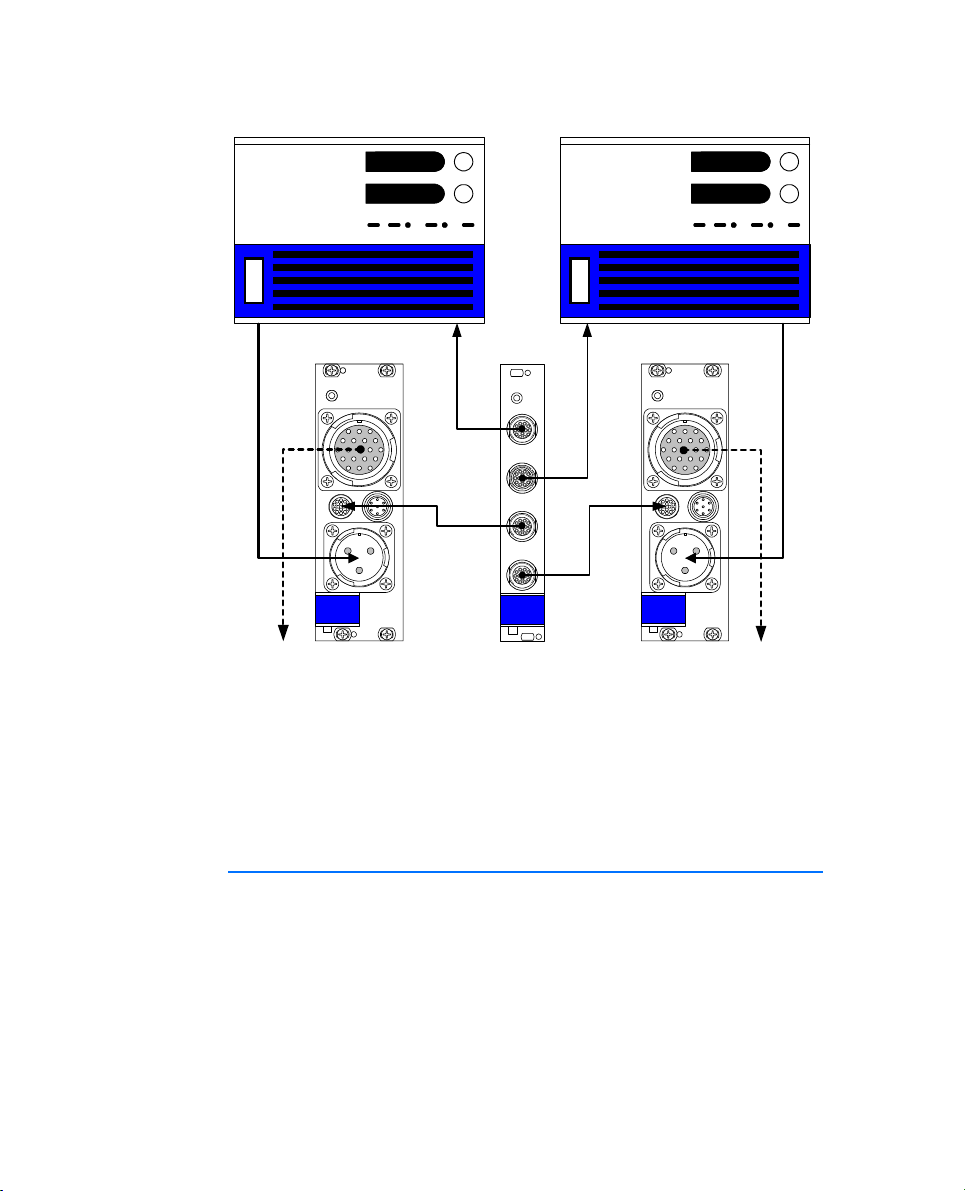
An example of this kind of scenario is shown in Fig. 1-1.
Introduction 5
Page 6
EX - 750L2
EXTENDED RANGE DC POWER SUPPLY
0-60V / 0-50A, 750W
8 8 8 8
8 8 8 8
8 8 8 8
VOLTAGE
V
V
CURRENT
A
OUTPUTOVPPRESET OCP
EX - 750L2
EXTENDED RANGE DC POWER SUP P L Y
0-60V / 0-50A, 750W
8 8 8 8
8 8 8 8
8 8 8 8
VOLTAGE
V
V
CURRENT
A
OUTPUTOVPPRESET OCP
I
O
UBatt 1
CBAV300.1-2
BATTERY
NODES
<
CTRL
SUPPLY
Switch 0-4
ES1392.1
BATTERY
INPUT
CBV300.1-0.5
PWR-Ctrl 1
PWR-Ctrl 2
Switch 0-4
Switch 5-9
ES1391.1
I
O
CBV300.1-0.5
<
CTRL
ES1392.1
BATTERY
NODES
SUPPLY
BATTERY
INPUT
UBatt 2
CBAV300.1-2
Switch 5-9
Fig. 1-1 Use of Two ES1392.1 High Current Switch Boards to Switch Two
Battery Voltages
The ES1392.1 High Current Switch Board does not have a VMEbus interface it is controlled by TTL signals which have to be connected to a front-facing
connector. In the LabCar environment, these TTL signals are generated by the
ES1391.1 Power Supply Controller Board which communicates with the backplane of the ES4100 or ES4300 Signal Box via a VMEbus interface.
1.2 Features
The ES1392.1 High Current Switch Board has the following features:
• Two high current switches for currents of up to 20 A
– Switch 0 switches to +UBatt or -UBatt
– Switch 1 switches to +UBatt
• Three high current switches for currents of up to 12 A
– Switches 2 - 4 switch to +UBatt
Introduction6
Page 7

• Maximum overall current of 40 A
• Input voltage range of 6 - 60 V
• Control connector on the front panel ("CTRL") (digital TTL signals)
• Power supply input on the front panel
• Overcurrent protection
• Overcurrent status is routed to the "CTRL" status output on the front panel
• Versioning information (version/type of board) available via front-facing
"CTRL" connector (1-Wire
®
)
• Supply voltages are routed to the front panel ("SUPPLY")
(+5 V (2 A), +12 V (1,5 A), -12 V (1,5 A))
Introduction 7
Page 8
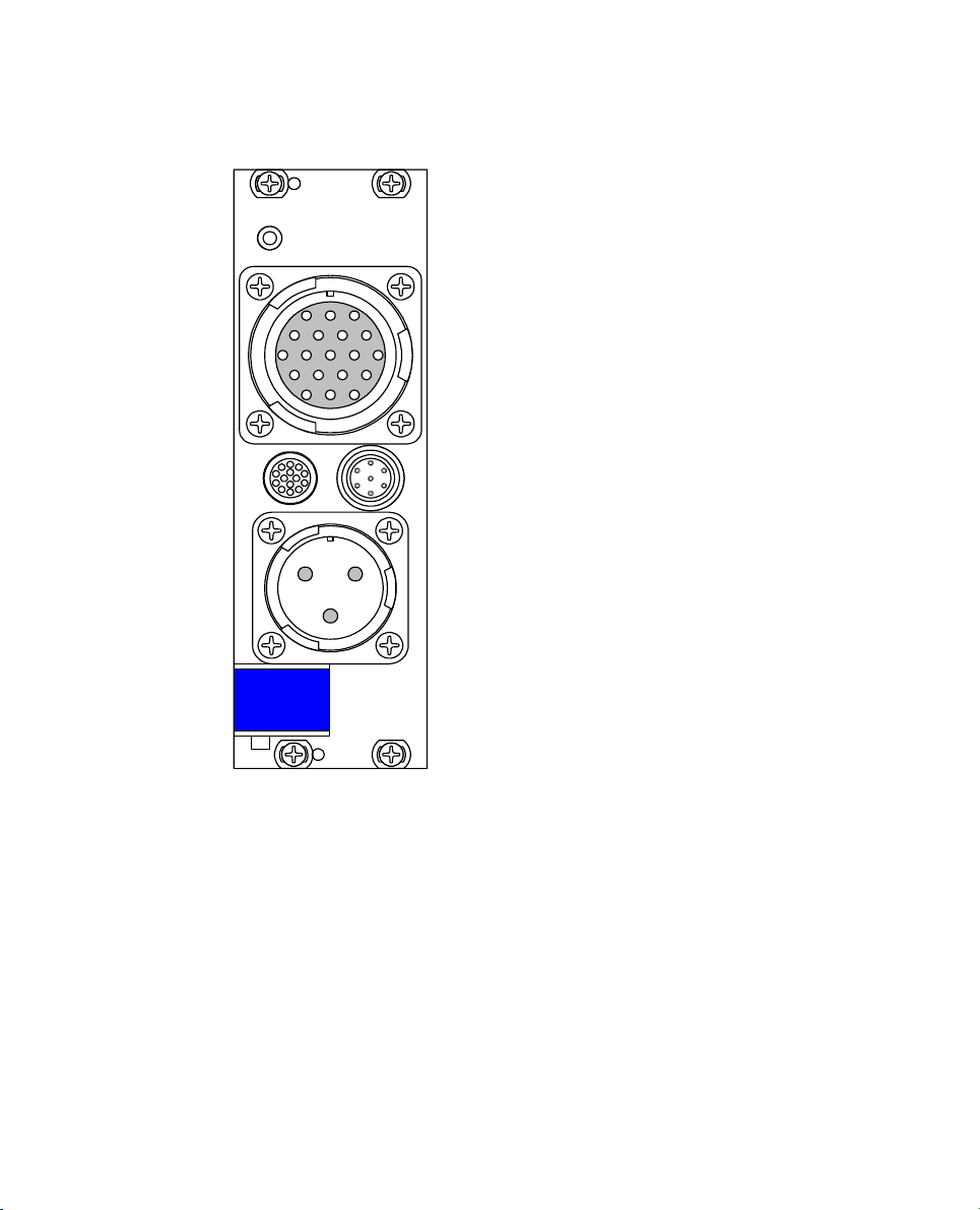
The following figure shows the front panel of the ES1392.1 High Current
Switch Board.
BATTERY
NODES
<
CTRL
ES1392.1
SUPPLY
BATTERY
INPUT
Fig. 1-2 Front Panel of the ES1392.1 High Current Switch Board
Introduction8
Page 9
1.3 Block Diagram
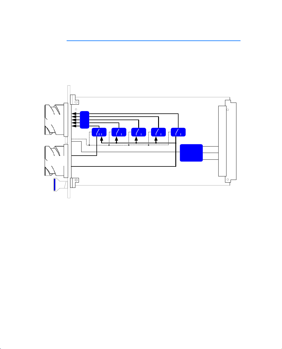
Fig. 1-3 shows the block diagram of the ES1392.1 High Current Switch Board.
The battery voltages are supplied via "BATTERY INPUT". The battery nodes
connected via "BATTERY NODES" can be switched to these battery voltages
via the switches.
BATTERY
NODES
BATTERY
INPUT
CTRL
Supply
-UBatt
+UBatt
Protection
Overcurrrent
+5 V
3
Fuses
+12 V
-12 V
Fig. 1-3 Block Diagram of the ES1392.1 High Current Switch Board
Introduction 9
Page 10

Introduction10
Page 11

2 Hardware
This chapter contains the hardware descriptions of the ES1392.1 High Current
Switch Board. It consists of the following sections:
• "Functional Description" on page 11
• "Configuring Battery Node 0" on page 12
• "Controlling the Switches" on page 13
• "Overcurrent Protection with the Status Output" on page 13
• "EEPROM" on page 13
• "Battery Voltage at the "CTRL" Connector" on page 14
• "MRC Signal" on page 14
• "Reverse-Connect Protection of the Battery Node Switches" on page 14
• "Parallel Switching of Several Battery Nodes" on page 15
• "Potential Difference between Ground and -UBatt" on page 15
• "Battery Voltage at the "BATTERY NODES" Connector" on page 15
• "Protective Measures" on page 15
2.1 Functional Description
The ES1392.1 High Current Switch Board has two groups of switch channels
which differ in terms of their maximum current rating. Battery node 0 can be
switched to either +UBatt or -UBatt whereas the other battery nodes can only
be switched to +UBatt (see Tab. 2-1).
Switch to
Battery Node
0YesYes20A
1 Yes No 20 A
2 Yes No 12 A
3 Yes No 12 A
4 Yes No 12 A
+UBatt -UBatt
Tab . 2 - 1 Switching Possibilities and Permissible Currents
Permissible
Current
Hardware 11
Page 12
2.2 Configuring Battery Node 0
Battery node 0 can be configured to be switched to either +UBatt or -UBatt.
Once the configuration has been changed, both switches remain open until,
after a delay, the new configuration becomes active. This makes it impossible
to use battery node 0 as a half bridge for fast signals.
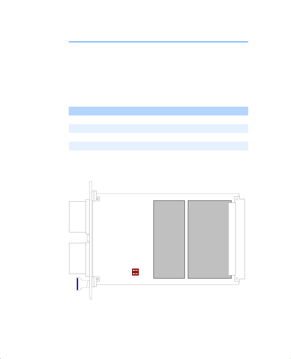
Battery node 0 can be configured using jumpers or via the "configuration
switch 0" control signal of the "CTRL" connector (see Tab. 3-3 on page 22).
Please consult Tab. 2-2 for more details on the jumper configuration or the
control signal for the relevant configuration
JP1 JP2 Control Signal Configuration
1 0 Any +UBatt
0 1 Any -UBatt
1 1 L/open +UBatt
1 1 H -UBatt
Tab . 2 - 2 Jumper Configuration and Control Signals for Configuring Bat-
tery Node 0
The position of the jumpers on the board is shown in Fig. 2-1.
JP1
JP2
Fig. 2-1 Position of Jumpers JP1 and JP2
Hardware12
Page 13

2.3 Controlling the Switches
The switches are controlled using the "control signal switch n" control signals
(see Section 3.3 on page 21).
Control Signal Switch
L/open Open
H Closed
Tab . 2 - 3 Control Signal and Switch Position
2.4 Overcurrent Protection with the Status Output
If an overcurrent is detected on one of the battery nodes, the relevant switch
is opened. After a delay of max. 800 ms, the switch is automatically closed
again to check whether the error has been recovered. If the overcurrent can
still be detected, the switch is opened again immediately. This is repeated until
there is no longer an overcurrent.
note
The cyclical current impulses which occur with an overcurrent may overstrain the
current limitation of some power supplies. In this case, the battery voltage should
be buffered with a large capacitor at the output of the power supply or a lowimpedance power resistor should be added to the battery voltage line to limit the
current.
The user is made aware of one of the switches being switched off because of
an overcurrent by the "signal switch error" status signal at the "CTRL" connector (see Fig. 3-3 on page 21).
Overcurrent Status Signal
Normal operation L
Error H
Tab . 2 - 4 Status Signal for Overcurrent Errors
For more details on protective measures, please refer to Section 2.12
on page 15.
2.5 EEPROM
The type of board (ES1392.1) and the version is stored in an EEPROM and can
be read out via a 1-Wire
Power Supply Controller Board.
®
interface on the "CTRL" connector by the ES1391.1
Hardware 13
Page 14
2.6 Battery Voltage at the "CTRL" Connector
-UBatt and +UBatt are available at the "CTRL" connector. Both voltages are
protected (see Section 2.12.2 on page 17).
2.7 MRC Signal
To keep the wiring harnesses as simple as possible, the main relay control signal (MRC signal) is routed from the "BATTERY NODES" connector to the
"CTRL" connector. The signal is protected (see section 2.12.3 on page 17).
It is not used for any other purpose on the ES1392.1 High Current Switch
Board.
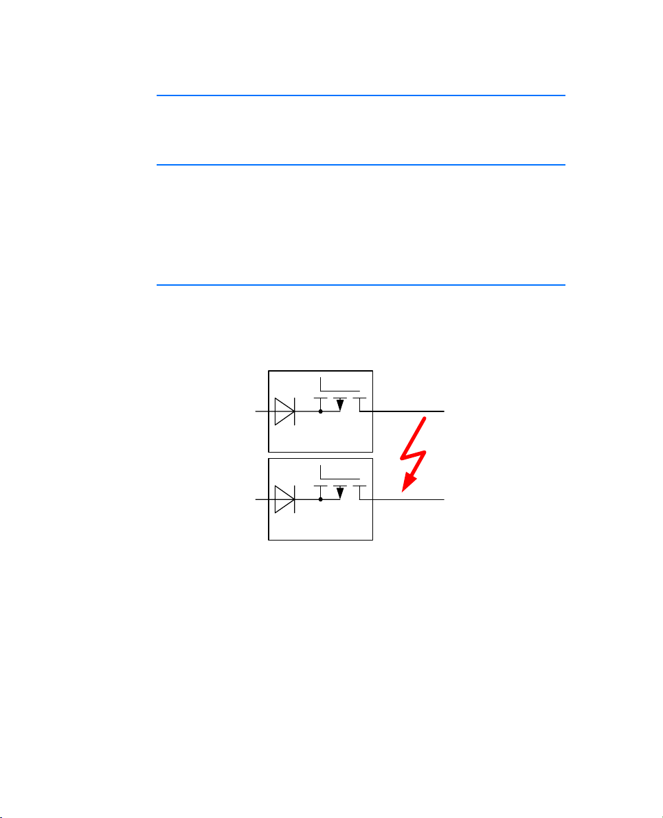
2.8 Reverse-Connect Protection of the Battery Node Switches
The switches to +UBatt are protected against voltages at the battery node
which are above the battery voltage.
This may occur, for example, in a system with two battery voltages (12 V/42 V)
if a short occurs between battery nodes of the two different battery voltages.
+UBatt_A = +12 V
ES1392
+UBatt_B = +42 V
ES1392
Battery Node
Battery Node
Fig. 2-2 Reverse-Connect Protection
Without this protection, the MOS-FET switches would still conduct current
with this kind of error without being able to be switched off. This could result
in the lower battery voltage being increased and connected consumers being
destroyed; alternatively the switch itself could be destroyed because of an
overcurrent.
The protective circuit acts as a diode (as shown in Fig. 2-2 on page 14) without
actually causing the voltage drop of a diode. The low resistance values of the
switches (including reverse-connect protection) listed in the chapter "Technical
Data" on page 29 illustrate this.
Hardware14
Page 15

2.9 Parallel Switching of Several Battery Nodes
To increase the maximum current of the battery nodes, the two 20-A battery
nodes, BN0 and BN1, can be switched in parallel. The overcurrent protection
of the switches to +UBatt of these two battery nodes is synchronized, i.e. they
are both switched off (simultaneously) when an overcurrent is detected and
then are both switched on again simultaneously.
To increase the maximum current of the battery nodes, two or all of the 12-A
battery nodes, BN2, BN3 and BN4, can be switched in parallel. The overcurrent
protection of the switches to +UBatt of these three battery nodes is synchronized, i.e. they are all switched off (simultaneously) when an overcurrent is
detected and then are all switched on again simultaneously.
note
Only the same type of battery node can be switched in parallel. 20-A and 12-A
channels cannot be combined.
The maximum overall current of 40 A must not be exceeded.
2.10 Potential Difference between Ground and -UBatt
The potential difference between ground and -UBatt must not exceed ±2 V.
Otherwise the functionality of the board can no longer be guaranteed and the
board may even be damaged.
2.11 Battery Voltage at the "BATTERY NODES" Connector
-UBatt and +UBatt are available at the "BATTERY NODES" connector. Both
voltages are protected.
2.12 Protective Measures
The battery voltages +UBatt and -UBatt supplied by the power supply to "BATTERY INPUT" are protected by fuses in their individual current paths.
The battery node switches themselves are protected electronically against overcurrent. The battery voltages, supply voltages and the MRC signal at the frontfacing connectors are protected by fuses.
There is no fuse protection of the overall current of +UBatt. The overall current
of +UBatt must not exceed 40 A.
Hardware 15
Page 16
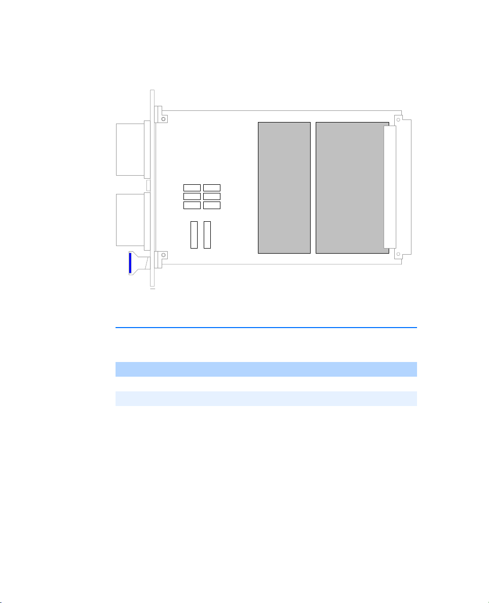
The position of the fuses on the board is shown in Fig. 2-3 on page 16 - their
specifications can be found in the following sections.
FU 222
FU 270
FU 221
FU 271
FU 220
FU 272
FU 201
FU 202
Fig. 2-3 Position of the Fuses (Component Side)
2.12.1 +UBatt and -UBatt at "BATTERY NODES"
The battery voltages output at the front-facing "BATTERY NODES" connector
are protected as follows:
Fuse Specification Ty pe Manufacturer/Order No.
FU201 20 A 80V Blade Fuse Link Pudenz / 166.7000.520
FU202 20 A 80V Blade Fuse Link Pudenz / 166.7000.520
Tab . 2 - 5 Fuse Protection of Battery Voltages +UBatt and -UBatt
Hardware16
Page 17

2.12.2 +UBatt and -UBatt at "CTRL"
The battery voltages output at the front-facing "CTRL" connector are protected as follows:
Fuse Specification Ty pe Manufacturer/Order No.
FU220 1 A, slow-
blowing
FU221 1A, slow-
blowing
NANO2 SMD Fuse Littelfuse 154.001T
NANO2 SMD Fuse Littelfuse 154.001T
Tab . 2 - 6 Fuse Protection of +UBatt and -UBatt at "CTRL"
2.12.3 MRC Signal between "BATTERY NODES" and "CTRL"
The MRC signal fed-through between the front-facing connectors "BATTERY
NODES" and "CTRL" is protected as follows:
Fuse Specification Ty pe Manufacturer/Order No.
FU222 1 A, slow-
blowing
NANO2 SMD Fuse Littelfuse 154.001T
Tab . 2 - 7 Fuse Protection of the MRC Signal
2.12.4 Supply Voltages at "SUPPLY"
The supply voltages routed from the backplane to the front-facing "SUPPLY"
connector are protected as follows:
Fuse Specification Ty pe Manufacturer/Order No.
FU271 2 A NANO2 SMD Fuse Littelfuse 154.002T
Tab . 2 - 8 Fuse Protection of the +5 V Supply Voltage
Fuse Specification Ty pe Manufacturer/Order No.
FU270 1.5 A NANO2 SMD Fuse Littelfuse 154.01.5T
Tab . 2 - 9
Fus
e Protection of the -12 V Supply Voltage
Hardware 17
Page 18

Fuse Specification Ty pe Manufacturer/Order No.
FU272 1.5 A NANO2 SMD Fuse Littelfuse 154.01.5T
. 2-10 Fuse Protection of the +12 V Supply Voltage
Tab
Hardware18
Page 19

3Pin Assignment
This chapter explains the pin assignment of the connectors of the ES1392.1
High Current Switch Board.
These are:
• ""BATTERY NODES" Connector" on page 19
• ""BATTERY INPUT" Connector" on page 21
• ""CTRL" Connector" on page 21
• ""SUPPLY" Connector" on page 22
3.1 "BATTERY NODES" Connector
Type: ITT Cannon CA02COM-E20A-48SB
Fig. 3-1 shows the pin assignment of the jack (view from the front).
M
A
N
B
P
C
D
R
E
F
L
U
K
V
T
H
S
G
Fig. 3-1 "BATTERY NODES" Connector
J
Pin Assignment 19
Page 20

Pin Signal
A -UBatt
B -UBatt
CMRC signal in
D +UBatt
E +UBatt
F CH4 out
G CH4 out
H CH3 out
J CH2 out
K CH1 out
L CH0 out
M CH0 out
N -UBatt
P Not assigned
R +UBatt
S CH3 out
T CH2 out
U CH1 out
V Not assigned
Tab . 3 - 1 "BATTERY NODES" Pin Assignment
The counterpart connector is an" ITT Cannon CA06COM-E20A-48PB".
Pin Assignment20
Page 21
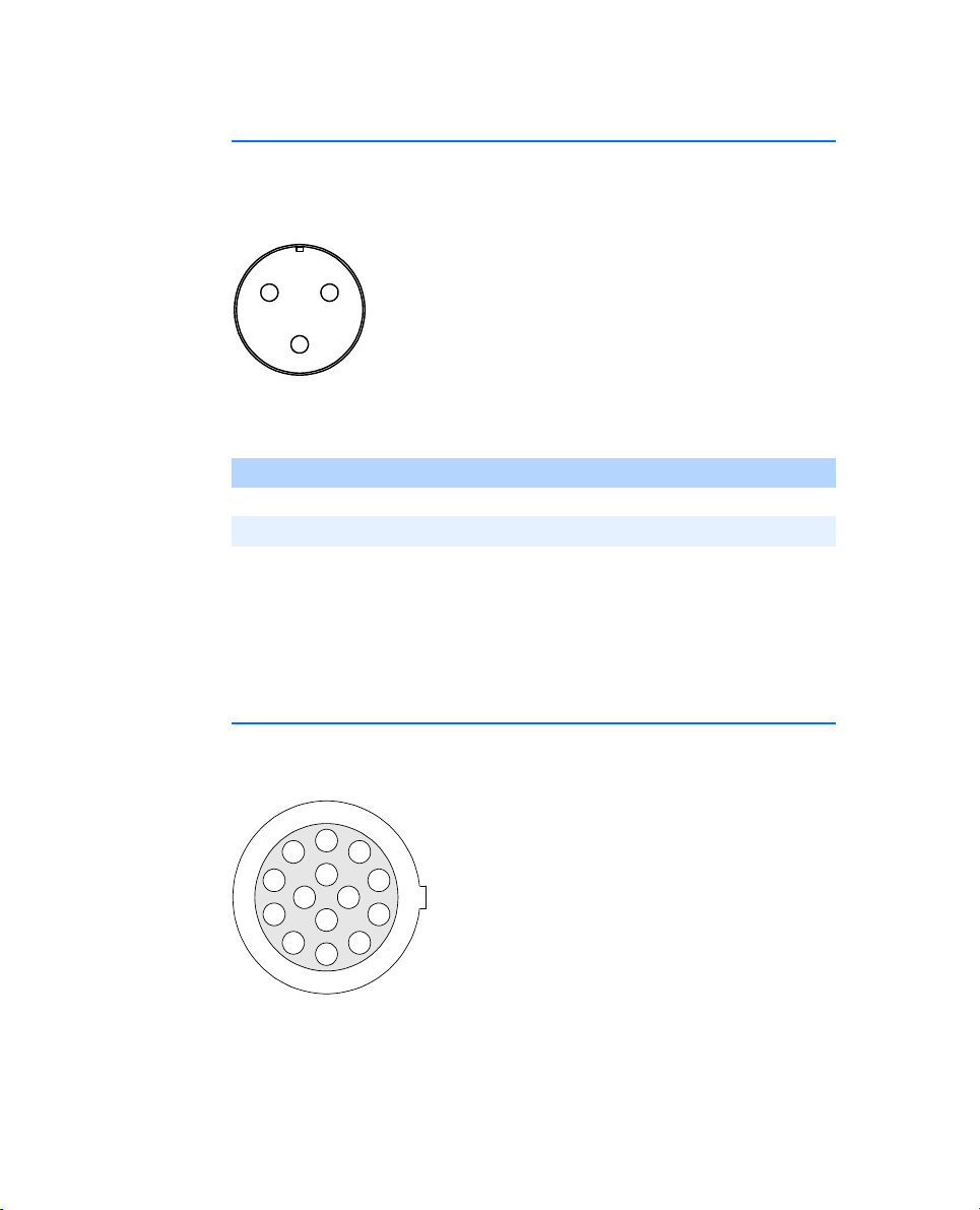
3.2 "BATTERY INPUT" Connector
Type: ITT Cannon CA02COM-E16-10PB
Fig. 3-2 shows the pin assignment of the connector (view from the front).
CA
B
Fig. 3-2 "BATTERY INPUT" Connector
Pin Signal
A +UBatt
B -UBatt
C +UBatt
Tab . 3 - 2 "BATTERY INPUT" Pin Assignment
The counterpart connector is an "ITT Cannon CA06COM-E16-10SB".
3.3 "CTRL" Connector
Type: Lemo EPG.1B.314.LLN
Fig. 3-3 shows the pin assignment of the connector (view from the front).
3
24
12
5
13 11
6
7 9
1
10
14
8
Fig. 3-3 "CTRL" Connector
Pin Assignment 21
Page 22

Pin Signal
1 Control signal switch 0 in
2 Control signal switch 1 in
3 Control signal switch 2 in
4 Control signal switch 3 in
5 Control signal switch 4 in
6 Not assigned
7 Signal switch error out
8 +UBatt out
9 -UBatt out
10 Configuration switch 0 in
11 MRC signal out
12 Switch 0-4 ground
13 ES1392.1 EEPROM signal
14 ES1392.1 EEPROM ground
Tab . 3 - 3 "CTRL" Pin Assignment
The counterpart connector is a "Lemo FGG.1B.314.CLAD76".
3.4 "SUPPLY" Connector
Type: LEMO EGG.1B.307.CLL
Fig. 3-4 shows the pin assignment of the connector (view from the front).
2
3
4 6
1
7
5
Fig. 3-4 "SUPPLY" Connector
Pin Assignment22
Page 23

Pin Signal
1-12V
2 Ground
3 Not assigned
4 +5 V
5Ground
6 +12 V
7 Not assigned
Tab . 3 - 4 "SUPPLY" Pin Assignment
The counterpart connector is a "Lemo FGG.1B.307.CLAD76".
Pin Assignment 23
Page 24

Pin Assignment24
Page 25

4Accessories
4.1 Cables
To connect the ES1392.1 High Current Switch Board to the Power Supply and
to the Controller Board two cables are required, which are described below.
4.1.1 Cable CBAV300.1-2: Connection between ES1392.1 and Power Supply (Battery Voltages)
Product Data
Short description CBAV300.1-2
Long description Cable ITT CA06COM - Ring Tongue (3fc - 2xM8)
Product part number F 00K 103 223
Specification
Length 2 m
Ty pe 2 wires, 6 mm
2
Connectors
To ES1392.1 ITT Cannon CA06COM-E16-10SB
To power supply 2 ring tongue (RT1+RT2):
DIN 46237, insulated, M8
Function ES1392.1 ITT Connector Ring Tongue Connector
+UBatt A, C brown
-UBatt B blue
Accessories 25
Page 26

4.1.2 Cable CBV300.1-0.5: Connection between ES1391 and ES1392
Product Data
Short description CBV300.1-0.5
Long description Cable Lemo 1B FGG - Lemo 1B FGG
(14mc - 14mc, 0.5m)
Product part number F 00K 103 217
Specification
Length 0.5 m
Ty pe 14 wires
Connectors
To ES1392.1 Lemo FGG.1B.314.CLAD76
(plug, solder version)
To ES1391.1 Lemo FGG.1B.314.CLAD76
(plug, solder version)
Function ES1391.1 LEMO
FGG Connector
Control signal switch 0 1 1
Control signal switch 1 2 2
Control signal switch 2 3 3
Control signal switch 3 4 4
Control signal switch 4 5 5
Not assigned 6 6
Signal switch error 7 7
+UBatt 8 8
-UBatt 9 9
Configuration switch 0 10 10
MRC signal 11 11
Accessories26
ES1392.1 LEMO
FGG Connector
Page 27

Function ES1391.1 LEMO
FGG Connector
ES1392.1 LEMO
FGG Connector
Switch 0-4 ground 12 12
ES1392.1 EEPROM signal
13 13
ES1392.1 EEPROM ground
14 14
PE Front panel Front panel
Accessories 27
Page 28

Accessories28
Page 29

5 Technical Data
This chapter contains the technical data on the ES1392.1 High Current Switch
Board.
Battery Inputs
Input voltage range 6 - 60 V
Input current Max. 40 A
High Current Switches
Overcurrent protection Yes
Automatic recovery after
overcurrent detection > 500 ms, < 800 ms (periodically)
Settling time < 50 µs
Configuration switch 0 Switch to +UBatt or -UBatt
Configuration
switch 1 - switch 4 Switch to +UBatt
Current rating
switch 0 and switch 1 20 A
Current rating
switch 1 - switch 4 12 A
Overall current Max. 40 A
Resistance of switches to +UBatt
(at 10 A) < 30 mΩ
Resistance of switches to -UBatt
(at 10 A) < 40 mΩ
Battery voltage +6 V .. +60 V
Maximum permissible potential
difference between ground and
-UBatt
Minimum voltage between
+UBatt and ground +6 V
±2 V
Te c h n i c a l D a t a 29
Page 30

High Current Switch Interface
Configuration 1 interface
Digital output channels 1
Digital output level TTL (0/5 V)
Maximum digital output current 10 mA
Digital input channels 5
Digital input level TTL (0/5 V)
Digital input current < 100 µA (I
Digital galvanic isolation No
Digital overvoltage protection Yes (60 V)
Interface for versioning data 1
Type of versioning interface 1-Wire
®
Galvanic isolation of the
versioning interface Yes
Overvoltage protection for
versioning interface No
Power Supply Interface
Configuration 1 interface
Output voltages 5 V, ±12 V
Maximum currents 2 A at 5 V
1.5A at +12V
1.5 A at -12 V
Protection Fuses
), < -1 µA (IIL)
IH
Environmental Conditions
Operating temperature 0 °C to 70 °C (32 °F to 158 °F)
Storage temperature -55 °C to +85 °C (-67 °F to 185 °F)
Relative humidity 0 to 95% (non-condensing)
Technical Data30
Page 31

Power Supply
Power consumption +5 V DC ± 5 %, 300 mA max.
±12 V DC -5% .. ±15 V +5%, 50 mA max.
Dimensions
Height 3 U
Width 8 HP (occupies 2 VME slots)
Te c h n i c a l D a t a 31
Page 32

Technical Data32
Page 33

6 ETAS Contact Addresses
ETAS HQ
ETAS GmbH
Borsigstr. 24
70469 Stuttgart Fax:
Germany
TAS Su
E
For details of your local sales office as well as your local technical support team
and product hotlines, take a look at
ETAS subsidiaries WWW: www.etas.com/en/contact.php
bsid
iaries and Technical Support
Phone:
WWW:
the ETAS website:
+49 711 3423-0
+49 711 3423-2106
www.etas.de
ETAS technical support
WWW: www.etas.com/en/hotlines.php
ETAS Contact Addresses 33
Page 34

ETAS Contact Addresses34
Page 35

Index
A
Accessories 25
Applications
5
B
Battery node 0
configuration
Battery nodes
parallel switching
Block diagram
12
9
C
Cables 25
Configuration
battery node 0
12
E
EEPROM
for version data
ETAS Contact Addresses
13
15
33
F
Features 6
Front panel
Functional description
Fuses
8
+UBatt and -UBatt
MRC signal
supply voltages
17
17
11
16
I
Introduction 5
M
MRC signal 14
O
Overcurrent protection 13
status output
13
P
Parallel switching
several battery nodes
15
Index 35
Page 36

Pin assignment 19
"BATTERY INPUT"
"BATTERY NODES"
"CTRL"
21
"SUPPLY"
Potential difference
between ground and -UBatt
Protective measures
22
21
19
15
R
Reverse-connect protection 14
S
Switch
Switching possibilities
control
13
11
T
Technical data 29
15
Index36
 Loading...