

Page 1

Reference Manual epc10x
Reference Manual
epc100
epc101
VDD33
© 2012 ESPROS Photonics Corporation
Characteristics subject to change without notice
Page 1/26 Reference Manual epc100 - V2.2
VDD
2-wire COM
2-wire COM
Interface
Interface
Parameter
Memory
V
LED
SCK
LED
LED
VDD18
GND
Processor
Voltage Regulator
CS
SPI
Controller
SI
EN
Signal
Processor
SO
f
PD
D1
Page 2

Reference Manual epc10x
Table of Contents
1. Introduction.................................................................................................................................................... 3
2. Light Curtain Principle.................................................................................................................................. 4
2.1 System Overview........................................................................................................................................................................................... 4
2.2 Light Curtain Receiver Edge..........................................................................................................................................................................6
2.3 Light Curtain Emitter Edge.............................................................................................................................................................................6
3. 2-Wire Bus...................................................................................................................................................... 7
3.1 General Description....................................................................................................................................................................................... 7
3.2 Bus Wire Considerations............................................................................................................................................................................... 8
3.3 Bus Signal Waveform.................................................................................................................................................................................... 9
4. Parameter Memory...................................................................................................................................... 10
4.1 Receiver Parameters (epc100).................................................................................................................................................................... 11
4.2 Sample Receiver Parameter Setting........................................................................................................................................................... 13
4.3 Transmitter Parameters (epc101)................................................................................................................................................................14
4.4 Sample Transmitter Parameter Setting....................................................................................................................................................... 16
5. Timing........................................................................................................................................................... 17
5.1 Overview...................................................................................................................................................................................................... 17
5.2 Timing Details.............................................................................................................................................................................................. 17
5.3 Special Cases..............................................................................................................................................................................................18
6. SPI Interface................................................................................................................................................. 19
6.1 Timing Specifications...................................................................................................................................................................................19
6.2 General Description..................................................................................................................................................................................... 19
6.3 Command List.............................................................................................................................................................................................. 20
6.4 Detailed Command Descriptions................................................................................................................................................................. 21
7. Address Programming................................................................................................................................ 24
7.1 General Description..................................................................................................................................................................................... 24
7.2 Programming Procedure..............................................................................................................................................................................25
8. Considerations for Safety Applications..................................................................................................... 26
8.1 Data Integrity on the 2-Wire Power-Bus......................................................................................................................................................26
8.2 Residual Error Rate..................................................................................................................................................................................... 26
8.3 Error Cases.................................................................................................................................................................................................. 26
8.4 Error Codes..................................................................................................................................................................................................26
© 2012 ESPROS Photonics Corporation
Characteristics subject to change without notice
Page 2/26 Reference Manual epc100 - V2.2
Page 3

Reference Manual epc10x
1. Introduction
The epc10x chip set is a general purpose CMOS integrated circuit for light-curtain applications. epc100 is used on the
receiver side (Rx) whereas epc 101 is on the emitter side (Tx). Up to 1023 devices may be connected to two respecti vely
four wires in parallel. Each device can be individually addressed by an epc100 chip which acts as the interface between a
microcontroller and the 2-wire bus. It manages the bus traffic between the microcontroller and the individual Rx and Tx
elements. Programmable fuses i.e. for the address, sensitivity, LED light pulse width, etc. allow the device to be paramet rized in the final system (OTP memory).
The microcontroller activates the Tx elements and reads the status of the Rx in a sequential manner. The status of the Rx
elements can be 'no light pulse received', 'low level light pulse received' and 'high level light pulse received'.
Each chip can be put into 'standby mode' or 'operating mode' to reduce power consumption. During 'standby mode', power
consumption is reduced and the photo diode is shorted. In the 'operation mode', the device is active and ready to receive a
light pulse generated by an LED in the emitter side of the light curtain.
During a normal scan, the microcontroller addresses one device after the other and fetches the result with a delay of three
scan periods. Thus, the microcontroller has to manage the emitter light pulses on the emitter edge of the light curtain as
well. This function is supported by the epc101 device which is the counterpart of epc100 (refer to a separate data sheet and
reference manual).
This Manual describes the various operation and programming modes in order to use Rx and interface chip epc100 and the
Tx chip epc101.
© 2012 ESPROS Photonics Corporation
Characteristics subject to change without notice
Page 3/26 Reference Manual epc100 - V2.2
Page 4

Reference Manual epc10x
2. Light Curtain Principle
2.1 System Overview
A light curtain consist of an emitter edge (Tx) and a receiver edge (Rx). The Tx edge contains a number of light emitters,
typically infrared LEDs which emit their light towards the Rx edge. The Rx edge contains typically the same number of photo
receivers like the number of emitters in the Tx edge. Typical numbers of receivers or emitters are 10, 24, 40 or every figure
between 1 and up to 1023 are possible, depending on the application. The following drawing shows a typical light curtain
setup.
© 2012 ESPROS Photonics Corporation
Characteristics subject to change without notice
Page 4/26 Reference Manual epc100 - V2.2
Micro
Controller
Out
2-Wire Bus
epc101 with LED
epc100 with PD
light cone
generated by the
LED
active light beam
light beam
number
Tx edge
➊
➋
➌
➍
➎
➏
➐
➑
➒
➓
Bus
Interface
(epc100)
Bus
Interface
(epc100)
Rx edge
Bus Termination
50Ω, 100nF
SPI-Inte
rface
Figure 1: Light curtain principle
Page 5

Reference Manual epc10x
The left side of Figure 1 shows the Tx edge containing 10 emitter elements. Each emitter element consist of an epc101 chip
with an LED and a few other components. Each of the Tx elements is connected to a 2-wire bus1, which is fed to the Rx
edge on the right side of Figure 1. The Rx edge contains 10 receiver elements, consisting of an epc100 chip with a photo
diode and a few passive components. A microcontroller which is typically but not necessarily located in the receiver edge
controls the 2-wire bus through an epc100 chip. This chip acts as a bus controller. Because every Tx and Rx element has a
unique address, the microcontroller has individual access to all bus components.
Each of the Tx elements sends light, typically infrared light, in a cone towards the Rx edge. The emitted light of one LED
illuminates usually more than one receiver element because of a rather wide cone angle2 and a small distance between the
individual elements in the edge3. If all emitters would be active at the same time, small objects between the Tx and Rx edge
would not be detected because of light bypassing. Thus, a sequential operation mode has to be established. This sequential
operation is typically like this:
1. The first Rx (Rx1) element is turned on (active mode).
2. Then, the first Tx (Tx1) element is activated so it sends a short light pulse towards the Rx edge, forming the active light
beam ➊.
3. If there is no obstacle between Tx1 and Rx1, Rx1 receives this light pulse and stores it into a local memory.
4. The microcontroller reads out the content of the memory in Rx1 and stores the value (light beam interrupted or not interrupted) into its data memory.
5. Finally, Rx1 is turned off (standby mode).
This sequence, which is also called 'scan', is repeated until all beams are checked and their status is stored in the beam
status memory of the microcontroller. The last step is to analyze the beam status memory by the microcontroller. If all
beams have the status 'not interrupted', the output of the light curtain can be set to this state. If one ore more beams are
interrupted, the output of the light curtain is set to the status 'interrupted'.
The above mentioned sequence is repeated until power is switched off. Because of the fact, that an object can enter into the
light grid right after a beam has been checked with the above mentioned procedure, up to two full scan sequences are
necessary to reliably detect an object. Thus, the overall maximum response time of the light curtain will be
tR=2∗n∗t
beamteval
(1)
where
t
R
= response time of the light curtain
n = number of elements or light beams
t
beam
= time to evaluate one beam
t
eval
= time to evaluate the beam status memory and generate the output signal
For further reference in optical design considerations please refer to the application note AN01.
1 If the LED pulse current is rather high, i.e. 1 A, two separate bus wires for the LED supply current are needed. Please refer to the data
sheet of epc101 for detailed information.
2 Typical cone angles are between 5° and 40°, depending on the application.
3 The spacing between the individual elements of a light curtain is also called 'grid spacing' and is typically in a range of a few millimeters up
to hundreds of millimeters.
© 2012 ESPROS Photonics Corporation
Characteristics subject to change without notice
Page 5/26 Reference Manual epc100 - V2.2
Page 6

Reference Manual epc10x
2.2 Light Curtain Receiver Edge
Figure 2 shows the epc100 in the light curtain application on the receiver side. It can be used in two main functions:
1. Sensor device R1 .. Rn: It senses the current pulse from the photo diode and transmits the information to the interface
device over the 2-wire bus.
2. Interface device IF: It interfaces the serial bus from the microprocessor with the 2-wire bus.
From the point of view of the microcontroller, the whole system looks like a single device with several addressable photo
diodes: the microcontroller activates one photo diode and fetches the results after a predefined time. During a normal scan,
the microcontroller addresses one device after the other and fetches the result with a delay of three scan periods.
2.3 Light Curtain Emitter Edge
On the emitter side, the epc101 controls the LEDs as the epc100 does for the photo diodes.
TP is a test point used for programming the epc101 chip with the parameters needed in the application. This test point has to
be physically accessed during final assembly of the emitter edge.
In the circuit in Figure 3, the LED current is defined by a common current source in the I
LED
line. The resistor R
LED
limits the
current through the LED and is not needed in non-safety applications. If such a resistor is inserted, a failure mode can be
detected, if more than one LED is active due to a short circuit or a failure in the epc100. It is also possible to have a common
voltage supply and to generate the LED current by a resistor.
© 2012 ESPROS Photonics Corporation
Characteristics subject to change without notice
Page 6/26 Reference Manual epc100 - V2.2
VDDVDDVDD
VDD33
I
F
epc100
GND
SO
SCK
SI
CS
µC
GND
VDD µC
VDDR
PD
VDD33
R
1
epc100
GND
VDD18
PD
VDD33
R
2
epc100
GND
VDD18
PD
VDD33
R
n
VDD
epc100
GND
VDD18
Rx Element 1 Rx Element 2 Rx Element n
Bus Termination
R
TE
100nF
R
TE
I
TE
VDD33
VDDR
epc100
GND
SO
SCK
SI
CS
µC
GND
VDD µC
VDDR
VDD
PD
epc101
GND
LED
VDD33
R
LED
+ I
LED
- I
LED
Tx Element 1
R
LED
Tx Element 2
VDD
PD
VDD33
epc101
GND
LED
R
LED
Tx Element n
VDD
PD
VDD33
epc101
GND
LED
TP
Bus Termination
R
TE
100nF
TP TP
R
TE
I
TE
Figure 2: epc100 in the light curtain application as receivers and the interface chip to the microcontroller
Figure 3: epc101 in the Tx edge application
Page 7

Reference Manual epc10x
3. 2-Wire Bus
3.1 General Description
The 2-wire bus and the power supply utilize the same two wires. The data is transmitted by modulating the current on the
power-line. The modulated current, together with the resistor in the power supply, produce a voltage signal on the line. All
devices receive this signal. The system is designed to operate with a line impedance of 50Ω (±5%). An inductor in parallel of
the resistor or a DC regulator with a lowpass feedback shape the pulses and keep the the DC voltage drop over the resistor
low. The required corner frequency of this L/R-filter is listed in the table below.
The communication interface has been designed to be used for line lengths of up to 100m and with up to 1023 sensor
devices. For line lengths of up to 3m it is possible to operate the line without termination4. Above this length the line has to
be terminated by a resistor of 50Ω (±5%) which is equal to the line impedance and a capacitor of 100nF in series.
The data rate on the 2-wire bus is set by the parameter DRATE. It also defines T
SCANmin
(refer to Chapter Timing on page 17)
and the required inductor according to Table 1. The maximum data rate allowed on the 2-wire bis is depending on the bus
length. The longer the bus wire, the lower the data rate. Table 1 shows the possible bus wire length according to the data
rate.
DRATE k Data Rate on
the 2-Wire Bus
Minimal Data Rate
Required on SPI
Interface
Corner
Frequency
L/R
Inductor
I
TE
Bus Wire
Length
5
00 8 250 kbit/s 300 kbit/s 0.5 MHz 16µH 12 … 100m
01 4 500 kbit/s 600 kbit/s 1 MHz 8µH 6 … 12m
10 2 1 Mbit/s 1.2 Mbit/s 2 MHz 4µH 3 … 6m
11 1 2 Mbit/s 2.4 Mbit/s 4 MHz 2µH ≤ 3m
Table 1: Data rate of the 2-wire communication
The default value of DRATE is 00. The parameter DRATE has to be identical for all devices on one physical 2-wire bus.
The SPI bus should be faster than the 2-wire bus, otherwise the communication does not work. Since the command length
dependent on the command type, the delay time to the next command has to be adjusted to the previous command. The
time delay can be calculated with the given data length in Table 11 on page 20.
The parameter CDET defines the optimal signal amplitude for the receiver. The maximum rate at pin VDD (5.5V) should not
be exceeded and signals which are smaller than 70% of the recommended values are not detected.
Since the command length is dependent on the command type, the delay time to the next command has to be adjusted to
the previous command. The time delay can be calculated with the given data length in Table 11 on page 20. The data
handling chain of the 2-wire communication channel is shown in Figure 4.
Figure 5 shows the different messages with the parity bits. From the interface to the sensor/transmitter device the “normal command” is used
except for the register write command. In the other direction only the register readout has a different format. Notice the different start bits
4 Dependent on the electro-mechanical design and the bus location of the edge, the termination network can be necessary. It is in the
responsibility of the system designer that the data integrity on the bus is guaranteed. Data integrity can be tested by readout bus
transmission errors. It is strongly recommended to do that during type qualification during EMI qualification tests.
5 The effective length is dependent on the electro-mechanical design of the edge. The values in the table are indicative only.
© 2012 ESPROS Photonics Corporation
Characteristics subject to change without notice
Page 7/26 Reference Manual epc100 - V2.2
Command Data
Original
Message
Parity Bits
added
Manchester
Encoder
Current
Sink
Line
Filter
A/D
Converter
Manchester
Decoder +
Error Detection
Error Correction
Received
Message
Command Data
ReceiverTransmitter
Figure 4: Data handling
Page 8

Reference Manual epc10x
which identify the direction of the transmission: 00 for the direction interface to sensor devices and 01 in the other direction. Between the
telegrams, an idle time of 2 clock periods are need to detect the start of the transmission.
3.2 Bus Wire Considerations
The electromechanical design of a system using multiple epc10x devices on a twisted pair cable with an impedance of
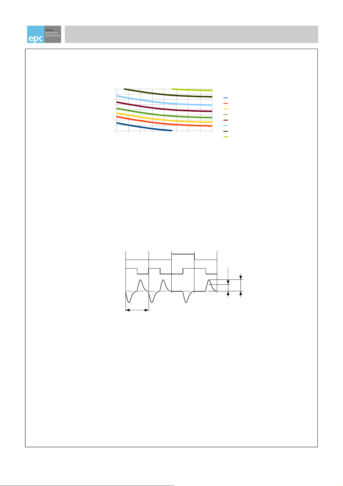
typically 100 Ohms has an impact on the overall impedance of the system. Figure 6 shows the change of the cable
impedance with smaller element pitch.
On the source side the termination is done by the resistor RTE (see Figure 2), on the other side it is highly recommended to
terminate the bus line with an AC terminator network (shown in Figure 7) which matches the overall impedance of the
system according to Figure 6. In order to avoid high DC currents in the termination resistor, a capacitor of 100nF should be
connected in series to the termination resistor. The interface device has to be placed near the L/R circuit (<1m).
© 2012 ESPROS Photonics Corporation
Characteristics subject to change without notice
Page 8/26 Reference Manual epc100 - V2.2
R
TE
100nF
1.0
1.8
3.2
5.6
10.0
17.8
31.6
56.2
100.0
0
20
40
60
80
100
120
Pitch [cm]
Impedance [Ohm]
A0A1A2A3A4A5A6A7A8A9C0C1C2P0P1P2P3P4P5P6P7P8P
9
Device Address Command Parity Bits
A0A1A2A8A
9
C0C1C2P0P1P8P9R0R1R2R3R4D0D1D14D15P0P1P8P
9
Device Address
Command
Parity Bits Parity BitsDataRegister
P0P1P8P
9
Parity Bits
D0D1D9D
10
Data
A0A1A2A8A
9
Device Address
R0R1R2R3R4D0D1D14D15P0P1P8P
9
Parity BitsDataRegister
Normal Command
Write Command
Results
Register Readout
C0C1C
2
A0A1A2A8A
9
Device Address
R0R1R2R3R
4
Register
P0P1P8P
9
Parity BitsCommand
Read Command
Figure 5: Message Structure
Figure 6: Line impedance as a function of the
element pitch on a 100 Ohm twisted pair cable
Figure 7: Bus termination network
Page 9
Reference Manual epc10x
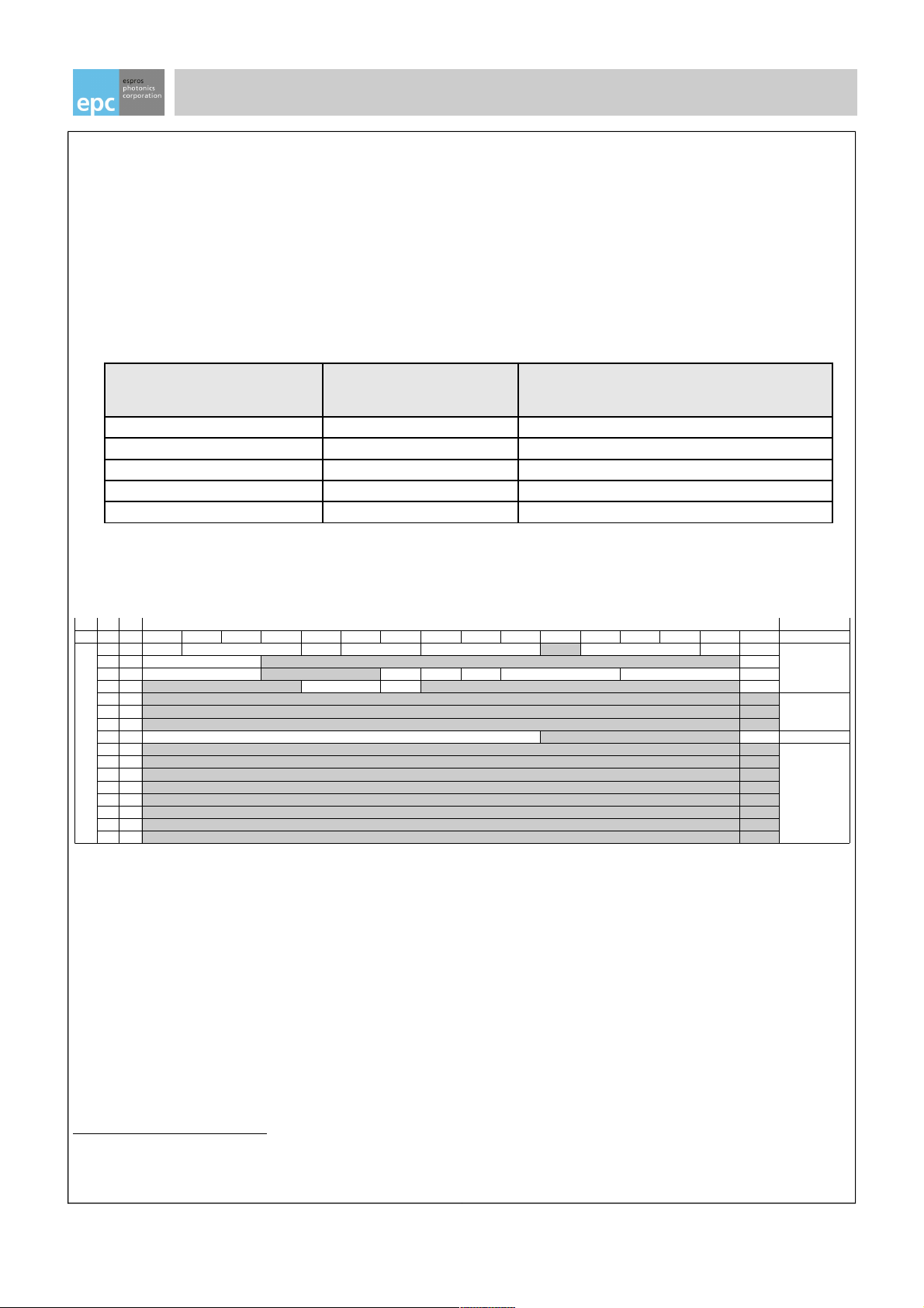
Another aspect is the distribution velocity of the electrical signals on the 2-wire bus. Since the bus wire itself as well as the
individual elements on the bus present a significant capacitance, the distribution velocity decreases with the number of
elements and the pitch between the elements.
It is important that the overall delay is less than 50% of the clock period of the transmission. E.g. if the system is operated
with 2 MBit/s data rate, the max. accepted delay must not be more than 125ns. Figure 8 shows, that a system operated at
the full speed of 2 Mbit/s, a cable length of up to 5m are possible with an element pitch down to 1cm.
Example:
If we have a system that contains 100 elements in a pitch of 10cm, the total bus length is 10m. According to Figure 8, the
delay time of a proper terminated bus is a little bit more than 100ns. Thus, such a system can be operated with the full
speed of 2MBit/s. However, we recommend to limit the bus length to the values stated in Table 1.
3.3 Bus Signal Waveform
Figure 9 pictures the Manchester encoding and the signal on the bus. The signal on the bus can be monitored with an oscilloscope and should look like in the drawing.
CDET is the threshold set in the 2-wire communication receiver of the chip to detect the communication signal on the bus.
This parameter, described in Table 6 and Table 10, can be adjusted to match the specific system requirements. Thus, the
voltage swing VS of the communication signal on the bus shall match this setting. A good principle is that the voltage swing
VS measured on the bus should be min. 25% and max. 150% above the CDET value.
Example:
If CDET is set to 200mV, the voltage swing VS should be in a range of 250 to 500 mV. Ideal for this setting is a swing
voltage VS of 400mV.
Attention:
Make sure that the voltage swing VS is in the given tolerance range at every physical location of the bus. Due to reflections
in the cable, losses of the wires (capacitive, inductive, and resistive), and the high bandwidth of the communication signals,
significant differences can occur.
© 2012 ESPROS Photonics Corporation
Characteristics subject to change without notice
Page 9/26 Reference Manual epc100 - V2.2
Message
Manchester
Signal on Bus
T
DataRate
CDET
V
S
1 1.78 3.16 5.62 10 17.7831.6256.23 100
10
32
100
316
1000
1
2
3
5
10
20
50
100
Pitch [cm]
Delay [ns]
Figure 8: Delay vs Pitch. Parameter: Line length [m]
Figure 9: Manchester encoded signal on the bus
Page 10
Reference Manual epc10x
4. Parameter Memory
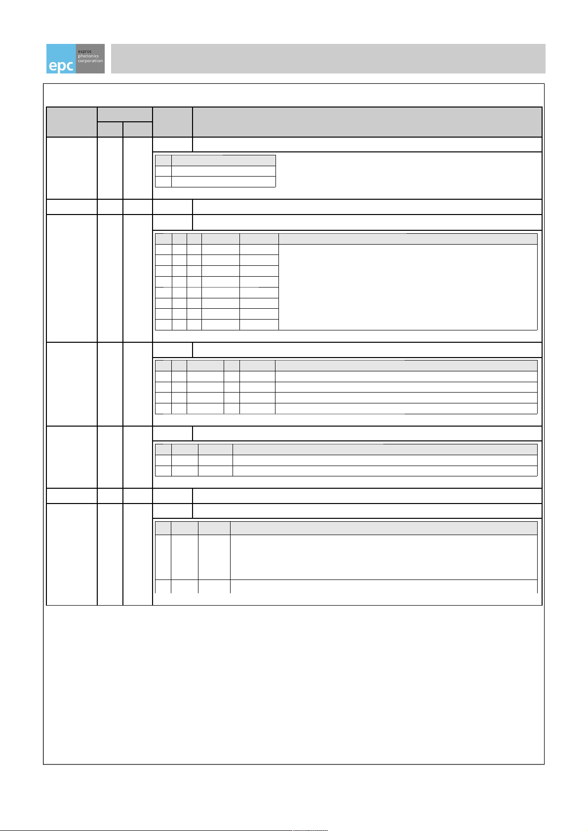
The devices epc100 and epc101 contain a memory to store the application parameters. The following classes of data are
stored on each device:
Unique chip ID and chip adjustments (factory set)
Physical device address in the application, representing the beam number
Application parameters
This data can be permanently stored in a read-only memory6 and is mirrored in a volatile memory7. At power up, the data
(except the chip ID) is copied from the ROM to the RAM. During operation, the data from the RAM is used. Both memories
are organized in 16 registers at 16 bits each. The data can be accessed on a 16-bit register base. The following table shows
the memory organization:
Non-Volatile Memory Address
Range
(Register no.)
Volatile Memory Address
Range
(Register no.)
Description
0 - 3 16 – 19 Application parameters
4 - 6 20 – 22 Trim values, factory set
7 23 Device Address
8 – 15 - Chip ID, factory set
- 24 – 31 For factory test purpose. Read only.
Table 2: Memory map overview
As shown in the table above, registers 0 – 3 and 7 are used for configuring the chip in the application. Before the devices
can be used in a given light curtain system, the required application parameters and the physical address of the chip in the
system have to be stored into the devices memories. The following table shows a parameter memory overview:
Parameters in white fields only shall be programmed. Never change the memory content of gray marked cells. Because only
complete registers can be programmed, the bits which are gray marked must be set to zero.
The RAM can only be written, if the corresponding ROM memory hasn’t been written before or if the volatile mode is active
(VMODE, refer to Table 3 on page 10 and Table 7 on page 14). The last bit of each 16-bit ROM register serves as write
inhibit bit. To write to the ROM, the microcontroller has to write to the RAM first. From there, the microcontroller can first
double check the data integrity. When a memory section is verified, the content can be transferred from the RAM memory
using the command PROG to the ROM (refer to chapter 6.4.8 Command PROG).
The device is fully operational as well without programming the ROM but data will be lost at power down. Operating the
chips in this mode is helpful during the development of the product. However, in the final application, the parameters must
be stored into the ROM memory.
6 The non-volatile memory is a one-time-programmable memory (OTP). Once the memory is programmed, the programmed values cannot
be overwritten anymore! This memory type is hereinafter called ROM.
7 Hereinafter called RAM.
© 2012 ESPROS Photonics Corporation
Characteristics subject to change without notice
Page 10/26 Reference Manual epc100 - V2.2
Bit #
ROM RAM
15 14 13 12 11 10 9 8 7 6 5 4 3 2 1 0
Register #
0 16
VMODE MODE SOFF DRATE TSTMP TPULSE POL FUSEBIT
1 17
TPER FUSEBIT
2 18
TSET SENS IVCOFF SLOW SENSH SENSN / VTHRLED FUSEBIT
3 19
CDET C2X FUSEBIT
4 20
FUSEBIT
Trimming
5 21
FUSEBIT
6 22
FUSEBIT
7 23
Address FUSEBIT
Device Address
8 24
Lot no. LSB
FUSEBIT
Chip ID
9 25
Lot no. MSB
FUSEBIT
10 26 Chip ID
FUSEBIT
11 27
Factory use only
FUSEBIT
12 28 Revision no.
FUSEBIT
13 29
no function
FUSEBIT
14 30
no function
FUSEBIT
15 31 no function
FUSEBIT
Application
parameters
Figure 10: Detailed memory map
Page 11
Reference Manual epc10x
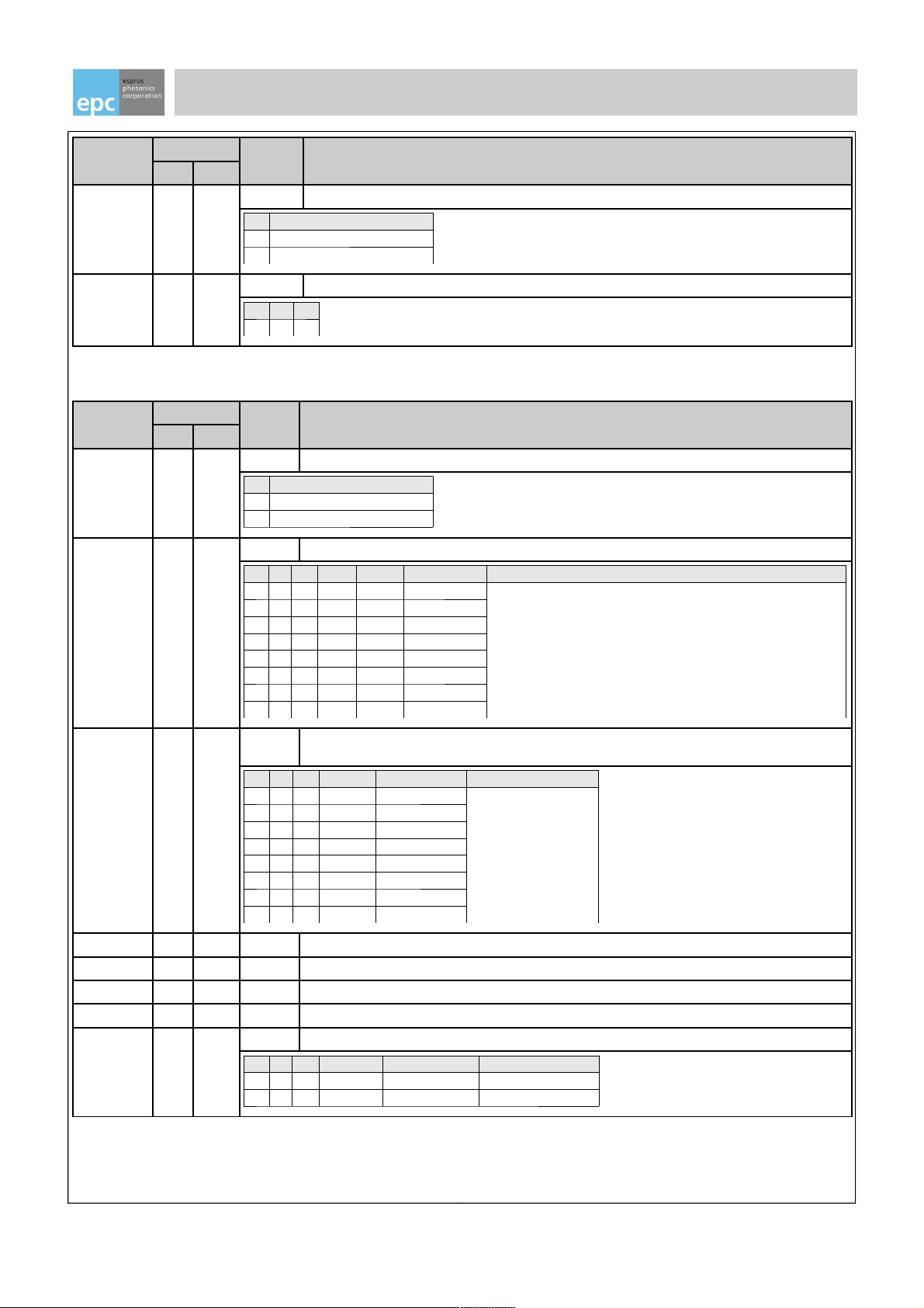
4.1 Receiver Parameters (epc100)
Parameter
Name
Register No. Bit No. Function
ROM RAM
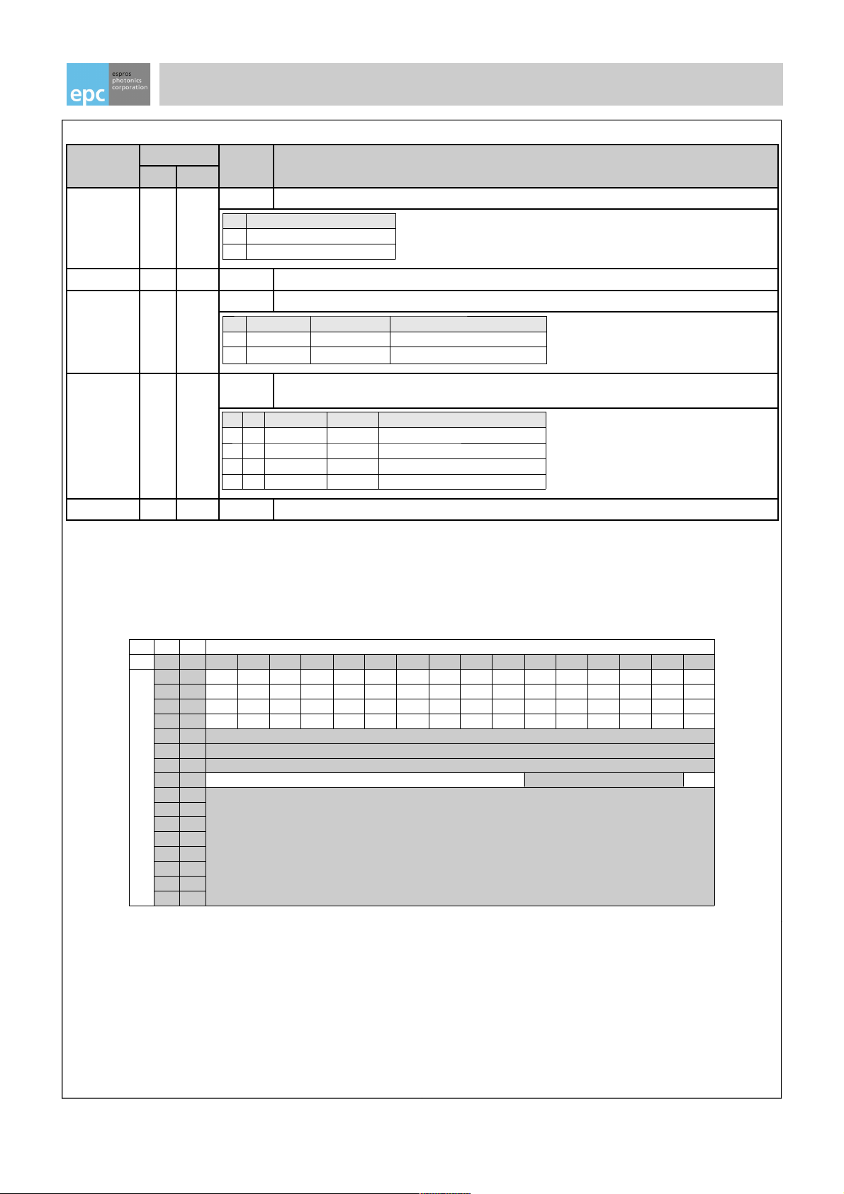
FUSEBIT 0 16 0 This bit will automatically be set when register 16 is programmed.
0 Values
0 Register 16 is not programmed
1 Register 16 is programmed
n/a 0 16 5..1 no function, must be set to “0”
TSTMP 0 16 8..6
Time stamp.
8 7 6 Values Default Recommended Setting
0 0 0 30μs X This parameter should be set to the same length as the receive window length,
given by the scanning time by the microcontroller. I.e., if the time between the
SCAN commands issued by the micro processor is 60μs, this parameter should be
set to 60μs.
0 0 1 60μs
0 1 0 90μs
0 1 1 120μs
1 0 0 150μs
1 0 1 180μs
1 1 0 210μs
1 1 1 240μs
DRATE 0 16 10..9 Data rate on the 2-wire bus
10 9 Values k Default Recommended Setting
0 0 250 kbit/s 8 X if the physical 2-wire bus length is up to 100 meters
0 1 500 kbit/s 4
1 0 1 Mbit/s 2
1 1 2 Mbit/s 1 if the physical 2-wire bus length is less than 3 meters
SOFF 0 16 11 Status of voltage regulator for internal VDD
11 Values Default Recommended Setting
0 On X when used as a receiver
1 Off when used as interface chip with 3.3V microcontroller
MODE 0 16 14..12 no function, must be set to “0”
VMODE 0 16 15 volatile mode
11 Values Default Recommended Setting
0 On X This setting allows to overwrite the RAM contents, which is useful during debugging. Once the
system is fully developed, this parameter should be set to “1”. This setting could also be useful, if
the system parameters should be changed “on the fly” in dynamic systems. it is recommended to
program the address and burn it into the ROM first. All other parameters can then be downloaded
upon power-up.
1 Off Set to “1” in the final product to avoid accidentally overwriting of the contents of the RAM registers.
Table 3: epc100 Registers 0 and 16
© 2012 ESPROS Photonics Corporation
Characteristics subject to change without notice
Page 11/26 Reference Manual epc100 - V2.2
Page 12
Reference Manual epc10x
Parameter
Name
Register No. Bit No. Function
ROM RAM
FUSEBIT 1 17 0 This bit will automatically be set when register 17 is programmed.
0 Values
0 Register 17 is not programmed
1 Register 17 is programmed
TPER 1 17 15..13 must be set to “010”
15 14 13
0 1 0
Table 4: epc100 Registers 1 and 17
Parameter
Name
Register No. Bit No. Function
ROM RAM
FUSEBIT 2 18 0 This bit will automatically be set when register 18 is programmed.
0 Values
0 Register 18 is not programmed
1 Register 18 is programmed
SENSN 2 18 3..1 Lower threshold setting of the receiver input (sensitivity).
3 2 1 Values Default Recommended Comments
0 0 0 24nA X A lower value increases the sensitivity. A too sensitive setting leads to
false readings because of shot noise of the receiver photo diode and the
internal amplifier (typ. input noise level is 7nA RMS without photo diode).
Also induced EMI can lead to false readings if the sensitivity is set too
low. The EMI sensitivity is heavily depending on the system architecture
and the electromechanical design. The better the shielding of the chip
and the photo diode and the better the PCB layout, the better the EMI
immunity. The tolerance of the threshold is approx. ±25%.
0 0 1 36nA
0 1 0 48nA
0 1 1 60nA X
1 0 0 72nA
1 0 1 84nA
1 1 0 96nA
1 1 1 108nA
SENSH 2 18 6..4 Upper threshold setting of the receiver input (light reserve level). The tolerance of the threshold is
approx. ±25%.
6 5 4 Values Default Recommended Setting
0 0 0 60nA X Set this value 50% above
the value set at SENSN,
i.e., if SENSN is set to
48nA, set SENSH to
72nA.
0 0 1 72nA
0 1 0 84nA
0 1 1 96nA
1 0 0 108nA
1 0 1 120nA
1 1 0 132nA
1 1 1 144nA
SLOW 2 18 7 no function, must be set to “1”
IVCOFF 2 18 8 no function, must be set to “0”
SENS 2 18 9 must be set to “1”
n/a 2 18 12..10 no function, must be set to “0”
TSET 2 18 15..13 Settling time delay from inactive to active mode.
15 14 13 Values Default Comments
0 0 0 0 X If T
SCAN
>=60μs
0 0 1 1 If T
SCAN
<60μs
Table 5: epc100 Registers 2 and 18
© 2012 ESPROS Photonics Corporation
Characteristics subject to change without notice
Page 12/26 Reference Manual epc100 - V2.2
Page 13
Reference Manual epc10x
Parameter
Name
Register No. Bit No. Function
RAM ROM
FUSEBIT 3 19 0 This bit will automatically be set when register 18 is programmed.
0 Values
0 Register 18 is not programmed
1 Register 18 is programmed
n/a 3 19 8..1 no function, must be set to “0”
C2X 3 19 9 Current amplitude on the 2-wire bus
9 Values Default Recommended Setting
0 8mA X X
1 16mA
CDET 3 19 11..10 Detection level for the comparator on the 2-wire bus. The level represents the optimum signal amp -
litude on the bus.
11 10 Values Default Recommended Setting
0 0 50mV X
0 1 n/a
1 0 100mV
1 1 200mV X
n/a 3 19 15..12 no function, must be set to “0”
Table 6: epc100 Registers 3 and 19
All other registers are factory set and must not be used or altered.
4.2 Sample Receiver Parameter Setting
If we are going to use a system with a maximum cable length of 3 meters, and the maximum speed on the 2-wire bus, it is
recommended to set the registers as follows:
© 2012 ESPROS Photonics Corporation
Characteristics subject to change without notice
Page 13/26 Reference Manual epc100 - V2.2
Bit #
ROM
RAM 15 14 13 12 11 10 9 8 7 6 5 4 3 2 1 0
Register #
0 16 1 0 0 0 0 1 1 0 0 0 0 0 0 0 0 X
1 17 0 1 0 0 0 0 0 0 0 0 0 0 0 0 0 X
2 18 0 0 1 0 0 0 1 0 1 0 1 1 0 1 1 X
3 19 0 1 0 0 1 1 0 0 0 0 0 0 0 0 0 X
4 20 don't use
5 21 don't use
6 22 don't use
7 23 Address don't use X
8 24
Chip ID
9 25
10 26
11 27
12 28
13 29
14 30
15 31
Figure 11: Sample parameter setting for a high speed receiver
Page 14
Reference Manual epc10x
4.3 Transmitter Parameters (epc101)
Parameter
Name
Register No. Bit No. Function
ROM RAM
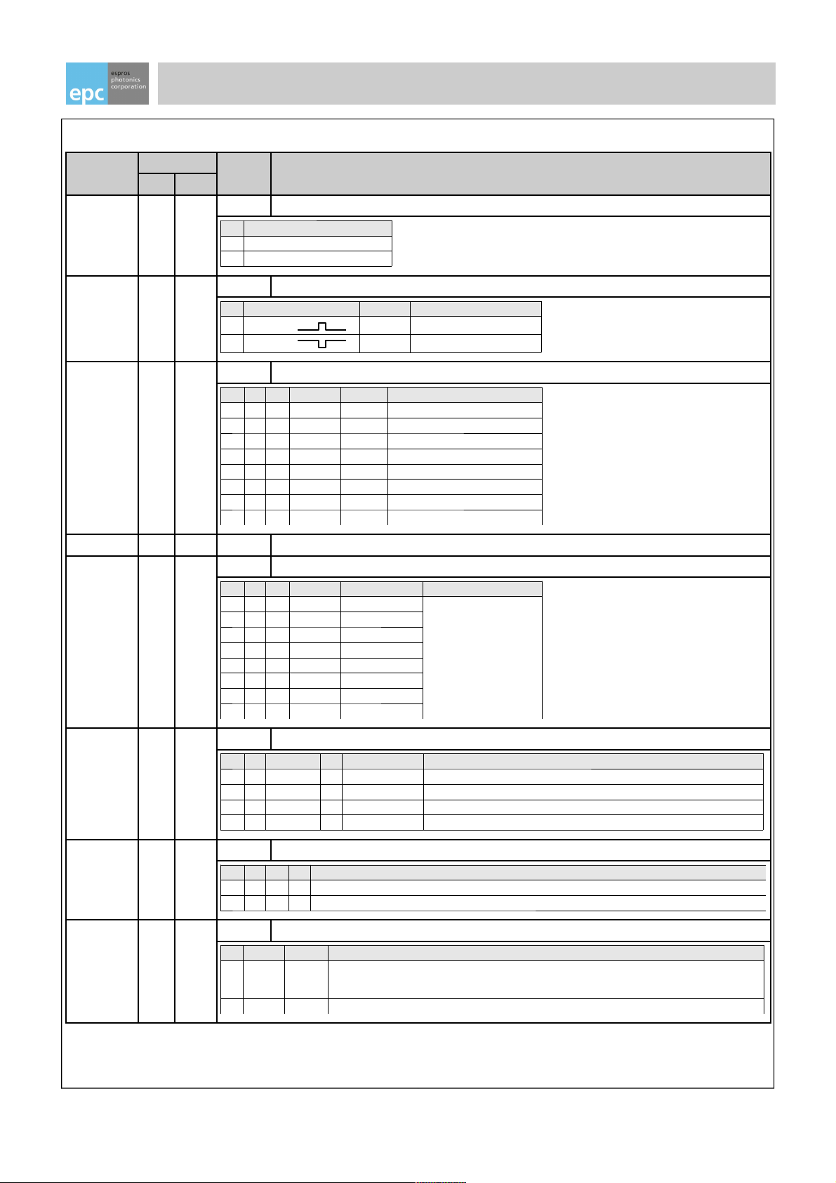
FUSEBIT 0 16 0 This bit will automatically be set when register 16 is programmed.
0 Values
0 Register 16 is not programmed
1 Register 16 is programmed
POL 0 16 1 Polarity of the LED pulse. Setting is depending on the LED driver circuitry.
1 Values Default Recommended Setting
0 active high X X
1 active low
TPULSE 0 16 4..2 Pulse length of the light pulse
4 3 2 Values Default Recommended Setting
0 0 0 1μs X
0 0 1 2μs
0 1 0 3μs
0 1 1 4μs
1 0 0 5μs X (typical setting)
1 0 1 6μs
1 1 0 7μs
1 1 1 8μs
n/a 0 16 5 no function, must be set to “0”
PDELAY 0 16 8..6 Delay after the second SCAN command to issue the light pulse.
8 7 6 Values Default Recommended Setting
0 0 0 15μs X This time shall be set so
that the light pulse is
approx. in the middle of
the receive window.
0 0 1 30μs
0 1 0 45μs
0 1 1 60μs
1 0 0 75μs
1 0 1 90μs
1 1 0 105μs
1 1 1 120μs
DRATE 0 16 10..9 Data rate on the 2-wire bus
10 9 Values k Default Recommended Setting
0 0 250 kbit/s 8 X if the physical 2-wire bus length is up to 100 meters
0 1 500 kbit/s 4
1 0 1 Mbit/s 2
1 1 2 Mbit/s 1 if the physical 2-wire bus length is less than 3 meters
MODE 0 16 14..11 Used for address allocation.
14 13 12 11 Value
1 1 1 0 Temporary value during address allocation with voltage detection (see 7. Address Programming)
0 1 0 0 Normal operation as transmitter
VMODE 0 16 15 Volatile Mode
11 Values Default Recommended Setting
0 On X This setting allows to overwrite the RAM contents, which is useful during debugging. Once the
system is fully developed, this parameter should be set to “1”. This setting could also be useful, if
the system parameters should be changed “on the fly” in dynamic systems.
1 Off Set to “1” in the final product to avoid accidentally overwriting of the contents of the RAM registers.
Table 7: epc101 Registers 0 and 16
© 2012 ESPROS Photonics Corporation
Characteristics subject to change without notice
Page 14/26 Reference Manual epc100 - V2.2
Page 15
Reference Manual epc10x
Parameter
Name
Register No. Bit No. Function
ROM RAM
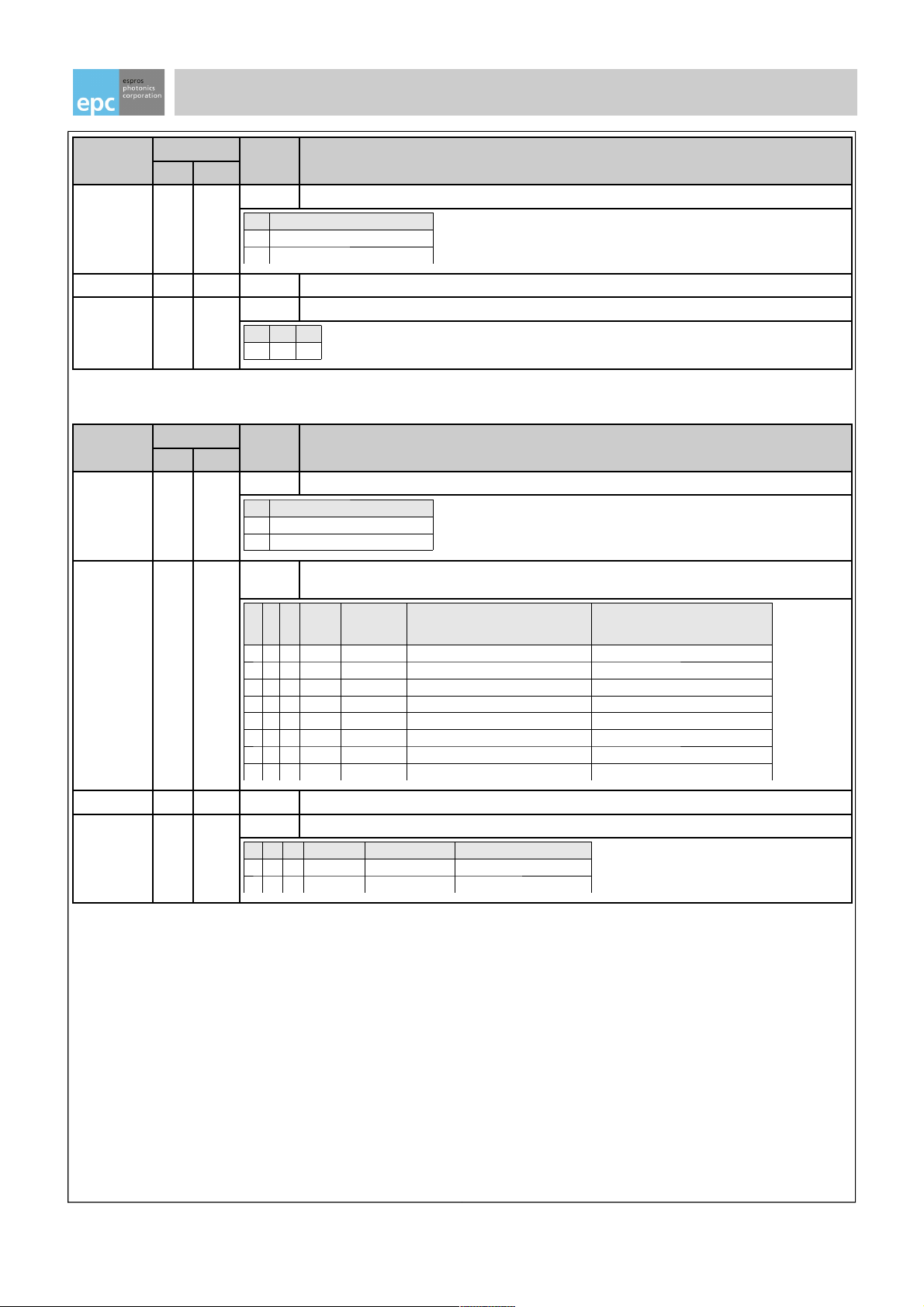
FUSEBIT 1 17 0 This bit will automatically be set when register 17 is programmed.
0 Values
0 Register 17 is not programmed
1 Register 17 is programmed
n/a 1 17 12..1 no function, must be set to “0”
TPER 1 17 15..13 must be set to “010”
15 14 13
0 1 0
Table 8: epc101 Registers 1 and 17
Parameter
Name
Register No. Bit No. Function
ROM RAM
FUSEBIT 2 18 0 This bit will automatically be set when register 18 is programmed.
0 Values
0 Register 18 is not programmed
1 Register 18 is programmed
VTHRLED 2 18 3..1 Trigger threshold to activate the address programming. Refer also to chapter 7. Address Program-
ming.
3 2 1 Values Default Recommended Setting using an
LED as photo receiver, refer to
Chapter 7. Address Programming
Using a voltage pulse on pin PD
0 0 0 0.15V X
0 0 1 0.30V X
0 1 0 0.45V
0 1 1 0.60V
1 0 0 0.75V
1 0 1 0.90V
1 1 0 1.05V
1 1 1 1.20V X
n/a 2 18 12..4 no function, must be set to “0”
TSET 2 18 15..13 Settling time delay from inactive to active mode.
15 14 13 Values Default Comments
0 0 0 0 X If T
SCAN
>=60μs
0 0 1 1 If T
SCAN
<60μs
Table 9: epc101 Registers 2 and 18
© 2012 ESPROS Photonics Corporation
Characteristics subject to change without notice
Page 15/26 Reference Manual epc100 - V2.2
Page 16
Reference Manual epc10x
Parameter
Name
Register No. Bit No. Function
ROM RAM
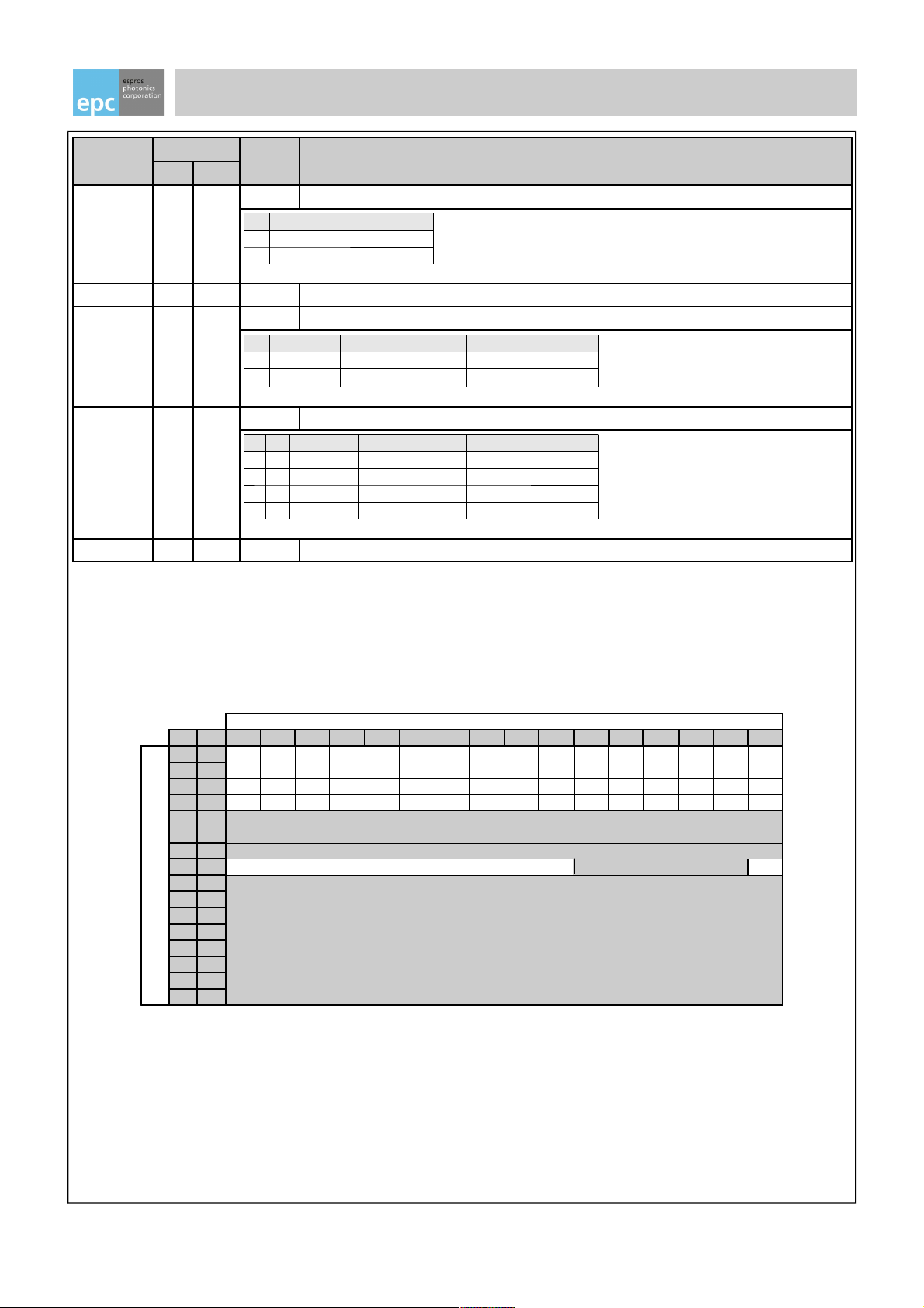
FUSEBIT 3 19 0 This bit will automatically be set when register 18 is programmed.
0 Values
0 Register 18 is not programmed
1 Register 18 is programmed
n/a 3 19 8..1 no function, must be set to “0”
C2X 3 19 9 Current amplitude on the 2-wire bus
9 Values Default Recommended Setting
0 8mA X X
1 16mA
CDET 3 19 11..10 Detection level for the comparator on the 2-wire bus
11 10 Values Default Recommended Setting
0 0 50mV X
0 1 n/a
1 0 100mV
1 1 200mV X
n/a 3 19 15..12 no function, must be set to “0”
Table 10: epc101 Registers 3 and 19
All other registers are factory set and must not be used or altered.
4.4 Sample Transmitter Parameter Setting
If we are going to use a system with a maximum cable length of 3 meters, and the maximum speed on the 2-wire bus, a
positive LED pulse with a length of 5μs, it is recommended to set the registers as follows:
© 2012 ESPROS Photonics Corporation
Characteristics subject to change without notice
Page 16/26 Reference Manual epc100 - V2.2
Bit #
ROM
RAM 15 14 13 12 11 10 9 8 7 6 5 4 3 2 1 0
Register #
0 16 1 0 1 0 0 1 1 0 0 0 0 1 0 0 0 X
1 17 0 1 0 0 0 0 0 0 0 0 0 0 0 0 0 X
2 18 0 0 1 0 0 0 0 0 0 0 0 0 0 0 1 X
3 19 0 0 0 0 1 1 0 0 0 0 0 0 0 0 0 X
4 20 don't use
5 21 don't use
6 22 don't use
7 23 Address don't use X
8 24
Chip ID
9 25
10 26
11 27
12 28
13 29
14 30
15 31
Figure 12: Sample parameter setting for a high speed transmitter
Page 17
Reference Manual epc10x
5. Timing
5.1 Overview
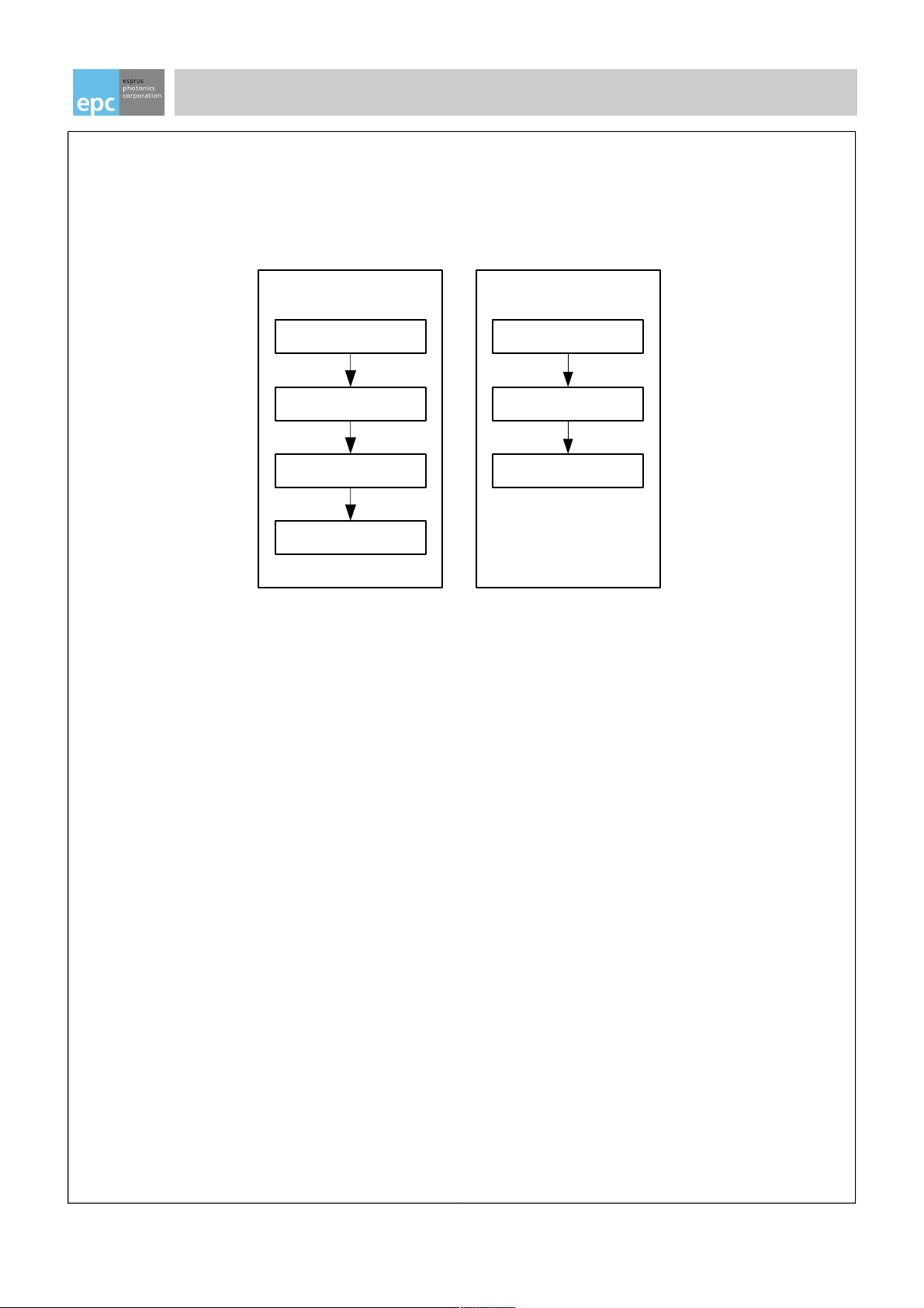
To operate the individual elements at the 2-wire bus, some steps per element are necessary. The steps differ slightly
between the Rx and the Tx elements. The following drawing shows the concept:
The individual Rx and Tx elements at the 2-wire bus are normally in a sleep mode in order to keep the overall power
consumption as low as possible. Thus, an Rx or Tx element has to be activated before it can be used. This wakeup
procedure needs a certain time until all internal operating levels have been stabilized. This time is called settling time which
can be set with the parameter TSET. Then, the receive window can be opened and the emitter can send a light pulse. After
that, the receive window must be turned off which also puts the receiver to standby. The emitter must also be put to standby.
Finally, the receive results which are stored in the Rx element can be read.
In fact, there are several steps to operate one light beam only. This needs quite a long time if everything is done in a strictly
sequential way. In order to improve the performance of the whole system, certain steps can be done in parallel. The
following chapters describe the timing processes in more detail.
5.2 Timing Details
The microprocessor controls the receivers and emitters with SCAN commands. Every SCAN command includes an address
which selects the requested receiver or emitter element.
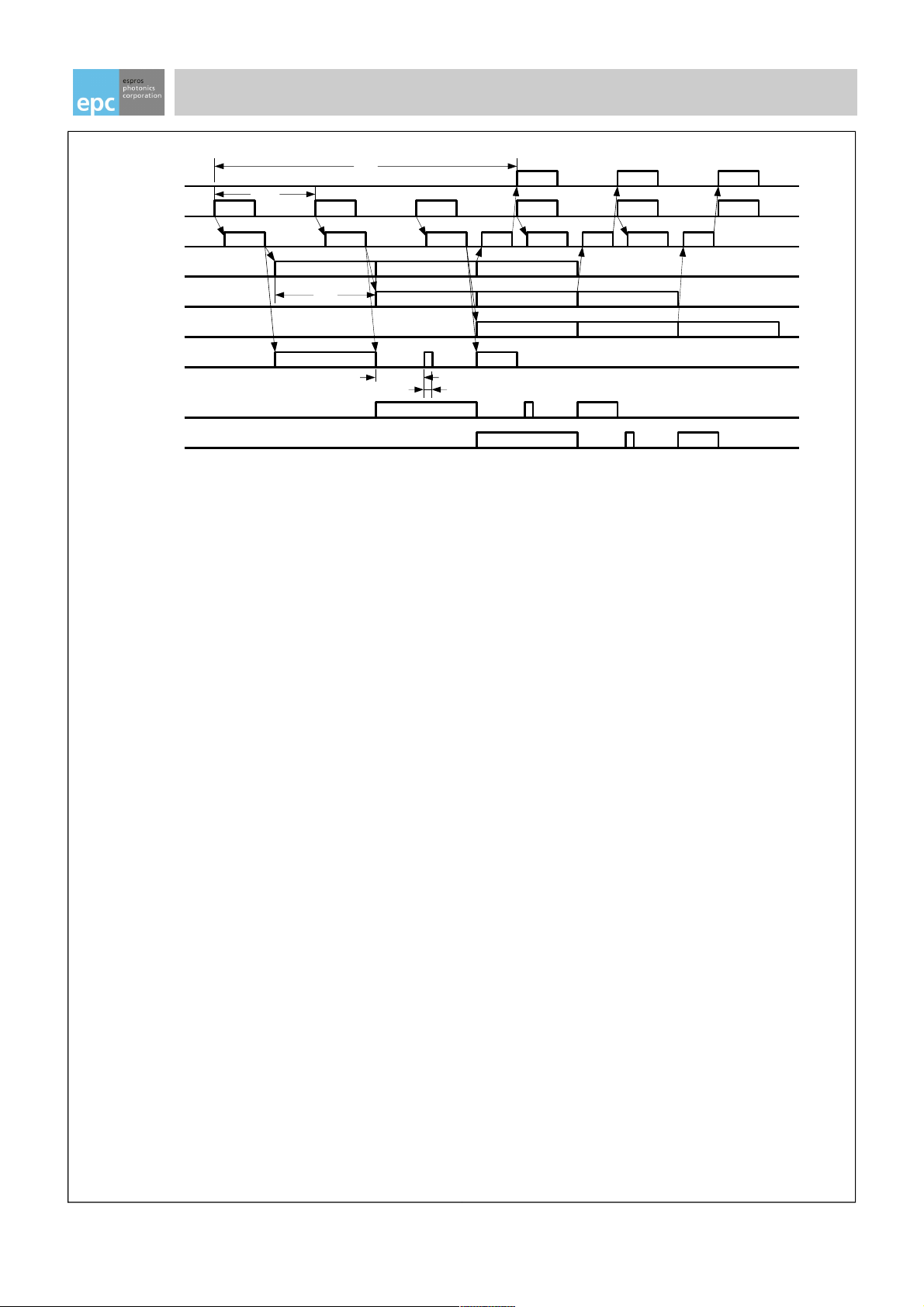
Receiver operation: A first SCAN command switches the selected Rx element from standby into the operation mode. The
process from standby to operation requires a certain time which is called settling time (see Figure 14). The settling time
minimum is 60μs. The second SCAN command opens the the reception window, where a third SCAN command closes the
reception window and puts the RX element back to standby. The fourth SCAN command fetches the received results.
Emitter operation: A first SCAN command switches the selected Tx element from standby into the operation mode. The
process from standby to operation requires a certain time which is called settling time (see Figure 14). The second SCAN
command opens the light pulse window. After the time PDELAY, one light pulse of the length TPULSE is generated. A third
SCAN command puts the emitter element back to standby. It is recommended that the light pulse is generated in the middle
of the receive window.
The whole operation is optimized for shortest possible scan periods by operating two or more Rx or Tx elements in parallel.
Figure 14 shows the timing for a settling time of one scan period (TSET=0) and the addresses given in the shortest possible
sequence.
© 2012 ESPROS Photonics Corporation
Characteristics subject to change without notice
Page 17/26 Reference Manual epc100 - V2.2
wakeup the Rx element (from
standby to operation)
wakeup the Tx element (from
standby to operation)
open the receive window
wait PDELAY and send a light
pulse
close the receive window and
put the device to standby
put the device to standby
Receiver Emitter
read the result of the last light
reception
Figure 13: Basic sequence to operate one light beam. Note that the process in the
receiver and in the transmitter are running concurrent.
Page 18
Reference Manual epc10x
where
n = element number
T
SCAN
= interval between two scan commands which is given by the micro processor
The minimum delay time between the first SCAN command and the earliest possible access of the result can be calculated
as a function of the parameter TSET and the scan period T
SCAN
:
T
DEL
=TSET 3⋅T
SCAN
The sensor device counts the number of SCAN commands on the bus to present its result at the right time. If the number of
a SCAN command is n, the result will arrive with the SCAN command n+TSET+3.
The timing of the emitter commands have to be adjusted in order to emit the light pulse near the center of the reception
window of the corresponding receiver. E.g. if the reception window length is set to 30 μs, the light pulse shall be generated
15μs after the opening of the receive window. The length of the reception window is defined by the time elapsed between
the second and the third SCAN command. The parameter TSTMP defines the time window to measure the arrival time of
the received light pulse. This result is returned in the result TIMESTAMP. The timing position of the following light pulses can
be optimized to the center of the receiving window. The resolution of TIMESTAMP is 4 bits. Thus, the value is 0000 if the
pulse is received at the beginning of the window, and 1111 if it arrived at the end. A light pulse received approx. in the middle
of the receive window would be represented as 0011, 0100 or 0101.
The minimal scan period, which is the time between two consecutive SCAN commands, is given by the communication on
the 2-wire bus: 62 bits for the command and the results have to be transmitted in this time. The minimal scan period is then
T
SCANmin
=31∗T
CLK
∗k
k is given by the parameter DRATE and varies between 1 and 8 (refer to Table 1, Table 3 and Table 7). T
CLK
is 1μs. Thus, the
minimal scan period is 31μs.
5.3 Special Cases
• If the same device is addressed again at the end of its reception window, it continues waiting for pulses. This
procedure allows to synchronize the receiver with the transmitter on an optical basis, if there is no electrical
synchronization.
• If a device detects a command during a scan operation which is not the command SCAN, it is put into standby mode.
• A SCAN command with address 0 can be used to fetch the results without starting a new scan command.
© 2012 ESPROS Photonics Corporation
Characteristics subject to change without notice
Page 18/26 Reference Manual epc100 - V2.2
SPI in
SPI out
2-Wire Bus
Rx n
Rx n+1
Rx n+2
SCAN n
SCAN n
SCAN n+1 SCAN n+2 SCAN n+3 SCAN n+4 SCAN n+5
SCAN n+1 SCAN n+2 SCAN n+3 SCAN n+4
Out n Out n+1 Out n+2
Out n Out n+1 Out n+2
T
DEL
Settling Receive Window Output, Standby
Settling Receive Window Output, Standby
Settling Receive Window Output, Standby
T
SCAN
Tx n
Tx n+1
Tx n+2
Settling Standby
Settling Standby
Settling Standby
T
PDELAY
T
PULSE
T
SET
Figure 14: Timing of the scan process
Page 19
Reference Manual epc10x
6. SPI Interface
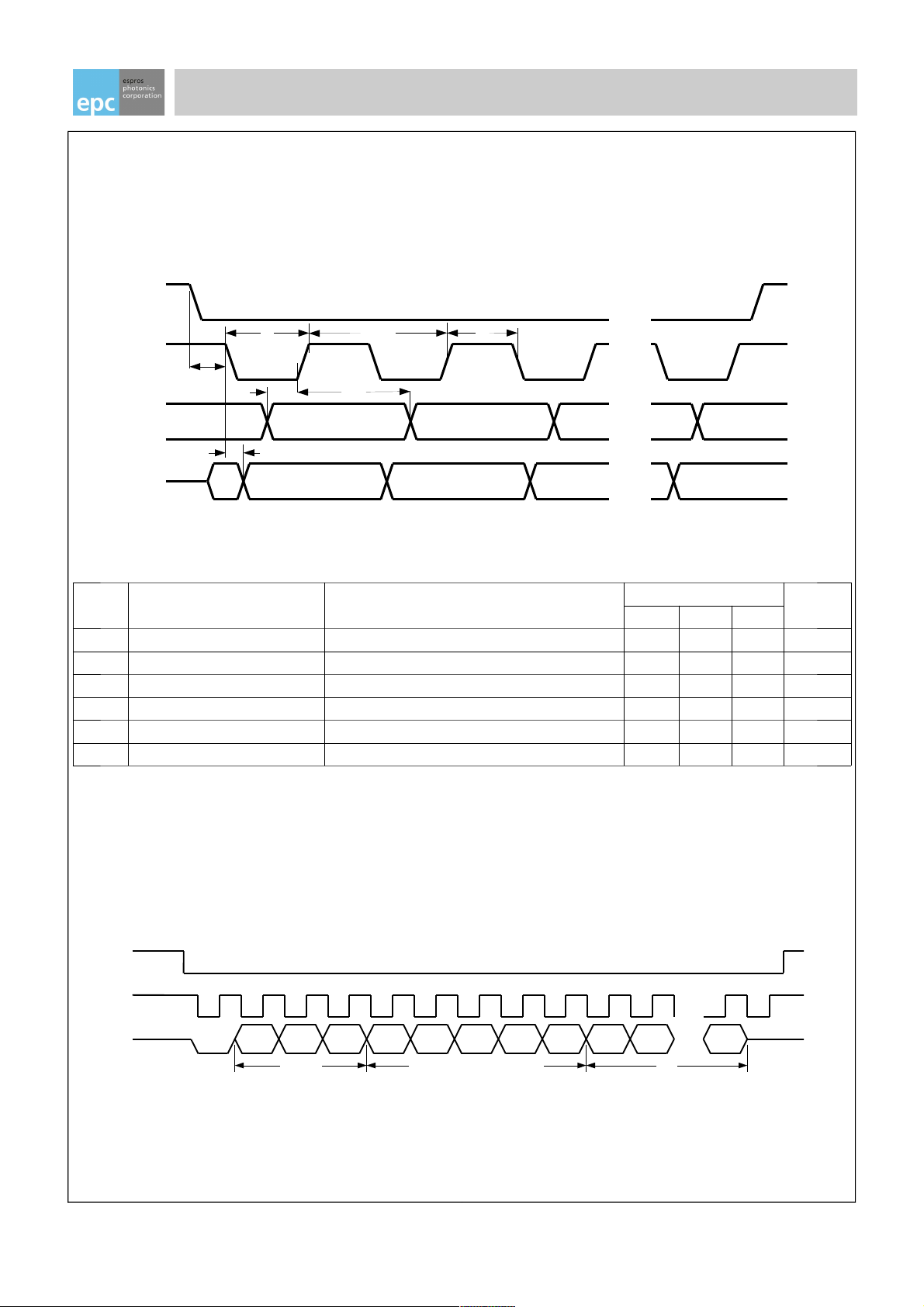
The SPI interface allows the microcontroller to communicate with the sensors over the 2-wire bus system via the interface
device.
While data are sent to the interface chip by the microcontroller, the result of the last (or more generally: a previous)
command is sent from the interface chip to the microcontroller according to the SPI protocol. The timing diagram is shown in
Figure 15).
6.1 Timing Specifications
Symbol Parameter Conditions/Comments Values Units
Min. Typ. Max.
f
SCK
SCK Clock frequency 10 MHz
tH / t
L
HIGH and LOW period of SCK 50 ns
tSU / t
Hold
Set-up and hold time SI 15 ns
t
1
Edge time CSB - SCK 50 ns
trf / t
rfSCK
Rise / fall time SO, SCK 20 ns
t
D
Data valid after SCK edge SO 20 ns
6.2 General Description
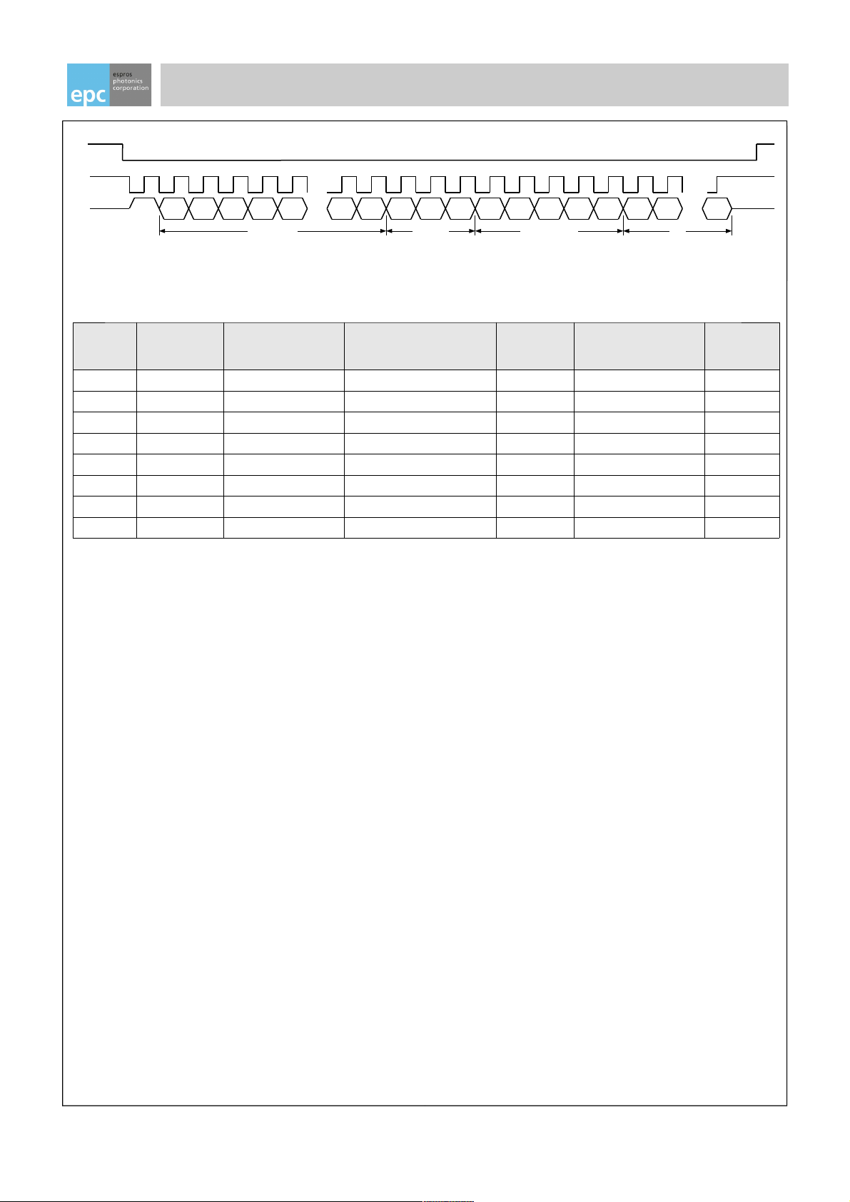
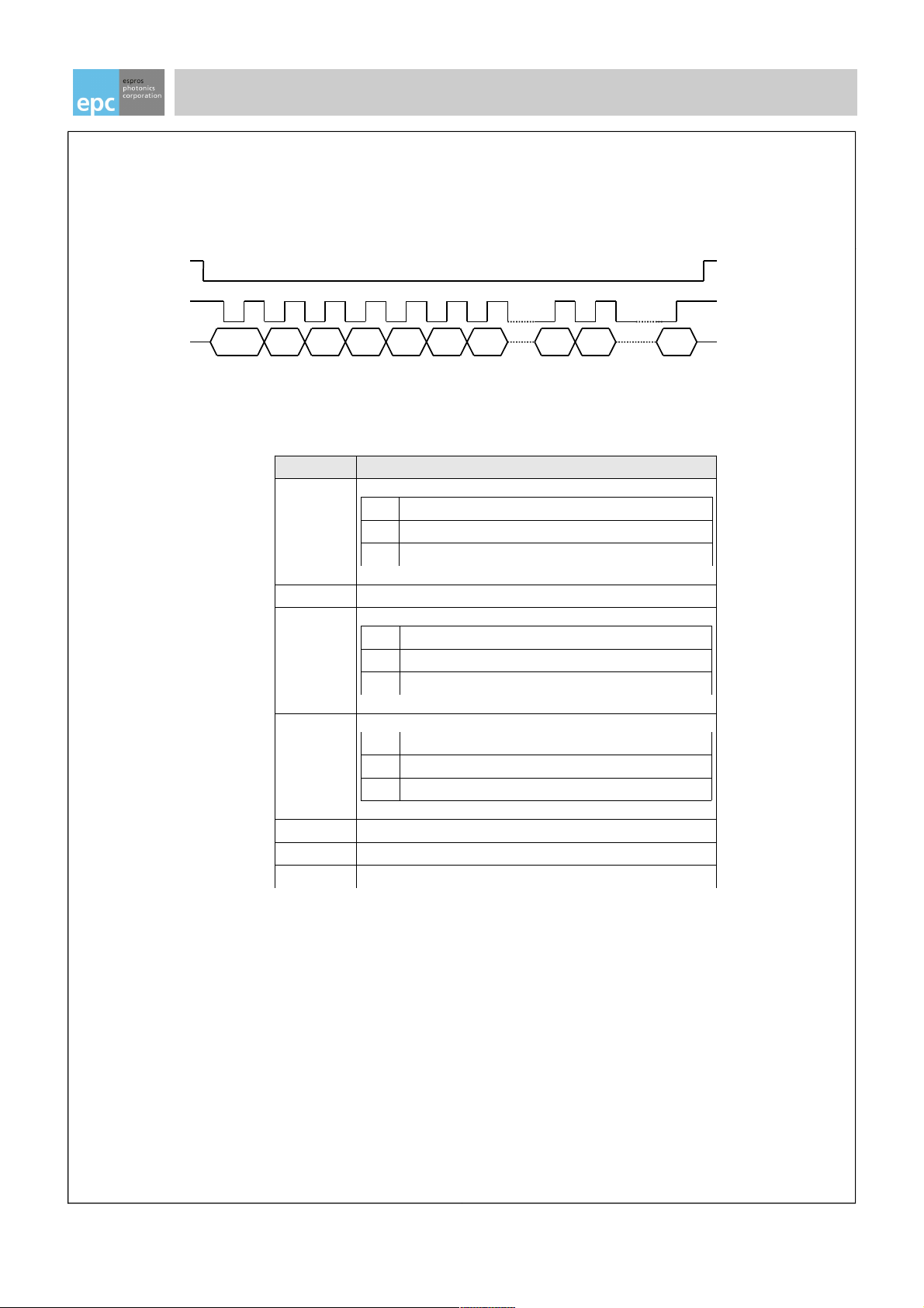
Communication is based on telegrams, which are sent and received over the 2-wire bus. Such telegrams are initiated by the
respective command to the SPI interface. The epc10x chips accept two types of commands:
1. Commands which communicate to the interface chips, also called “Direct Commands” (Figure 16).
2. Commands which communicate to the chips at the 2-wire bus, also called “Broadcast Commands” (Figure 17).
The first bit in the data stream from the microprocessor to the interface chip (SI pin) defines whether it is a command to the
interface chip (a “0”) or the the chips on the 2-wire bus (a ”1”).
© 2012 ESPROS Photonics Corporation
Characteristics subject to change without notice
Page 19/26 Reference Manual epc100 - V2.2
CS
SCK
SI
SO
t
L
t
H
t
Hold
1/f
SCK
t
1
t
SU
t
D
CS
SCK
SI C0 C1 C2 R0 R1 R2 R3 R4 D0 D1 Dn
Command
Register Address or Cmd Extension
Data
Figure 15: SPI bus timing
Figure 16: Communication to the interface device (Direct Command)
Page 20
Reference Manual epc10x
6.3 Command List
Name Command
Code
C0 .. C
2
Command
Extension Code
R0 .. R
4
Function Mode Number of data bits
on 2-wire bus
D0..D
n
Returned
Data
SCAN 000 Scan Broadcast 62 Yes
NOP 000 No operation Direct 0 Yes
READ 010 Register address Read both 97 Yes
WRITE 011 Register address Write to volatile register both 62 No
ADRA 101 Address allocation Broadcast 62 No
PROG 110 Register address Program both 62 No
TEST 111 10000 Test mode both 80 Yes
RESET 111 11001 Reset the device both 62 No
Table 11: Command list
Remarks:
• Additional SCK clock cycles have no effect.
• The telegram length on the 2-wire bus is given in the number of data clock cycles. It allows to calculate the minimum
interval between two commands.
• If an SPI command is given while another command is being transmitted on the 2-wire bus, the new command is
ignored.
• The READ and WRITE commands in the direct access mode require 2 additional SCK cycles.
© 2012 ESPROS Photonics Corporation
Characteristics subject to change without notice
Page 20/26 Reference Manual epc100 - V2.2
CS
SCK
SI
A0 A1 A2 A3 A4 R0A8 A9
D0
D1
Dn
R1 R2 R3 R4
C0
C1 C2
Device Address
Command
Register Address
or Cmd Extension
Data
Figure 17: Communication to the sensor devices (Broadcast Command)
Page 21
Reference Manual epc10x
6.4 Detailed Command Descriptions
6.4.1 Command SCAN
The command SCAN enables the addressed device, times the ongoing operation or fetches the scan result. The operation
of the command SCAN is described more in detail in Chapter 5.2 Timing Details.
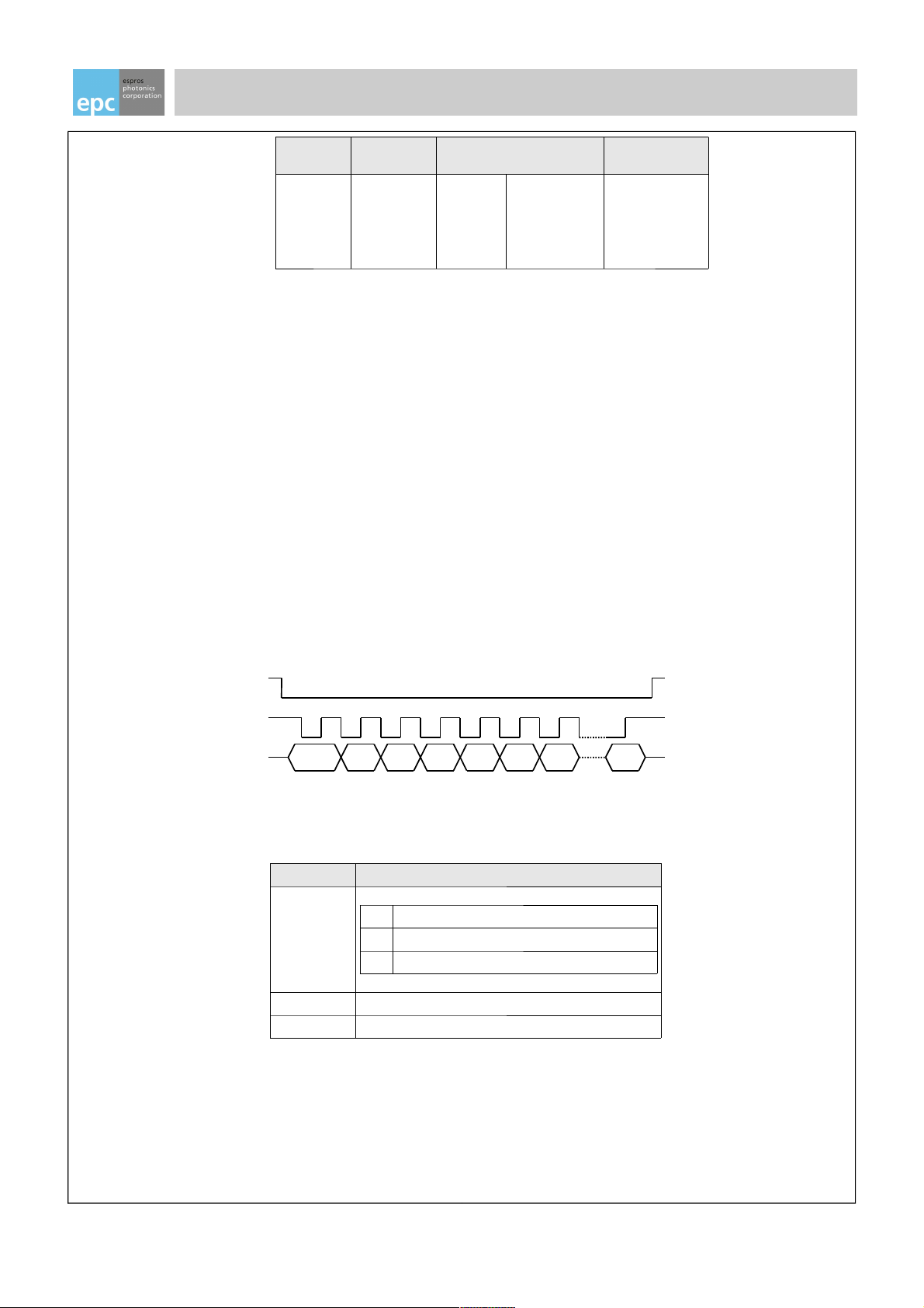
The bit N indicates whether a new result has been received. D0...D4 contains the address, D11...D20 contains the returned
data, E0...E3 contains an error code. D5...D10 are empty.
Data Bits Function
N Indicates, if new data is available
N Values
0 no new data available
1 new data available
D0 … D
3
Timestamp
D
4
Status of receiver threshold “normal”
D4Values
0 Receiver threshold set by SENSN not reached
1 Receiver threshold set by SENSN exceeded
D
5
Status of receiver threshold “high” (light reserve)
D4Values
0 Receiver threshold set by SENSH not reached
1 Receiver threshold set by SENSH exceeded
D5 … D
10
empty, not used
D
11
… D
20
Device address
E0 … E
3
Error codes, refer to Chapter 8.4 Error Codes
Table 12: Result of a SCAN command
6.4.2 Command NOP
The command NOP can be used to fetch the last received data without sending a new command. With this command it is
possible to monitor the 2-wire interface by a second interface device in a redundant system.
6.4.3 Command TEST
The command TEST issues an internal test pulse or a DC current at the PD input pin on a specific receiver. It simulates
basically a received light pulse or DC sunlight influence to check the proper functionality of the receiver(s) without using an
emitter. This mode is initialized by the command TEST and is left after a complete SCAN sequence.
© 2012 ESPROS Photonics Corporation
Characteristics subject to change without notice
Page 21/26 Reference Manual epc100 - V2.2
CS
SCK
SI
N
D
0
D
1
D
2
D
3
D
4
D
5
D
20
E
0
E
3
Figure 18: Timing of the results of a SCAN command
Page 22
Reference Manual epc10x
Code
C0 … C
2
Extension
R0 … R
4
Amplitude
D0 … D
4
Current Shape
111 10000 1xxxxx
x1xxxx
xx1xxx
xxx1xx
xxxx1x
xxxxx1
25nA
50nA
100nA
100μA
500μA DC
2mA DC
Pulse
Pulse
Pulse
Pulse
DC
DC
Table 13: Test stimulus
The applied current is the sum of different current sources: In column “Pulse Amplitude” of Table 13 a “1” means, that the
corresponding current is added. Example: 110000 generates a pulse of 75nA without DC.
6.4.4 Command RESET
The command RESET resets the device and initiates a startup. All devices can be reset simultaneously by using address 0.
6.4.5 Command ADRA
ADRA is used during the configuration of a light curtain system to allocate a logical address to the physical position of the
the emitter or receiver element.
The command ADRA stores the device address to the volatile memory only (RAM). If the device address has to be stored
permanently, the command PROG has to be used to copy the previous stored device address from the RAM register into the
ROM register. ADRA can only be used if there was no previous PROG command to the address register.
The address 0 is reserved to address all devices together or none and must not be used as an individual address.
The command ADRA generates no result.
For details refer to Chapter 7. Address Programming.
6.4.6 Command READ
The RAM and ROM can be read by the command READ. The command is extended by the register address.
The bit N indicates whether a new result has been received (broadcast mode). D0...D4 contains the address, D11...D
20
contains the returned data.
Data Bits Function
N Indicates, if new data is available
N Values
0 no new data available
1 new data available
D0 … D
4
5 bit register address
D5 … D
20
16 bit returned data (one complete register)
Table 14: Result of a READ command
6.4.7 Command WRITE
Data can be written into the RAM by using the command WRITE. The command is extended by the register address and the
data. It is only possible to write to registers if the corresponding register in the ROM has not been written yet. It is not
possible to write directly to a ROM register. If the data has to be stored into the ROM register, a subsequent command
PROG has to be used.
© 2012 ESPROS Photonics Corporation
Characteristics subject to change without notice
Page 22/26 Reference Manual epc100 - V2.2
CS
SCK
SI
N
D
0
D
1
D2D
3
D
4
D
5
D
20
Figure 19: Timing Result Data
Page 23

Reference Manual epc10x
6.4.8 Command PROG
The command PROG transfers the data from the RAM register to the corresponding ROM register. See chapter 7. Address
Programming for a detailed description.
6.4.9 Returned Results
The results at pin SO depends on one of the previous commands and can be fetched by any command or just by toggling
SCK while CS is low (=NOP).
• The data is represented with the LSB first.
• After an SPI communication the data register is cleared.
• By holding the CS line to 0 it is possible to trigger on a positive edge of SO.
• If more clock toggles SCK are issued than data can be fetched, zeros are transmitted.
© 2012 ESPROS Photonics Corporation
Characteristics subject to change without notice
Page 23/26 Reference Manual epc100 - V2.2
Page 24

Reference Manual epc10x
7. Address Programming
7.1 General Description
The device address is initially set to “00000” and the devices are not parametrized. However, all devices hold a unique chip
ID. However, due to the 2-wire bus concept, the physical location of an individual device is not known to the microcontroller.
In order to operate the light curtain, the microcontroller needs to allocate a specific receiver to a specific emitter. Usually, the
receiver at one end of the 2-wire bus gets the address 1, the next receiver the address 2 and so on. The same must be done
on the emitter side. Once all devices on the receiver and on the emitter side got their address, the microcontroller can
operate the light curtain. The address allocation, meaning the allocation of a physical location to a logical address, is usually
done in the factory of the light curtain manufacturer.
To do so, a specific address allocation procedure together with the parametrization of the devices must be executed first.
The following procedure is an example how to allocate a unique address and how to parametrize each device.
No. Step Description
1 Set the
address of
the interface
device
Set the address of the interface device with a direct command to a fix number, which should not
be 0. It is recommended to use generally the address 1023 for the interface device.
2 Parametrize
the devices
on the 2-wire
bus
The data rate DRATE of the 2-wire interface is initially set to 300 kbit/s. It shall be set to the
correct value by addressing all devices, which are initially at address 0, simultaneously. MODE
has to be set “000” or “111” depending if a current or a voltage shall be detected for the address
allocation (refer Table 7)
During this step, all other parameters in register 16 can also be set.
3 Set all other
registers
For the address allocation the following parameters should be set:
TPER = 2
SENSN = 7 (with photo diode) or 1 (with LED as a sensor, see VTHRLED, Table 9)
SLOW=1
This can be done to all devices at the same time by writing the registers to device 0.
4 Address allo-
cation
Since the devices have an open receive window, all of them are able to receive light pulses. This
mode is used to allocate the logical address to the physical location. The procedure is as follows:
1. Issue the command ADRA using address 0
2. Issue the command ADRA using address n
3. flash a light pulse to the photo diode which is connected to the chip at the physical position n
(make sure that all the other photo diodes cannot receive a light pulse). By receiving a light
pulse, the address n is stored into the RAM of the element at the physical position n. Thus, the
device, which receives a light pulse, memorizes the address n as its own address in the final
system.
This procedure has to be repeated for every individual element on the 2-wire bus. It is recommended to start with the address 1 for the element which is closest to the controller and increment the address by 1 with every individual element. In the case of a 20-beam light curtain, addresses from 1 to 20 on the receiver and on the emitter side are accessible. However, the interface chip is usually located at address 1023.
5 Address
check
It is recommended to check the correct address setting by addressing every device in the system
using the READ command. All devices addressed shall response to the READ command.
6 Address
programming
Once all addresses of all devices at the 2-wire bus are stored into the RAM (register 23), the
address should be transferred to the ROM (register 7) for each device separately by using the
command PROG. Please refer to chapter Programming Procedure.
7 Set
parameters
Parameters like TSTMP, MODE, VMODE, PDELAY, TPULSE etc. are stored into the RAM of all
devices using the command WRITE. If the global address “0” is used, all devices receive the
parameters at the same time. Since the internal voltage regulator of the interface device is not
needed, the parameter SOFF has to be set to “1” (refer to Table 3). All other devices at the 2wire bus must have a “0” for SOFF.
8 Check
parameters
The parameters should be checked by reading them back from each device using the READ
command.
© 2012 ESPROS Photonics Corporation
Characteristics subject to change without notice
Page 24/26 Reference Manual epc100 - V2.2
Page 25
Reference Manual epc10x
No. Step Description
9 Program
parameters
If all parameters are stored correctly, store the parameters into the non-volatile memory by using
the command PROG. Please refer to chapter Programming Procedure.
10 Final test To check the programming of addresses and parameters, turn off the power supply or reset all
devices and readout all addresses and parameters again.
7.2 Programming Procedure
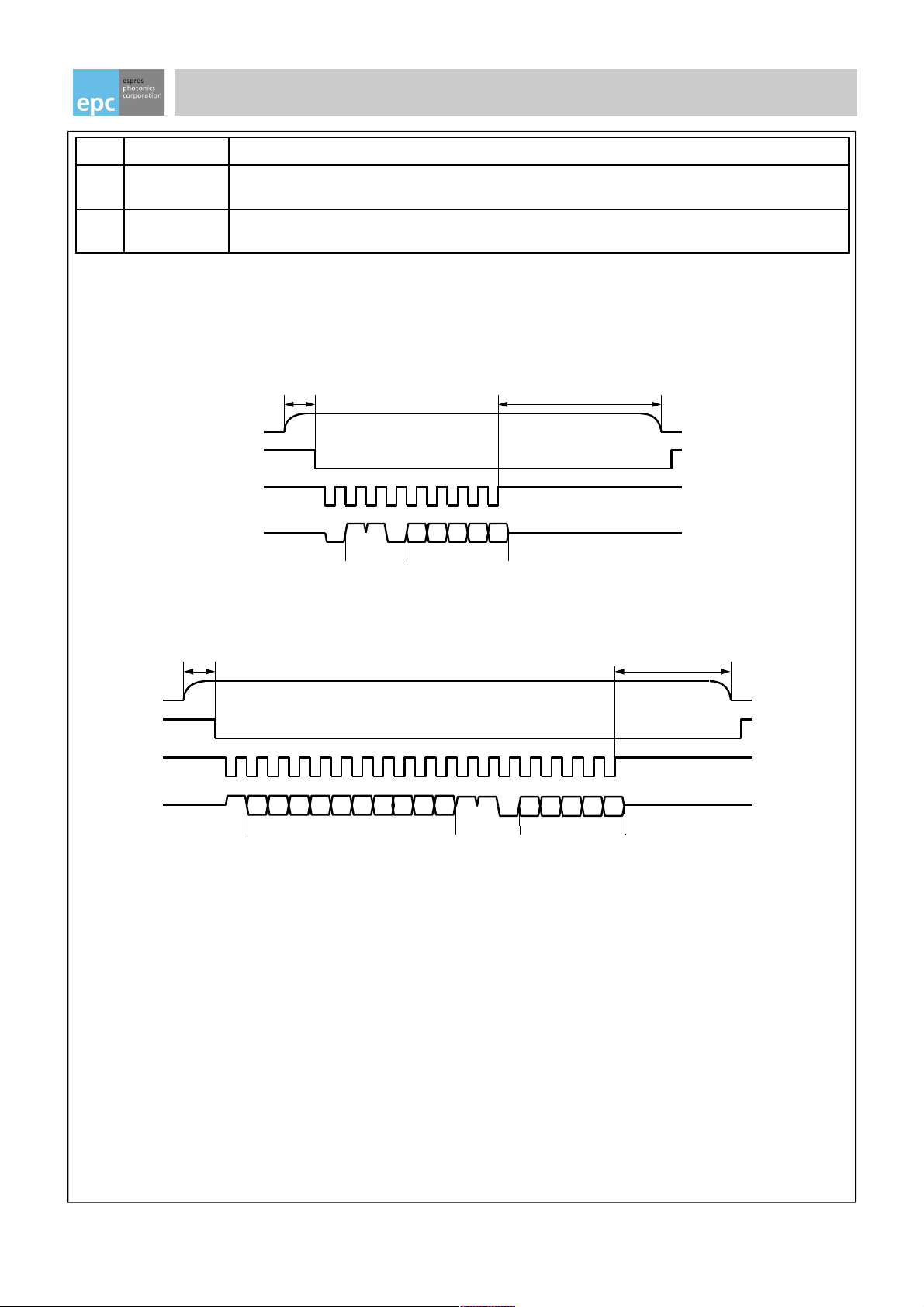
Programming the device is a transfer of the data from the RAM to the corresponding ROM register. Each 16-bit register
must be transferred individually. Thus, register 16 is transferred to register 0, register 17 to register 1, register 18 to register
2, register 19 to register 3, and register 23 to register 7. All other registers must not be used. Figure 20 shows the timing of
the programming sequence for one register:
Figure 21 shows the broadcast programming sequence for one register:
“PROG” is the PROG command sequence (110). “Register” means the address of the target register (ROM), e.g. 0, 1, 2, 3,
7. During programming, the voltage at pin VDD has to be increased to V
PROG
(7.5V) and has to be kept stable buffered during
the whole programming cycle. The timing parameters given in Figure 20 and Figure 21 have to be obeyed.
Remarks:
• It is possible to program more than one register during a VDD high cycle. Between two PROG commands a delay of
400μs is needed.
• Each register can be programmed once only (OTP).
• After programming a register, bit no. 0 of this register becomes automatically a one to indicate that the register is
programmed.
© 2012 ESPROS Photonics Corporation
Characteristics subject to change without notice
Page 25/26 Reference Manual epc100 - V2.2
R0 R1 R2R3R4
SCK
CS
VDD
SI
400μs
50μs
PROG Register
11 0
A0 A1 A2 A3 A4 A5 A6 A7 A8 A9
Device Address
5V
7.5V
50μs
VDD
CS
SCK
SI
PROG Register
R0 R1 R2R3R4
11 0
Figure 20: Direct programming procedure
400μs
7.5V
5V
Figure 21: Broadcast programming procedure
Page 26
Reference Manual epc10x
8. Considerations for Safety Applications
Since the epc10x-family chips can be used in safety related products, like machine safety light products, certain data
integrity mechanisms have been integrated. The safety concept on chip and communication level are described in this
chapter.
8.1 Data Integrity on the 2-Wire Power-Bus
Several mechanisms on different layers are implemented to guarantee a low residual error rate on the 2-wire power-bus.
Physical layer
• Modulation and medium: Current modulation on a twisted pair line is highly immune to interference.
• Start bit detection: The start pulse must have the correct orientation. Otherwise, the pulse is discarded.
• Pulse alternation: Since Manchester coding is used, the pulses need to alternate. An error is detected, if this is not
the case.
• Pulse timing: The timing of the information pulses is fixed. A missing bit (too long pause) is detected as an error.
• End bit detection: Since current modulation is used and the current is switched off when the message is completed,
the last pulse has a specified orientation.
• Sequence length: The message length is well known. A too short or too long message is detected as an error.
Data link layer
• Error control coding: If no errors have been detected on the physical layer, the received pulse sequence is processed
by an error control algorithm. Depending on the application, either 2 errors can be corrected, or 4 errors can be
detected. A higher number of errors can be detected with a reliability of 1000:1.
• Strict master-slave system: A sensor may only respond, if a request from the microcontroller was correctly received.
• Explicit addressing: Each message (master > slave and slave > master) contains the address of the sensor element.
Even if the wrong sensor replies to the microcontroller call, the error will be detected.
8.2 Residual Error Rate
Although no explicit calculations have been done yet, the residual error rate of the 2-wire power-bus is at least as good as in
the ASi. The ASi has an residual error probability of a system with Hamming distance 5 (HD5) and belongs to the DIN 19244
data integrity class I2 for an error probability p=1e-2, and to class I3 for p=1e-3.
8.3 Error Cases
Each sensor device has its unique address. The microprocessor addresses each device individually and fetches the result
some scan periods later. The result includes also the address of the answering device.
Error Cases Consequences
2 sensor answer on the same address Collision during the transmission of the result which is detected in the interface device.
Error during the scan command No device answers → no data (all zero).
Error during result transmission Error detection in the interface device.
8.4 Error Codes
Different error states are monitored:
Device Error Action Error Code
E0 … E3
1 Sensor Non-correctable error in the received telegram Device doesn't response -
2 Sensor Command to fetch the result too early Normal answer -
4 Interface No answer from the sensor device Result data zero -
5 Interface Non-correctable error in the received telegram Error reported 1xxx *)
6 Interface Return telegram not complete Error handling procedure 0100
Table 15: Error states
*) The last three error bits contain the number of detected errors.
© 2012 ESPROS Photonics Corporation
Characteristics subject to change without notice
Page 26/26 Reference Manual epc100 - V2.2
32/<7(&*PE+ 3RO\WHF3ODW] ':DOGEURQQ *(50$1<
7HO)D[ (0DLORHN#SRO\WHFGH ZZZSRO\WHFGH
 Loading...