

Ericsson PTF10162 Datasheet

PTF 10162
18 Watts, 860–960 MHz
GOLDMOS
™
Field Effect T ransistor
Description
The PTF 10162 is an 18 Watt LDMOS FET intended for large signal
amplifier applications from 860 to 960 MHz. It operates at 55% efficiency
with 15 dB of gain. Nitride surface passivation and full gold metallization
ensure excellent device lifetime and reliability.
Typical Output Power & Efficiency vs. Input Power
24
20
Output Power
16
12
8
4
Output Power (Watts)
0
0.0 0.3 0.5 0.8 1.0
Input Power (Wa tts)
VDD = 26 V
I
f = 960 MHz
= 130 mA
DQ
Efficiency
80
70
60
50
40
Efficiency (%)
30
20
• Performance at 960 MHz, 26 Volts
- Output Power = 18 Watts
- Power Gain = 15 dB Typ
- Efficiency = 55% Typ
• Full Gold Metallization
• Silicon Nitride Passivated
• Excellent Thermal Stability
• Back Side Common Source
• 100% Lot Traceability
10162
A-1234569855
Package 20222
RF Specifications (100% T ested)
Characteristic Symbol Min T yp Max Units
Common Source Power Gain
(V
Power Output at 1 dB Compression
(V
Drain Efficiency
(V
Load Mismatch Tolerance
(V
all phase angles at frequency of test)
All published data at T
= 26 V , P
DD
= 26 V , IDQ = 130 mA, f = 960 MHz) P-1dB 18 2 0 — Watts
DD
= 26 V , P
DD
= 26 V , P
DD
= 18 W, IDQ = 130 mA, f = 960 MHz) G
OUT
= 18 W, IDQ = 130 mA, f = 960 MHz) h 50 55 — %
OUT
= 18 W, IDQ = 130 mA, f = 960 MHz— Y — — 5:1 —
OUT
= 25°C unless otherwise indicated.
CASE
ps
14 15 — dB
e
1
PTF 10162
)
)
y
s
e
Electrical Characteristics (100% T ested)
Characteristic Conditions Symbol Min T yp Max Units
Drain-Source Breakdown Voltage VGS = 0 V , ID = 25 mA V
(BR)DSS
Drain-Source Leakage Current VDS = 28 V , VGS = 0 V I
Gate Threshold Voltage VDS = 10 V , ID = 75 mA V
Forward Transconductance VDS = 10 V , ID = 0.5 A g
DSS
GS(th)
fs
65 — — Volts
— — 1.0 mA
3.0 — 5.0 Volts
— 0.9 — Siemens
Maximum Ratings
Parameter Symbol Value Unit
Drain-Source Voltage V
Gate-Source Voltage V
Operating Junction T emperature T
T otal Device Dissipation P
DSS
GS
J
D
Above 25°C derate by 0.33 W/°C
Storage T emperature T
Thermal Resistance (T
= 70°C) R
CASE
STG
qJC
65 Vdc
±20 Vdc
200 °C
58 Watts
150 °C
3.0 °C/W
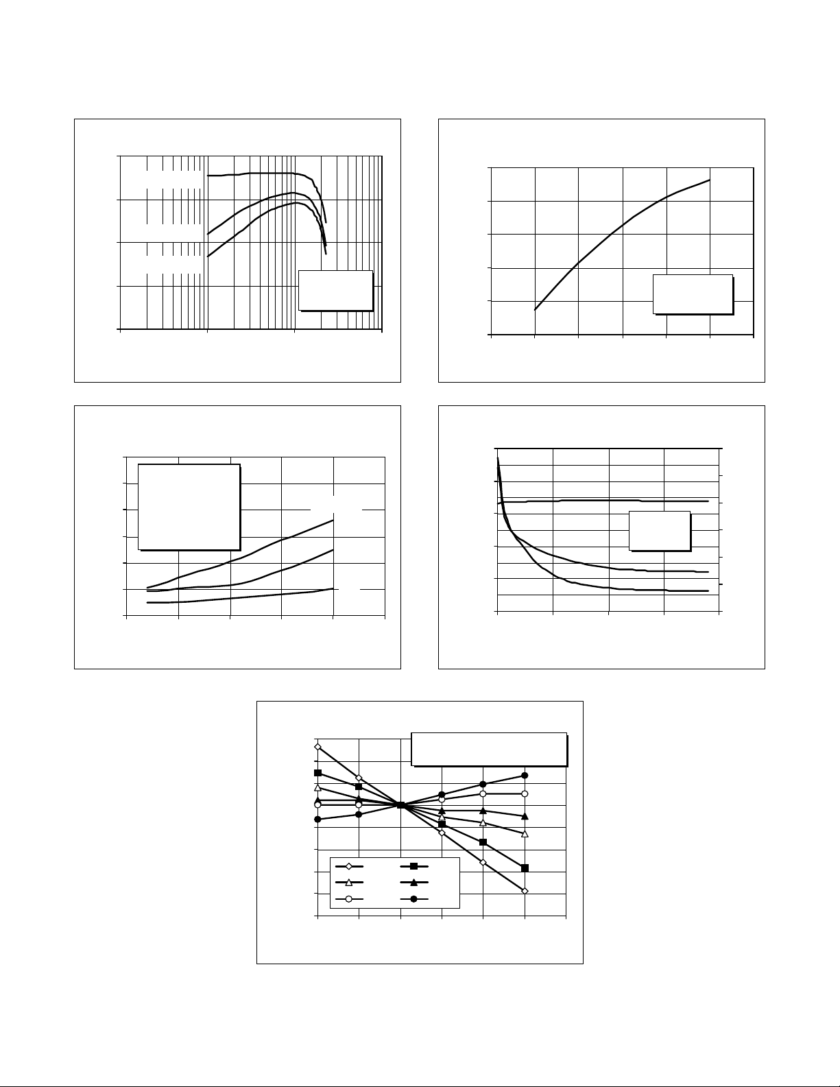
Typical Performance
Typical P
, Gain & Efficiency
OUT
vs. Frequency
21
Output P ower
20
19
18
17
Gain
16
15
Gain (dB) & Output Power (W
860 880 900 920 940 960
VDD = 26 V
= 130 mA
I
DQ
Frequency (MHz)
(at P-1dB)
Efficiency
70
65
60
55
50
45
Efficiency (%
40
35
Broadband Test Fixture Performance
20
Efficiency (%)
16
Gain (dB)
12
Gain
8
4
920 930 940 950 960
Frequency (MHz)
VDD = 26 V
= 130 mA
I
DQ
= 18 W
P
OUT
Return L oss (d B )
60
50
40
30
0
20
- 5
-10
-15
10
-20
-25
0
Efficienc
Return Los
2
e
PTF 10162
16
IDQ = 130 mA
15
IDQ = 65 mA
14
IDQ = 35 mA
13
Power Gain (dB)
12
0.1 1.0 10.0 100.0
VDD = 26 V
f = 960 MHz
Output Pow er (Watts)
Inter modulation Distort ion vs. O utput Pow er
(as measured in a broadband circuit)
0
VDD = 26 V
-10
= 130 mA
I
Power Gain vs. Output Power
-20
-30
IMD (dBc)
-40
-50
-60
DQ
= 959.900 MHz
f
1
=960.000 MHz
f
2
0 5 10 15 20 25
Output Power (Watts-PEP)
3rd Order
5th
7th
Output Power
(at 1 dB Compression)
vs. Supply Voltage
24
22
20
18
IDQ = 130 mA
16
Output Power (Watts)
14
22 24 26 28 30 32 34
f = 960 MHz
Supply Voltage (Volts)
Capacitance vs. Supply Volt age
50
40
C
gs
30
20
Cds and Cgs (pF)
10
0
0 10203040
C
ds
Supply Voltage (Volts)
VGS = 0 V
f = 1 MHz
C
rss
6
5
4
3
2
1
0
Crss (pF)
Bias Voltage vs. Temper at u r e
1.03
1.02
1.01
1.00
0.99
0.98
Bias Voltage (V)
0.97
0.96
0.95
-20 0 20 40 60 80 100
0.075 0.33
0.585 0.84
1.095 1.35
Voltage normalized to 1.0 V
Series show current (A)
Temp. (°C )
3
 Loading...