

Ericsson PTF10161 Datasheet

PTF 10161
E
165 Watts, 869–894 MHz
GOLDMOS® Field Effect T ransistor
Description
The PTF 10161 is an internally matched,165 watt GOLDMOS FET
intended for large signal amplifier applications from 869 to 894 MHz.
It typically operates with 50% efficiency and 16 db of gain. Nitride
surface passivation and full gold metallization ensure excellent device
lifetime and reliability.
Typical Output Pow er & Efficiency vs. Input Pow er
180
Efficiency
140
100
VDD = 28.0 V
= 1.5 A Total
I
60
Output Power (Watts)
20
012345678
Output Power
Input Power (Watts)
DQ
f = 880 MHz
60
45
30
fficiency (%)
15
0
• INTERNALLY MA TCHED
• Performance at 894 MHz, 28 Volts
- Output Power = 165 Watts
- Power Gain = 16.0 dB Typ
- Drain Efficiency = 50% Typ
• Full Gold Metallization
• Silicon Nitride Passivated
• Back Side Common Source
• 100% Lot Traceability
10161
1234560055
Package 20250
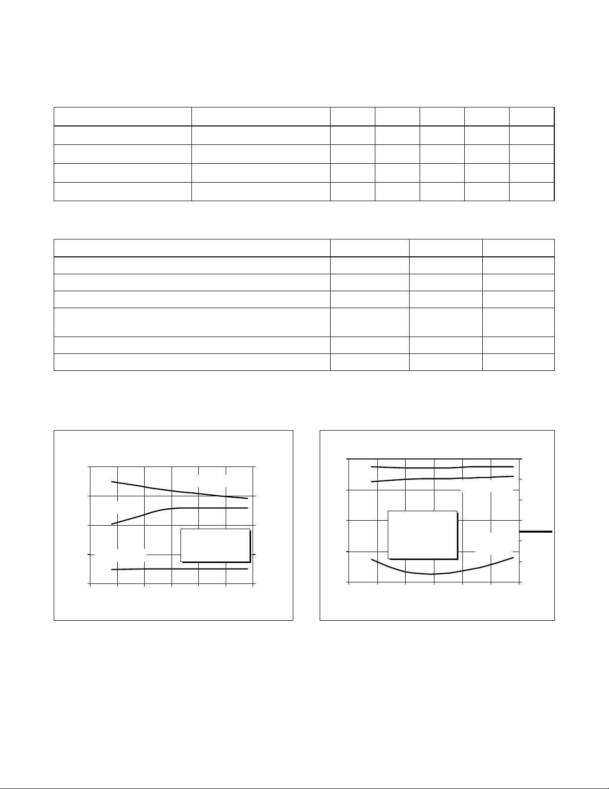
RF Specifications (100% T ested)
Characteristic Symbol Min Typ Max Units
Gain
(V
Power Output at 1 dB Compression
(V
Drain Efficiency
(V
Load Mismatch Tolerance
(V
f = 893.9, 894 MHz—all phase angles at frequency of test)
All published data at T
= 28 V , P
DD
= 28 V , ICQ = 1.5 A Total, f = 880 MHz) P-1dB 165 180 — Watts
DD
= 28 V , P
DD
= 28 V , P
DD
= 165 W, IDQ = 1.5 A Total, f = 894 MHz) G
OUT
= 165 W, IDQ = 1.5 A Total, f = 894 MHz) h 45 50 — %
OUT
= 165 W, IDQ = 1.5 A Total, Y — — 10:1 —
OUT
= 25°C unless otherwise indicated.
CASE
ps
15.0 16.0 — dB
e
1
PTF 10161
e
Electrical Characteristics (per side) (100% T ested)
Characteristic Conditions Symbol Min T yp Max Units
Drain-Source Breakdown Voltage VGS = 0 V , ID = 5 mA V
(BR)DSS
Drain-Source Leakage Current VDS = 28 V , VGS = 0 V I
Gate Threshold Voltage VDS = 10 V , ID = 75 mA V
Forward Transconductance VDS = 10 V , ID = 3 A g
DSS
GS(th)
fs
65 — — Volts
— — 1.0 mA
3.0 4.3 5.0 Volts
— 2.5 — Siemens
Maximum Ratings
Parameter Symbol Value Unit
Drain-Source Voltage
Gate-Source Voltage
Operating Junction T emperature T
T otal Device Dissipation at P
Above 25°C derate by 2.85 W/°C
Storage T emperature Range T
Thermal Resistance (T
(1)
per side
(1)
(1)
= 70°C) R
CASE
V
V
DSS
GS
J
D
STG
qJC
65 Vdc
±20 Vdc
200 °C
500 Watts
–40 to +150 °C
0.35 °C/W
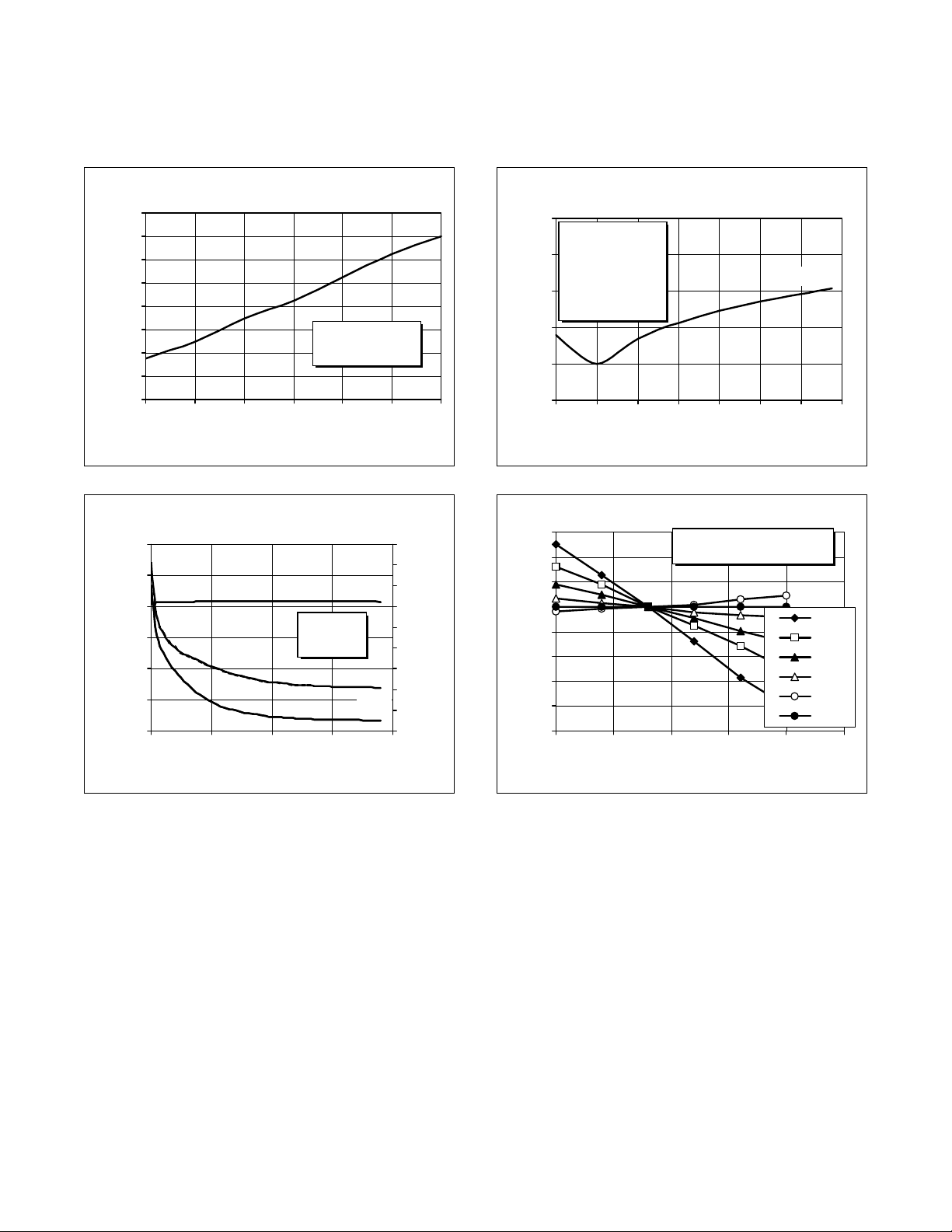
Typical Performance
Typical P
(at P-1dB) , Gain & Efficiency
OUT
vs. Frequency
18
Outp ut Power (W)
16
Gain (dB)
14
Gain
12
Efficiency (%)
10
865 870 875 880 885 890 895
Frequency (MHz)
VDD = 28 V
= 1.5 A Total
I
DQ
225
175
125
75
25
Output Power & Efficiency
Broadband Test Fixture Performance
16
Gain
14
12
Gain (dB)
10
8
865 870 875 880 885 890 895
VDD = 28 V
= 1.5 A Total
I
DQ
= 165 W
P
OUT
Frequency (MHz)
Efficiency (%)
Return
Loss (dB)
60
50
40
30
- 5
20
-10
-15
10
-20
-25
0
Efficiency
Return Loss
2
e
Typical Performance (cont.)
PTF 10161
Output Power vs. Supply Voltage
200
180
160
140
120
100
80
60
Output Power (Watts)
40
18 20 22 24 26 28 30
Supply Voltage (Volts)
Capacitance vs. Supply Volt age
600
500
400
300
200
Cds & Cgs (pF) .
100
C
gs
C
ds
0
0 10203040
Supply Voltage (Volts)
IDQ = 1.5 A Total
f = 894 MHz
(per side)
VGS = 0 V
f = 1 MHz
C
rss
95
85
75
65
55
45
35
25
15
5
*
Crss (pF)
Inter modulation Distortion vs. Output Power
-10
VDD = 28 V
-20
-30
-40
IMD (dBc)
-50
-60
= 1.5 A Total
I
CQ
= 880.0 MHz
f
1
= 880.1 MHz
f
2
30 50 70 90 110 130 150 170
3rd order
Output Power (Watts-PEP)
Gate-Source Volt age vs. Case Temperature
1.03
1.02
1.01
1.00
0.99
0.98
0.97
Bias Voltage (V)
0.96
0.95
-20 5 30 55 80 105
Case Temperature (°C)
Voltage normaliz ed t o 1.0 V
Series show current (A )
1.72
5
8.32
11.6
14.84
18.12
*This part is internally matched. Measurements of the finished
product will not yield these figures.
3
 Loading...