

Ericsson PTF10153 Datasheet
PTF 10153
60 Watts, 1.8–2.0 GHz
GOLDMOS® Field Effect Transistor
Description
The PTF 10153 is an internally matched 60–watt GOLDMOS FET
intended for CDMA and TDMA applications from 1.8 to 2.0 GHz. It
operates with 40% efficiency and 11.5 dB minimum gain. Nitride
surface passivation and full gold metallization ensure excellent device lifetime and reliability.
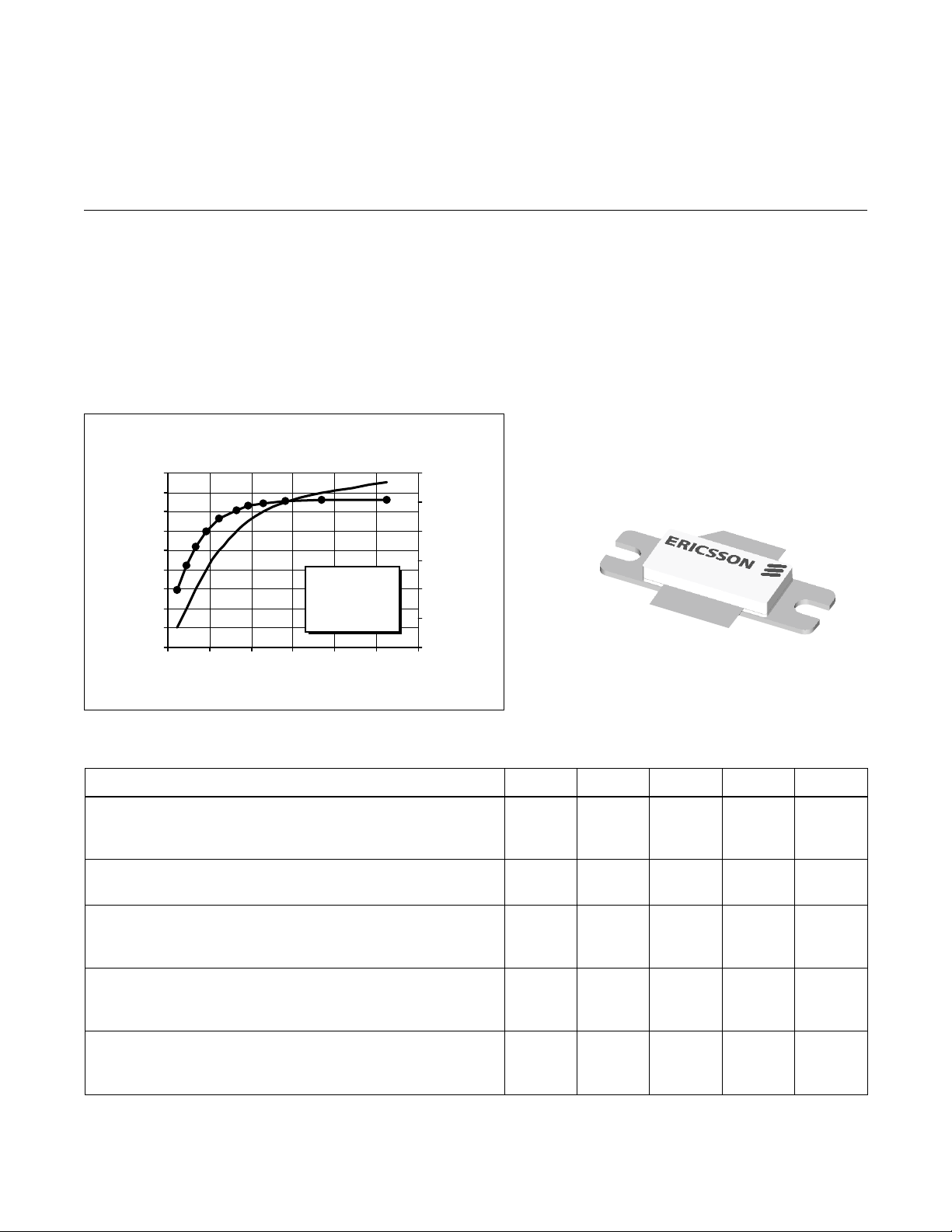
Typical Output Pow er & Efficie ncy
vs. I nput Power
90
80
70
60
50
40
30
20
10
Output Power (Watts)
0
024681012
Inp u t Power (Watts)
VDD = 28 V
= 650mA
I
DQ
f = 188 0 MHz
60
50
40
30
20
Efficiency (%)
10
0
• INTERNALLY MA TCHED
• Guaranteed Performance at 1805, 1843, 1880
MHz, 28 V
- Output Power = 60 Watts Min
- Power Gain = 11.5 dB Min
• Full Gold Metallization
• Silicon Nitride Passivated
• Back Side Common Source
• Excellent Thermal Stability
• 100% Lot Traceability
10153
A-1234569953
Package 20248
RF Specifications (100% T ested)
Characteristic Symbol Min T yp Max Units
Gain
(V
f = 1805, 1843, 1880 MHz)
Power Output at 1 dB Compression
(V
Drain Efficiency
(V
f = 1805, 1843, 1880 MHz)
Return Loss
(V
f = 1805, 1843, 1880 MHz)
Load Mismatch Tolerance
(V
—all phase angles at frequency of test)
All published data at T
= 28 V , P
DD
= 28 V , IDQ = 650 mA, f = 1880 MHz) P-1dB 60 — — Watts
DD
= 28 V , P
DD
= 28 V , P
DD
= 28 V , P
DD
= 60 W, IDQ = 650 mA, G
OUT
= 60 W, IDQ = 650 mA, h
OUT
= 60 W, IDQ = 650 mA, — — — –9.5 dB
OUT
= 60 W, IDQ = 650 mA, f = 1805 Y — — 10:1 —
OUT
= 25°C unless otherwise indicated.
CASE
ps
D
11.5 — — dB
40 — — %
e
1
PTF 10153
e
Electrical Characteristics (100% T ested)
Characteristic Conditions Symbol Min T yp Max Units
Drain-Source Breakdown Voltage VGS = 0 V , ID = 25 mA V
Zero Gate Voltage Drain Current VDS = 28 V , VGS = 0 V I
Gate Threshold Voltage VDS = 10 V , ID = 75 mA V
Forward Transconductance VDS = 10 V , ID = 0.5 A g
(BR)DSS
DSS
GS(th)
fs
65 ——Volts
——1mA
3.0 — 5.0 Volts
1.0 ——Siemens
Maximum Ratings
Parameter Symbol Value Unit
Drain-Source Voltage V
Gate-Source Voltage V
Operating Junction T emperature T
T otal Device Dissipation at P
Above 25°C derate by 1.35 W/°C
Storage T emperature Range T
Thermal Resistance (T
= 70°C) R
CASE
DSS
GS
J
D
STG
qJC
65 Vdc
±20 Vdc
200 °C
237 Watts
–40 to +150 °C
0.74 °C/W
Typical Performance
Typical P
, Gain & Efficiency
OUT
(at P-1dB )
vs. Freque ncy
12
11
10
Gain
9
8
7
1750 1800 1850 1900 1950 2000
Gain (dB)
VDD = 28 V
= 650 mA
I
DQ
F requency (MHz)
Output Pow er (W)
Efficie ncy (%)
90
76
62
48
34
20
Output Power & Efficiency
Broadba n d Test Fix ture Pe rformance
20
Efficiency (%)
16
Gain
12
Gain (dB)
8
4
1800 1820 1840 1860 1880
VDD = 28V
I
= 650 mA
DQ
P
= 60 W
OUT
Return Loss (dB)
F requency (MHz)
60
50
40
- 5
30
-10
20
10
-15
0
-25
Efficiency
Return Loss
2
 Loading...