

Ericsson PTF10149 Datasheet
PTF 10149
70 Watts, 921–960 MHz
GOLDMOS Field Effect Transistor
Description
The PTF 10149 is an internally matched 70–watt GOLDMOS FET
intended for cellular and GSM amplifier applications from 921 to
960 MHz. It operates with 50% efficiency and 16 dB typical gain.
Nitride surface passivation and full gold metallization ensure excellent device lifetime and reliability.
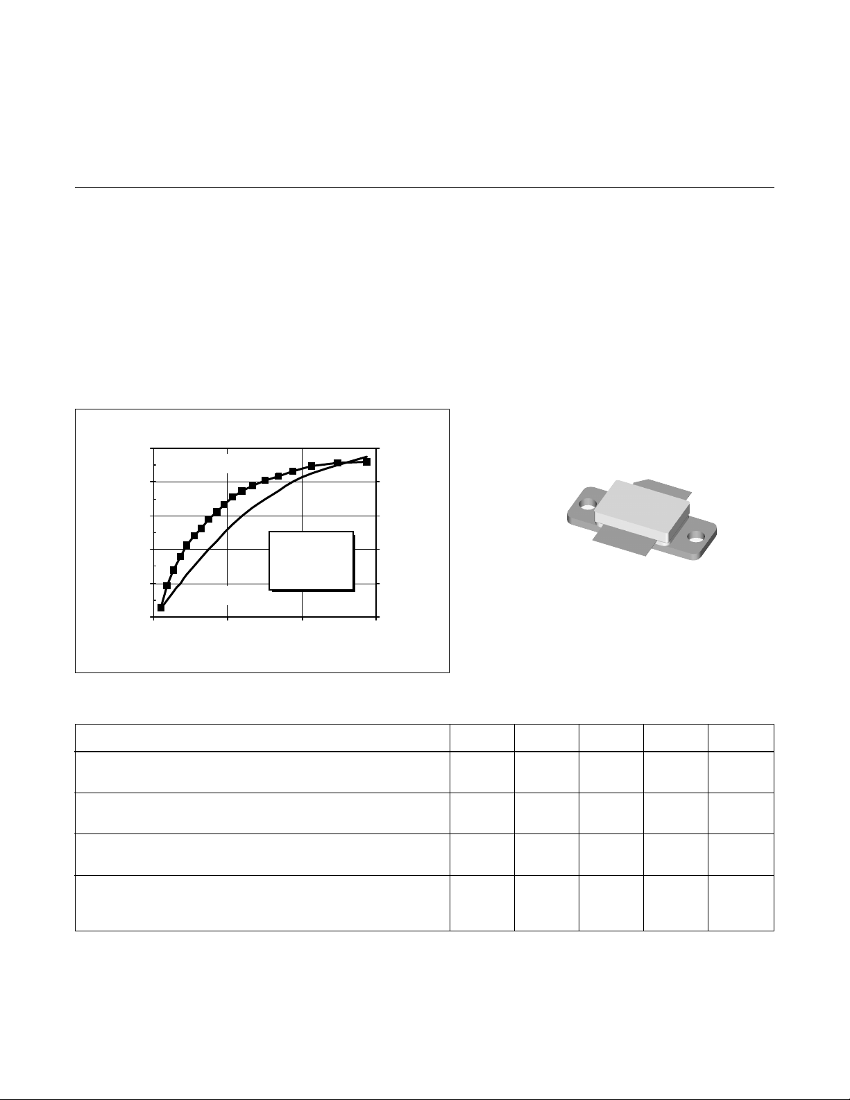
Typical Output Pow er & Efficiency vs. Input Powe r
100
Efficiency
80
60
40
20
Output Power (Watts)
0
Output Pow er
0123
Inp u t Po wer (Watts)
VDD = 26 V
= 750 mA
I
DQ
f = 960 MHz
60
50
40
30
Efficiency (%) x
20
10
• INTERNALLY MATCHED
• Performance at 960 MHz, 26 Volts
- Output Power = 70 Watts
- Power Gain = 16.0 dB Typ
- Efficiency = 50% Typ
• Full Gold Metallization
• Silicon Nitride Passivated
• Excellent Thermal Stability
• 100% Lot Traceability
e
10149
A-1234569935
Package 20252
RF Specifications (100% tested)
Characteristic Symbol Min Typ Max Units
Gain
(V
Power Output at 1 dB Compression
(V
Drain Efficiency
(V
Load Mismatch Tolerance
(V
—all phase angles at frequency of test)
All published data at T
= 26 V, P
DD
= 26 V, IDQ = 750 mA, f = 960 MHz) P-1dB 70 75 — Watts
DD
= 26 V, P
DD
= 26 V, P
DD
= 70 W, IDQ = 750 mA, f = 960 MHz) G
OUT
= 70 W, IDQ = 750 mA, f = 960 MHz) h 47 50 — %
OUT
= 70 W, IDQ = 750 mA, f = 921 MHz Y — — 5:1 —
OUT
= 25°C unless otherwise indicated.
CASE
pe
15.0 16.0 — dB
e
1
PTF 10149
e
Electrical Characteristics (100% Tested)
Characteristic Conditions Symbol Min Typ Max Units
Drain-Source Breakdown Voltage VGS = 0 V, ID = 25 mA V
Drain-Source Leakage Current VDS = 26 V, VGS = 0 V I
Gate Threshold Voltage VDS = 10 V, ID = 75 mA V
Forward Transconductance VDS = 10 V, ID = 3 A g
(BR)DSS
DSS
GS(th)
fs
65 ——Volts
——1.0 mA
3.0 — 5.0 Volts
— 3.0 — Siemens
Maximum Ratings
Parameter Symbol Value Unit
Drain-Source Voltage V
Gate-Source Voltage V
Operating Junction Temperature T
Total Device Dissipation P
Above 25°C derate by 1.12 W/°C
Storage Temperature Range T
Thermal Resistance (T
= 70°C) R
CASE
DSS
GS
J
D
STG
qJC
65 Vdc
±20 Vdc
200 °C
197 Watts
–40 to +150 °C
0.89 °C/W
Typical Performance
Typical P
, Gain & Efficiency
OUT
vs. Frequency
17
Gain (dB)
15
13
VDD = 26 V
= 750 mA
Gain (dB) x
I
11
DQ
9
920 930 940 950 960
F requency (MHz)
O utput Po wer (W)
Efficiency (%)
(at P-1dB )
120
100
80
60
40
Broadba n d Test Fix ture Performance
20
16
Gain
12
Gain (dB)
8
Output Power & Efficiency
4
920 930 940 950 960
Effi ciency (%)
VDD = 26 V
I
= 750 mA
DQ
= 70 W
P
OUT
F requency (MHz)
Return Loss
60
50
40
- 5
30
20
-15
10
-25
0
-35
Efficiency
Return Loss (dB)x
2
 Loading...