

Ericsson PTF10136 Datasheet

PTF 10136
6 Watts, 1.0 GHz
GOLDMOS Field Effect Transistor
Description
The PTF 10136 is a 6–watt GOLDMOS FET intended for large signal
amplifier applications from to 1.0 GHz. It operates at 57% efficiency
with 19 dB typical gain. Nitride surface passivation and full gold
metallization ensure excellent device lifetime and reliability.
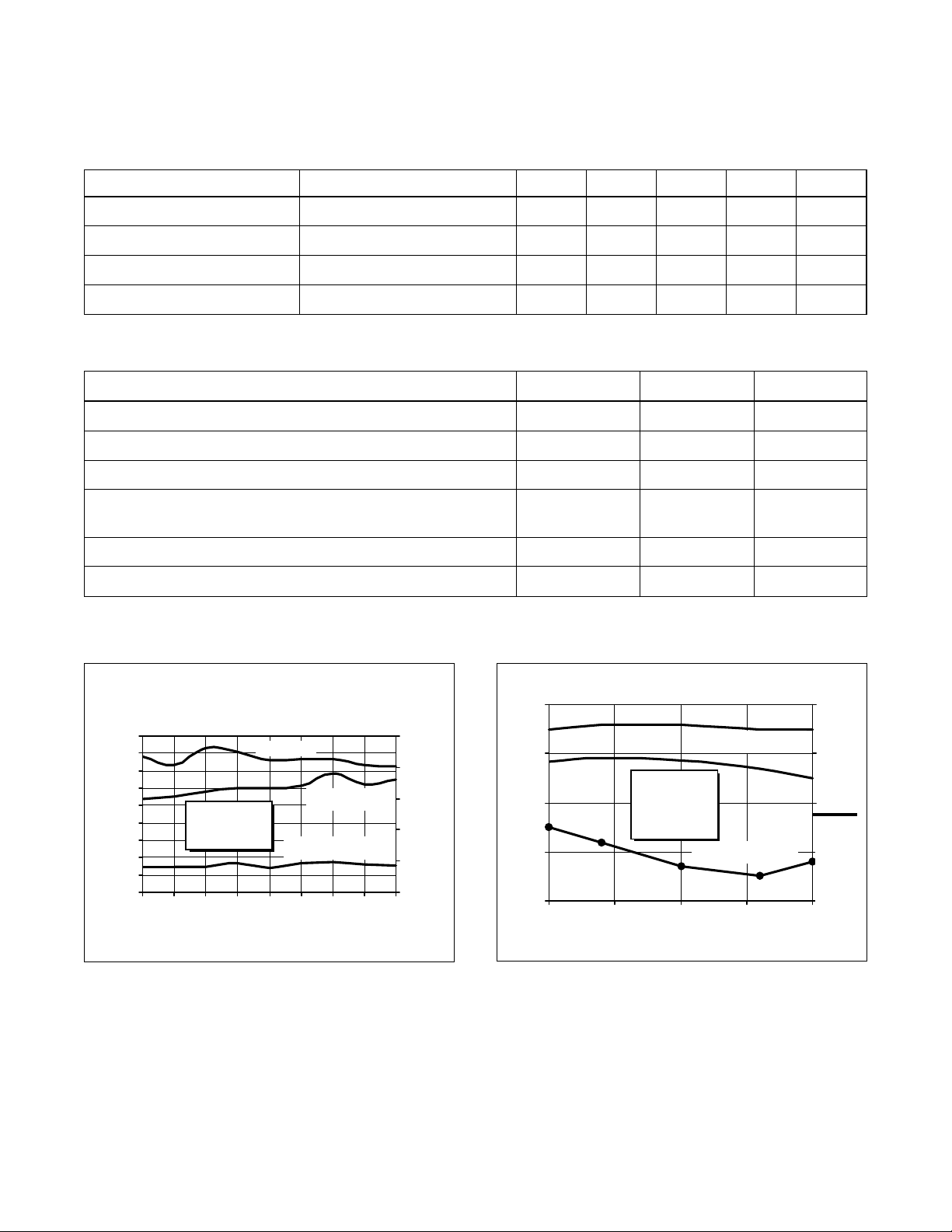
Typical Output Power & Efficiency vs. Input Power
10
8
6
4
2
Output Power (Watts)
Output Pow er
0
0.00 0.05 0.10 0.15
Input Power (Watts)
Efficiency
VDD = 28 V
= 70 mA
I
DQ
f = 960 MH z
70
56
42
28
Efficiency (%) X
14
0
Performance at 960 MHz, 28 Volts
- Output Power = 6 Watts
- Efficiency = 57% Typ
- Power Gain = 19 dB Typ
Full Gold Metallization
Silicon Nitride Passivated
Surface Mountable
Available in T ape and Reel
• 100% Lot Traceability
10136
A-1234569935
Package 20244
RF Specifications (100% Tested)
Characteristic Symbol Min Typ Max Units
Common Source Power Gain
(V
Power Output at 1 dB Compressed
(V
Drain Efficiency
(V
Load Mismatch Tolerance
(V
all phase angles at frequency of test)
All published data at T
= 28 V , P
DD
= 28 V , IDQ = 70 mA, f = 960 MHz) P-1dB 6.0 7.5 — Watts
DD
= 28 V , P
DD
= 28 V , P
DD
= 1 W, IDQ = 70 mA, f = 960 MHz) G
OUT
= 6 W, IDQ = 70 mA, f = 960 MHz) h 50 57 — %
OUT
= 6 W, IDQ = 70 mA, f = 960 MHz— Y — — 10:1 —
OUT
= 25°C unless otherwise indicated.
CASE
ps
18 19 — dB
e
1
PTF 10136
e
Electrical Characteristics (100% T ested)
Characteristic Conditions Symbol Min Typ Max Units
Drain-Source Breakdown Voltage VGS = 0 V , ID = 25 mA V
Drain-Source Leakage Current VDS = 28 V , VGS = 0 V I
Gate Threshold Voltage VDS = 10 V , ID = 75 mA V
Forward Transconductance VDS = 10 V , ID = 0.5 A g
(BR)DSS
DSS
GS(th)
fs
65 ——Volts
——1mA
3.0 — 5.0 Volts
— 0.3 — Siemens
Maximum Ratings
Parameter Symbol Value Unit
Drain-Source Voltage V
Gate-Source Voltage V
Operating Junction Temperature T
Total Device Dissipation P
Above 25°C derate by 0.22 W/°C
Storage Temperature Range T
Thermal Resistance (T
= 70°C) R
CASE
DSS
GS
J
D
STG
qJC
65 Vdc
±20 Vdc
200 °C
39 Watts
–40 to +150 °C
4.5 °C/W
Typical Performance
Typical P
, Gain & Efficiency
OUT
vs. Fre quency
22
20
18
16
14
Gain
12
10
8
6
4
840 860 880 900 920 940 960 980 100
VDD = 28 V
I
= 70 mA
DQ
Gain (dB)
Efficiency (%)
Output Powe r (W)
F requency (MHz)
(at P-1dB )
75
60
45
30
15
0
0
Output Power & Efficiency
Broadba n d Test Fix ture Pe rformance
24
20
Gain (dB)
16
Gain
12
8
960 970 980 990 10 00
VDD = 28 V
I
= 70 mA
DQ
= 6 W
P
OUT
F requency (MHz)
Efficiency (%)
Return Loss (dB)
60
50
40
-8
30
-15
20
-23
Efficiency
Return Loss
2
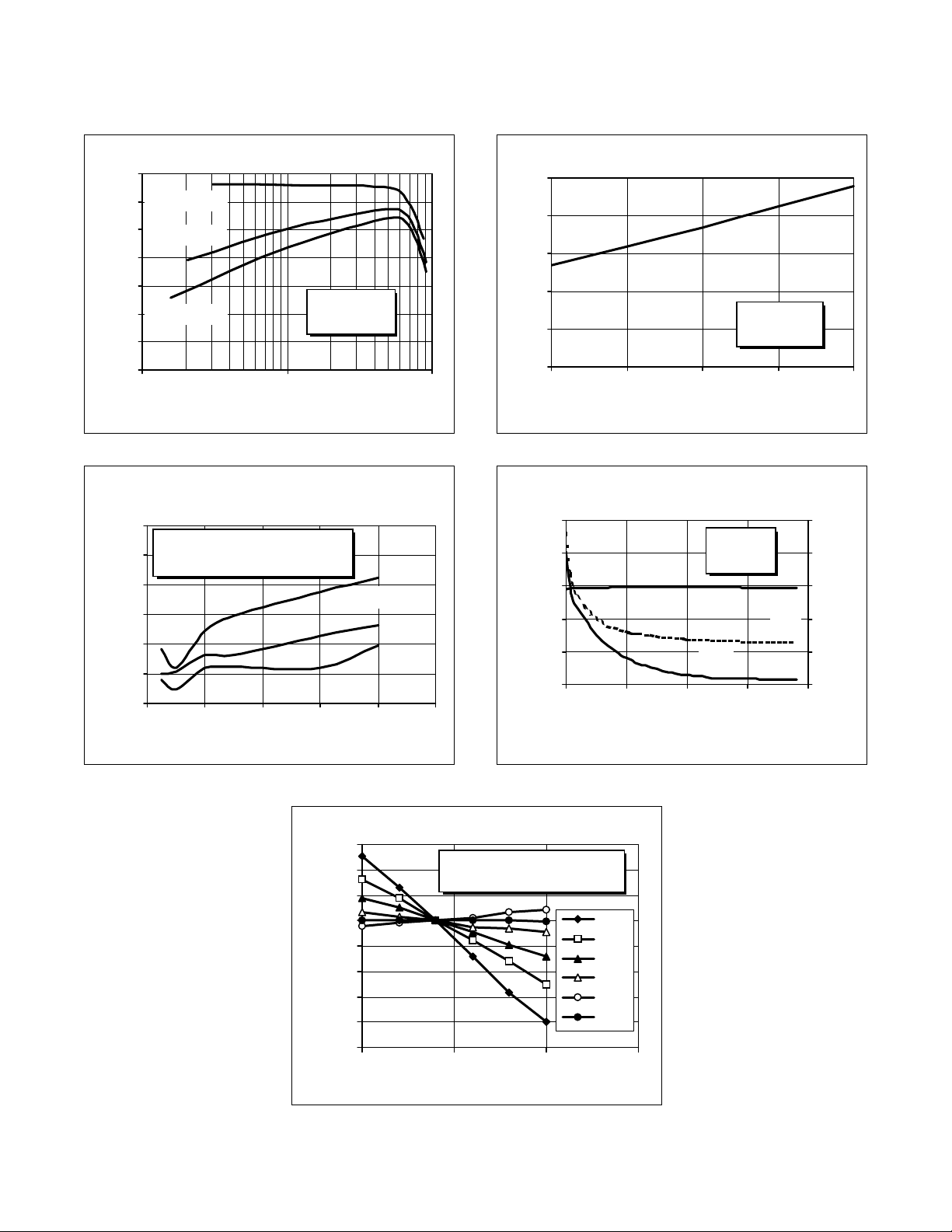
e
PTF 10136
21
IDQ = 70 mA
20
19
IDQ = 35 mA
18
17
IDQ = 20 mA
16
Power Gain (dB)
15
14
0.1 1.0 10.0
VDD = 28 V
f = 960 MHz
Output Power (Watts)
Interm odulation Distortion vs. Output Power
(as measured in a broadb and circu it)
0
VDD = 28 V, IDQ = 70 mA
-10
f
= 960. 0 MHz, f2 = 960.1 MHz
1
Powe r Gain vs. Output Power
-20
-30
IMD (dBc)
-40
-50
-60
0246810
Outp u t P o wer (Watts-PEP )
3rd Order
5th
7th
Output Power vs. Supply Voltage
10
8
6
4
IDQ = 70 mA
2
Output Power (Watts)
0
24 26 28 30 32
f = 960 MHz
Supply Voltage (Volts)
Capa ci tance vs. Suppl y Voltage
20
16
C
12
8
4
Cds and Cgs (pF)
0
0 10203040
gs
Supply Voltage (Volts)
VGS = 0 V
f = 1 MHz
C
rss
C
ds
3.0
2.5
2.0
1.5
1.0
0.5
Crss (pF)
Bias Voltage vs. Temperature
1.03
1.02
1.01
1
0.99
0.98
Bias Voltage (V)
0.97
0.96
0.95
-20 30 80 130
Volt age n or malized to 1.0 V
Series show current (A )
Temp. (°C)
3
0.05
0.145
0.24
0.335
0.43
0.525
 Loading...