

Ericsson PTF10135 Datasheet

PTF 10135
5 Watts, 2.0 GHz
GOLDMOS
™
Field Effect Transistor
Description
The PTF 10135 is a common source N-channel enhancement-mode
lateral MOSFET intended for large signal applications from 1.0 to 2.0
GHz. It is rated at 5 watts minimum output power. Nitride surface
passivation and gold metallization ensure excellent device lifetime
and reliability. 100% lot traceability is standard.
Typical Output Power vs. Input Powe r
8
7
6
5
4
3
2
Output Power (Watts)
1
0
0 0.1 0.2 0.3 0.4 0.5
Inp u t P o wer (Watts)
VDD = 26 V
= 70 mA
I
DQ
f = 200 0 MHz
Guaranteed Performance at 1.99 GHz, 26 V
- Output Power = 5 Watts Min
- Power Gain = 11 dB Min
Gold Metallization
Silicon Nitride Passivated
Back Side Common Source
Excellent Thermal Stability
10135
A-1234569953
Package 20249
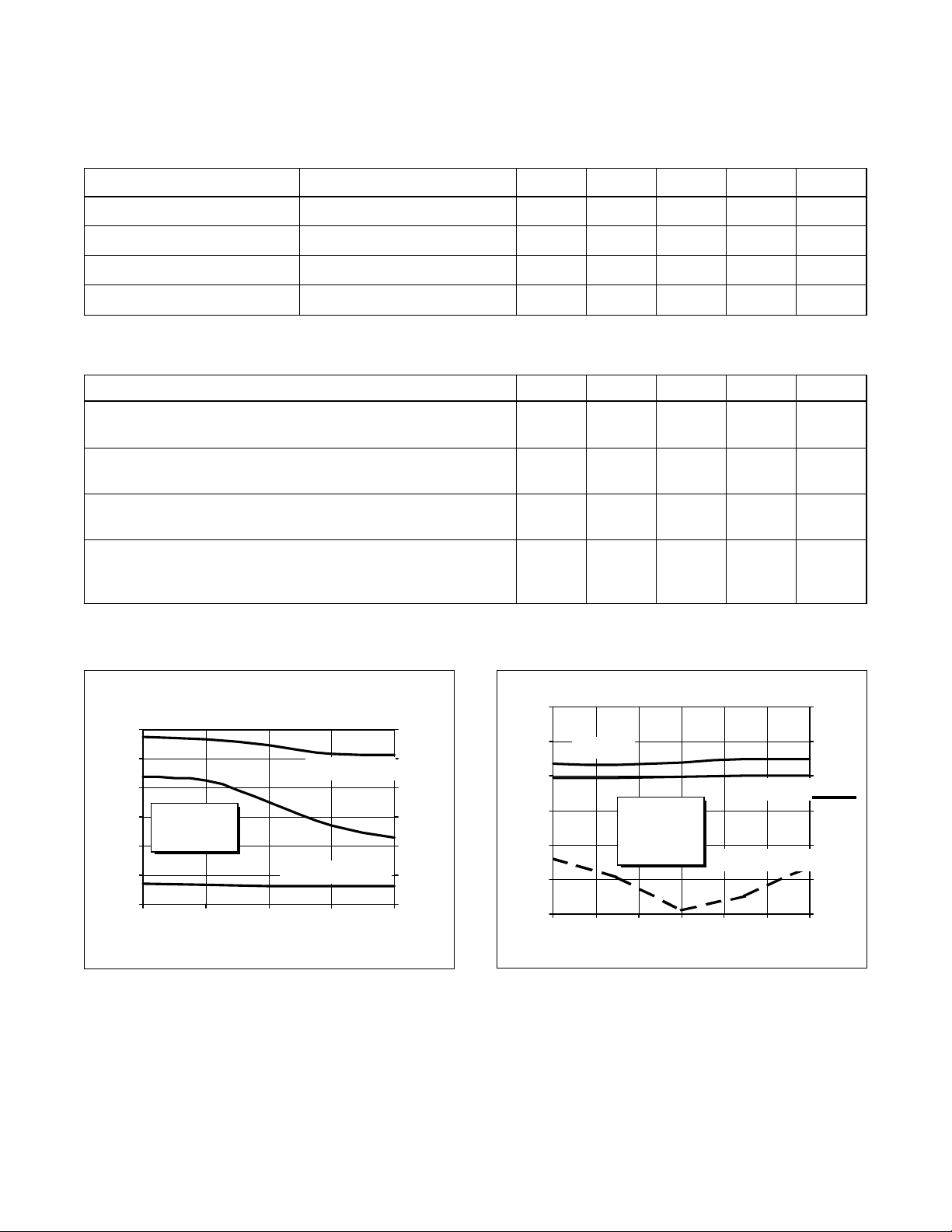
Maximum Ratings
Parameter Symbol Value Unit
Drain-Source Voltage V
Gate-Source Voltage V
Operating Junction Temperature T
Total Device Dissipation at T
Above 25°C derate by 0.22 W/°C
Storage Temperature Range T
Thermal Resistance (T
flange
= 25°C P
flange
= 70°C) R
DSS
GS
J
D
STG
qJC
65 Vdc
±20 Vdc
200 °C
39 Watts
–40 to +150 °C
4.5 °C/W
e
1
PTF 10135
y
)
y
e
Electrical Characteristics (100% T ested)
Characteristic Conditions Symbol Min T yp Max Units
Drain-Source Breakdown Voltage VGS = 0 V , ID = 5 mA V
Zero Gate Voltage Drain Current VDS = 26 V , VGS = 0 V I
Gate Threshold Voltage VDS = 10 V , ID = 75 mA V
Forward Transconductance VDS = 10 V , ID = 2 A g
(BR)DSS
DSS
GS(th)
fs
65 — — V olts
— — 1.0 mA
3.0 — 5.0 Volts
— 0.8 — Siemens
RF Specifications (100% Tested)
Characteristic Symbol Min Typ Max Units
Gain
(V
Power Output at 1 dB Compression
(V
Drain Efficiency
(V
Load Mismatch Tolerance
(V
—all phase angles at frequency of test)
= 26 V , P
DD
= 26 V, IDQ = 70 mA, f = 1.99 GHz) P-1dB 5 — — Watts
DD
= 26 V , P
DD
= 26 V , P
DD
= 1 W, IDQ = 70 mA, f = 1.93, 1.99 GHz) G
OUT
= 5 W, IDQ = 70 mA, f = 1.99 GHz) h
OUT
= 5 W, IDQ = 70 mA, f = 1.99 GHz Y — — 10:1 —
OUT
ps
D
11 — — dB
40 — — %
Typical Performance
Typica l P
, Gain & Efficiency
OUT
vs. Frequency
16
15
Gain (dB)
14
VDD = 26 V
13
Gain
I
= 70 mA
DQ
12
11
10
1700 1800 1900 2000 2100
F requency (MHz)
Effici ency (%)
Output Power (W)
(at P-1d B )
60
50
40
30
20
10
0
Output Power & Efficienc
Broadba n d Test F i xture P erformance
16
14
12
10
Gain (dB
Gain (dB)
Efficiency (%)
VDD = 26 V
= 70 mA
I
8
6
4
1930 1940 1950 1960 1970 1980 1990
P
DQ
OUT
= 4 W
Return Loss (dB)
F requency (MHz)
60
50
40
30
20
10
0
Efficienc
Return Loss
2
 Loading...