

Ericsson PTF10134 Datasheet

PTF 10134
100 Watts, 2.1–2.2 GHz
GOLDMOS® Field Effect Transistor
Description
The PTF 10134 is an internally matched GOLDMOS FET intended
for WCDMA applications from 2.1 to 2.2 GHz. It is rated at 100 watts
power output and operates with 10 dB typical gain. Nitride surface
passivation and gold metallization ensure excellent device lifetime
and reliability.
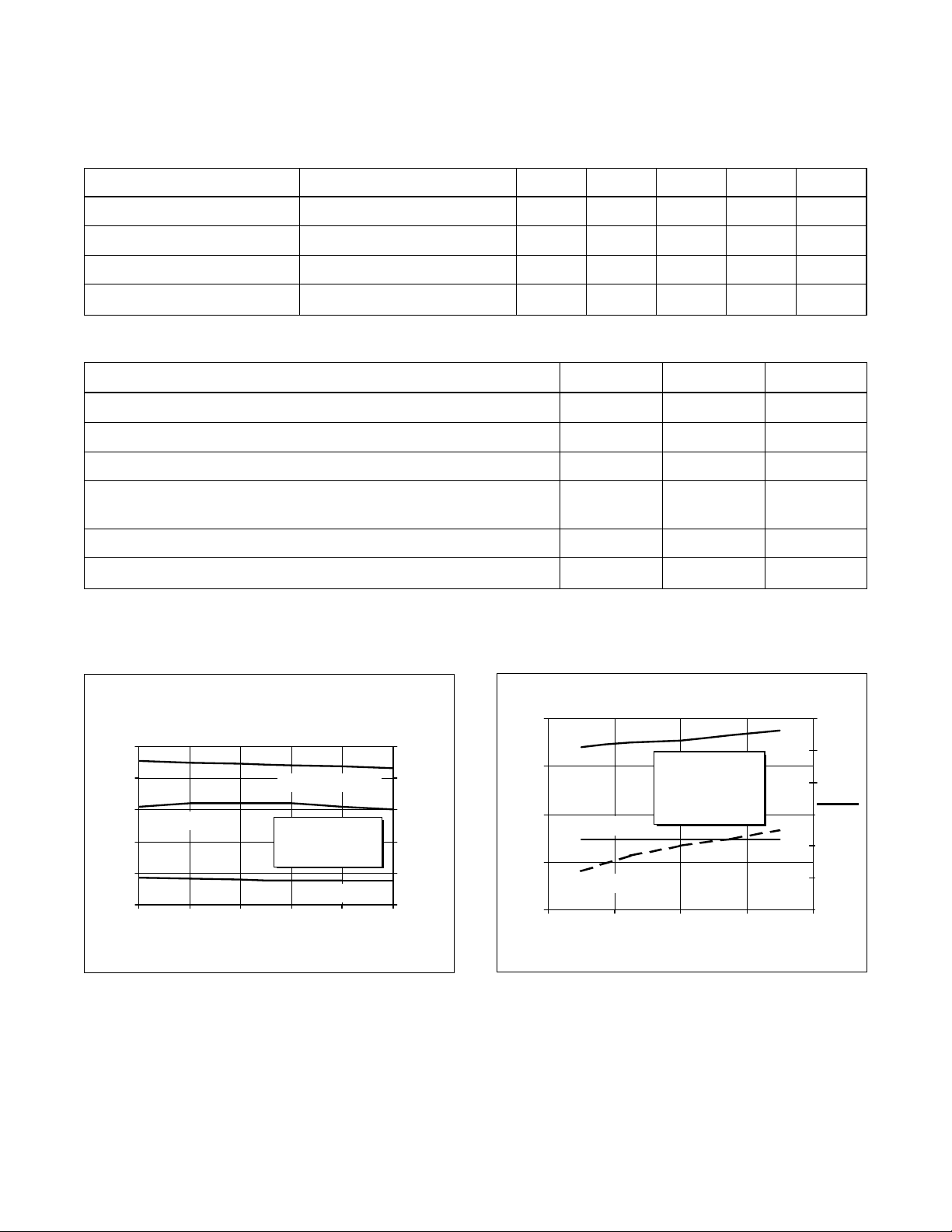
Typical Output Power & Efficiency vs. Input Power
120
Output Power
100
48
40
• INTERNALLY MATCHED
• Guaranteed Performance at 2.17 GHz, 28 V
- Output Power = 100 Watts Min
- Power Gain = 10 dB Typ
• Full Gold Metallization
• Excellent Thermal Stability
• 100% Lot Traceability
80
60
40
20
Output Power (Watts)
0
02468101214
Input Po wer (Watts )
VDD = 28 V
I
DQ
f = 2170 M H z
Efficiency
= 1.3 A Total
32
24
16
Efficiency (%) X
8
0
10134
1234569953A
Package 20250
RF Specifications (100% Tested)
Characteristic Symbol Min T yp Max Units
Gain
(V
Power Output at 1.5 dB Compression
(V
Drain Efficiency
(V
Load Mismatch Tolerance
(V
—all phase angles at frequency of test)
All published data at T
= 28 V, P
DD
= 28 V, IDQ = 1.3 A Total, f = 2.17 GHz) P-1dB 100 — — Watts
DD
= 28 V, P
DD
= 28 V, P
DD
= 30 W, IDQ = 1.3 A Total, f = 2.17 GHz) G
OUT
= 100 W, IDQ = 1.3 A Total, f = 2.17 GHz) h
OUT
= 80 W, IDQ = 1.3 A Total, f = 2.17 GHz Y — — 10:1 —
OUT
= 25°C unless otherwise indicated.
CASE
ps
D
9.5 10 — dB
—37—%
e
1
PTF 10134
e
Electrical Characteristics (100% Tested—characteristics, conditions and limits shown per side)
Characteristic (per side) Conditions Symbol Min Typ Max Units
Drain-Source Breakdown Voltage VGS = 0 V, ID = 100 mA V
(BR)DSS
Zero Gate Voltage Drain Current VDS = 28 V, VGS = 0 V I
Gate Threshold Voltage VDS = 10 V, ID = 150 mA V
Forward Transconductance VDS = 10 V, ID = 2 A g
DSS
GS(th)
fs
65 ——Volts
——5.0 mA
3.0 — 5.0 Volts
— 4.0 — Siemens
Maximum Ratings
Parameter Symbol Value Unit
Drain-Source Voltage
Gate-Source Voltage
Operating Junction Temperature T
Total Device Dissipation P
Above 25°C derate by 2.51 W/°C
Storage Temperature Range T
Thermal Resistance (T
(1)
per side
(1)
(1)
CASE
V
V
= 70°C) R
DSS
GS
J
D
STG
qJC
–40 to +150 °C
65 Vdc
±20 Vdc
200 °C
440 Watts
0.39 °C/W
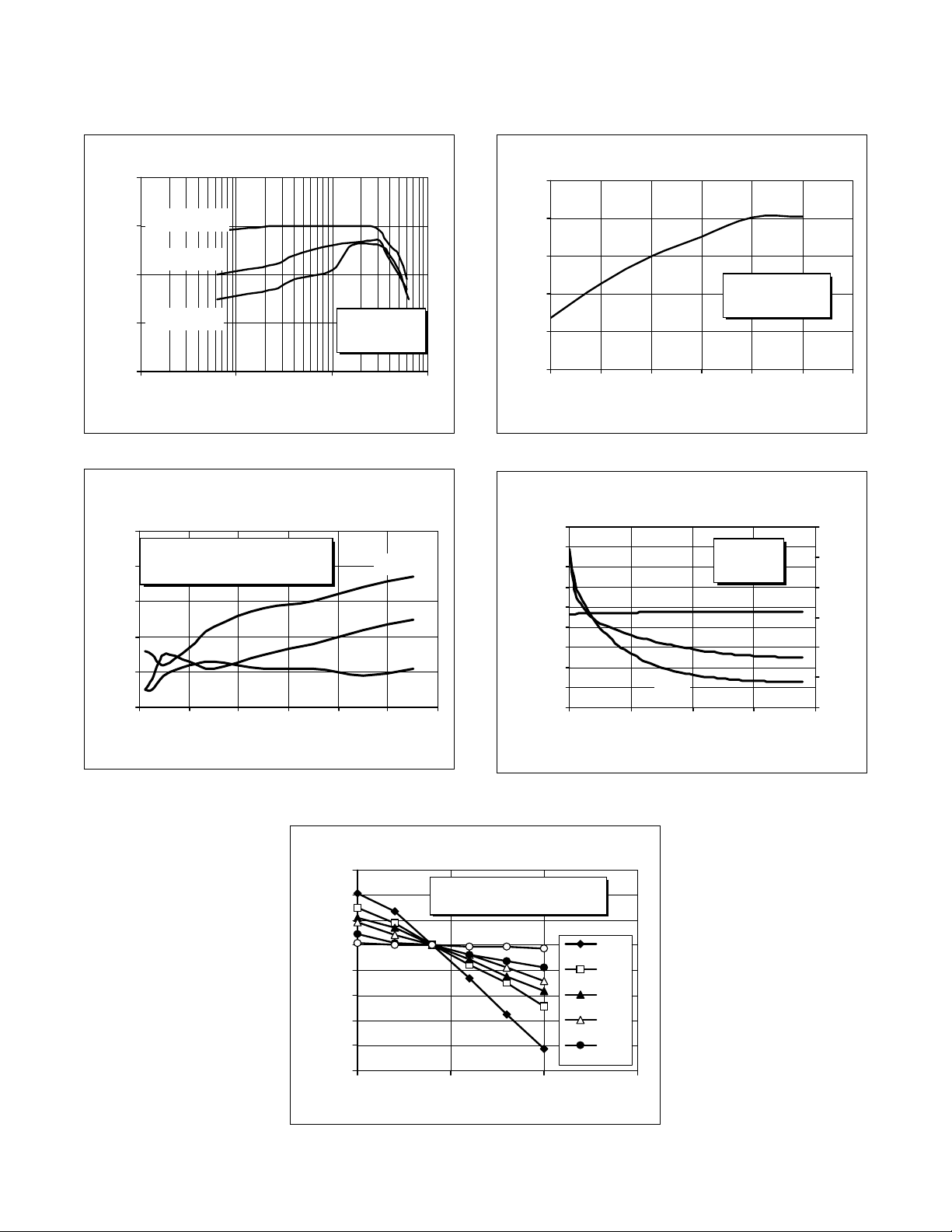
Typical Performance
Typical P
, Gain & Efficiency
OUT
(at P-1dB)
vs. Frequency
12
11
10
Gain (dB)
Gain
9
8
7
2100 2120 2140 2160 2180 2200
Frequency (MHz)
Out p ut Power (W)
VDD = 28 V
= 1.3 A Total
I
DQ
Efficiency (%)
120
100
80
60
40
20
Output Power & Efficiency
Gain (dB)
Broadband Test Fixture Per formance
11
Gain
9
7
Efficiency
5
Return Loss
3
2100 2120 2140 2160 2180
VDD = 28 V
I
= 1.3 A Total
DQ
P
= 25 W
OUT
Frequency (MHz)
60
50
40
30
- 5
20
-15
-25
10
-35
0
Efficiency (%)Return Loss (dB)
2
e
C
C
PTF 10134
11
IDQ = 1300 mA
10
IDQ = 650 mA
9
IDQ = 325 mA
8
Power Gain (dB)
7
0.1 1.0 10.0 100.0
VDD = 28 V
f = 2170 MHz
Output Power (Watts)
Intermodul ation Distortion vs. Output Powe r
(as measured i n a bro adban d circu it)
-15
Power Gain vs. Out put Power
VDD = 28 V, IDQ = 1.3 A Total
-25
f
= 2169 MHz, f2 = 2170 MHz
1
-35
-45
IMD (dBc)
-55
-65
0 20 40 60 80 100 120
Outp ut Po wer (Watts-PEP)
3rd Order
5th
7th
Output Power vs. Supply Voltage
65
60
55
50
IDQ = 1.3 A Total
f = 2170 MHz
45
Output Power (Watts)
40
24 26 28 30 32 34 36
Supply Voltage (Volts)
Capa cita nce vs. Supply Vol ta ge *
450
400
350
300
250
200
150
100
Cds and Cgs (pF)
50
0
010203040
Supply Voltage (Volts)
gs
C
rss
VGS = 0 V
f = 1 MHz
ds
30
25
20
15
10
5
0
Crss
* This part is internally matched. Measurements of the finished
product will not yield these results.
Bias Voltage vs. T emperatur e
1.03
1.02
1.01
1.00
0.99
0.98
Bias Voltage (V)
0.97
0.96
0.95
-20 30 80 130
Voltage normalized to 1.0 V
Series show current (A)
0.800
2.767
4.733
6.700
8.667
Temp. (°C)
3
 Loading...