

Ericsson PTF10133 Datasheet

PTF 10133
)
85 Watts, 860–960 MHz
GOLDMOS
™
Field Effect T ransistor
Description
The PTF 10133 is an internally matched 85 watt LDMOS FET
intended for cellular, GSM and D-AMPS applications. This device
operates at 50% efficiency with 13.5 dB of gain. Full gold metallization
ensures excellent device lifetime and reliability.
Typical Output Power vs. Input Pow er
120
100
80
60
40
20
Output Power (Watts)
0
Output Power
0123456
Input Power (Watts)
Efficiency
VDD = 28.0 V
I
= 1.0 A
DQ
f = 894 MHz
60
50
40
30
20
10
0
Efficiency (%
INTERNALLY MA TCHED
•
• Performance at 894 MHz, 28 Volts
- Output Power = 85 Watts
- Power Gain = 13.5 dB Typ
- Efficiency = 50% Typ
• Full Gold Metallization
• Silicon Nitride Passivated
• Excellent Thermal Stability
• 100% Lot Traceability
10133
A-1234569947
Package 20248
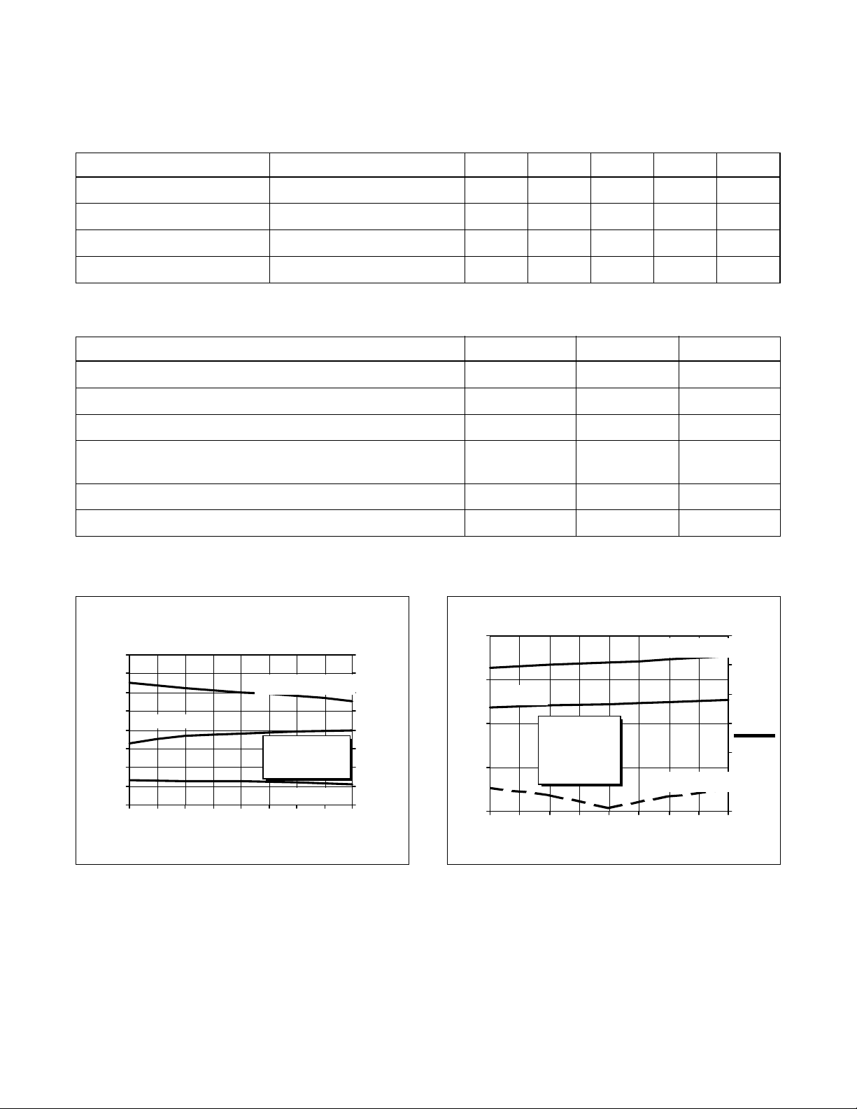
RF Specifications (100% T ested)
Characteristic Symbol Min T yp Max Units
Gain
(V
Power Output at 1 dB Compression
(V
Drain Efficiency
(V
Load Mismatch Tolerance
(V
—all phase angles at frequency of test)
All published data at T
= 28 V , P
DD
= 28 V , IDQ = 1.0 A, f = 894 MHz) P-1dB 85 90 — Watts
DD
= 28 V , P
DD
= 28 V , P
DD
= 85 W, IDQ = 1.0 A, f = 894 MHz) G
OUT
= 85 W, IDQ = 1.0 A, f = 894 MHz) h 45 50 — %
OUT
= 85 W, IDQ = 1.0 A, f = 894 MHz Y — — 10:1 —
OUT
= 25°C unless otherwise indicated.
CASE
ps
12.5 13.5 — dB
e
1
PTF 10133
y
)
y
s
e
Electrical Characteristics (100% T ested)
Characteristic Conditions Symbol Min Typ Ma x Units
Drain-Source Breakdown Voltage VGS = 0 V , ID = 25 mA V
Drain-Source Leakage Current VDS = 28 V , VGS = 0 V I
Gate Threshold Voltage VDS = 10 V , ID = 75 mA V
Forward Transconductance VDS = 10 V , ID = 3 A g
(BR)DSS
DSS
GS(th)
fs
65 — — Volts
— — 1.0 mA
3.0 — 5.0 Volts
— 3.0 — Siemens
Maximum Ratings
Parameter Symbol Value Unit
Drain-Source Voltage V
Gate-Source Voltage V
Operating Junction T emperature T
T otal Device Dissipation P
Above 25°C derate by 1.18 W/°C
Storage T emperature Range T
Thermal Resistance (T
= 70°C) R
CASE
DSS
GS
J
D
STG
qJC
65 Vdc
±20 Vdc
200 °C
205 Watts
–40 to +150 °C
0.85 °C/W
Typical Performance
Typical P
18
17
16
15
14
Gain
13
12
11
10
860 865 870 875 880 885 890 895 900
, Gain & Effici ency (at P-1dB )
OUT
vs. Frequency
Out put Pow er (W)
Gain
VDD = 28 V
= 1.0 A
I
DQ
Efficiency
F requency (MHz)
120
110
100
90
80
70
60
50
40
Output Power & Efficienc
Broadba n d Test Fix ture Performa nce
20
16
Gain (dB)
12
Gain (dB
8
4
860 865 870 875 880 885 890 895 900
VDD = 28 V
I
= 1. 0 A
DQ
P
= 85 W
OUT
F requency (MHz)
Effici ency (%)
Return Loss (dB)
60
50
40
30
20
0
10
-10
0
-20
Efficienc
Return Los
2
 Loading...