

Ericsson PTF10100 Datasheet
e
)
165 Watts, 860–900 MHz
LDMOS Field Effect Transistor
Description
The 10100 is an internally matched common source N-channel
enhancement-mode lateral MOSFET intended for large signal amplifier
applications from 860 to 900 MHz. It is rated at 165 watts power output.
Nitride surface passivation and gold metallization ensure excellent
device lifetime and reliability.
PTF 10100
•
INTERNALLY MA TCHED
• Performance at 894 MHz, 28 Volts
- Output Power = 165 Watts
- Power Gain = 13.0 dB Typ
- Drain Efficiency = 50% T yp
• Full Gold Metallization
• Silicon Nitride Passivated
• Back Side Common Source
• 100% lot traceability
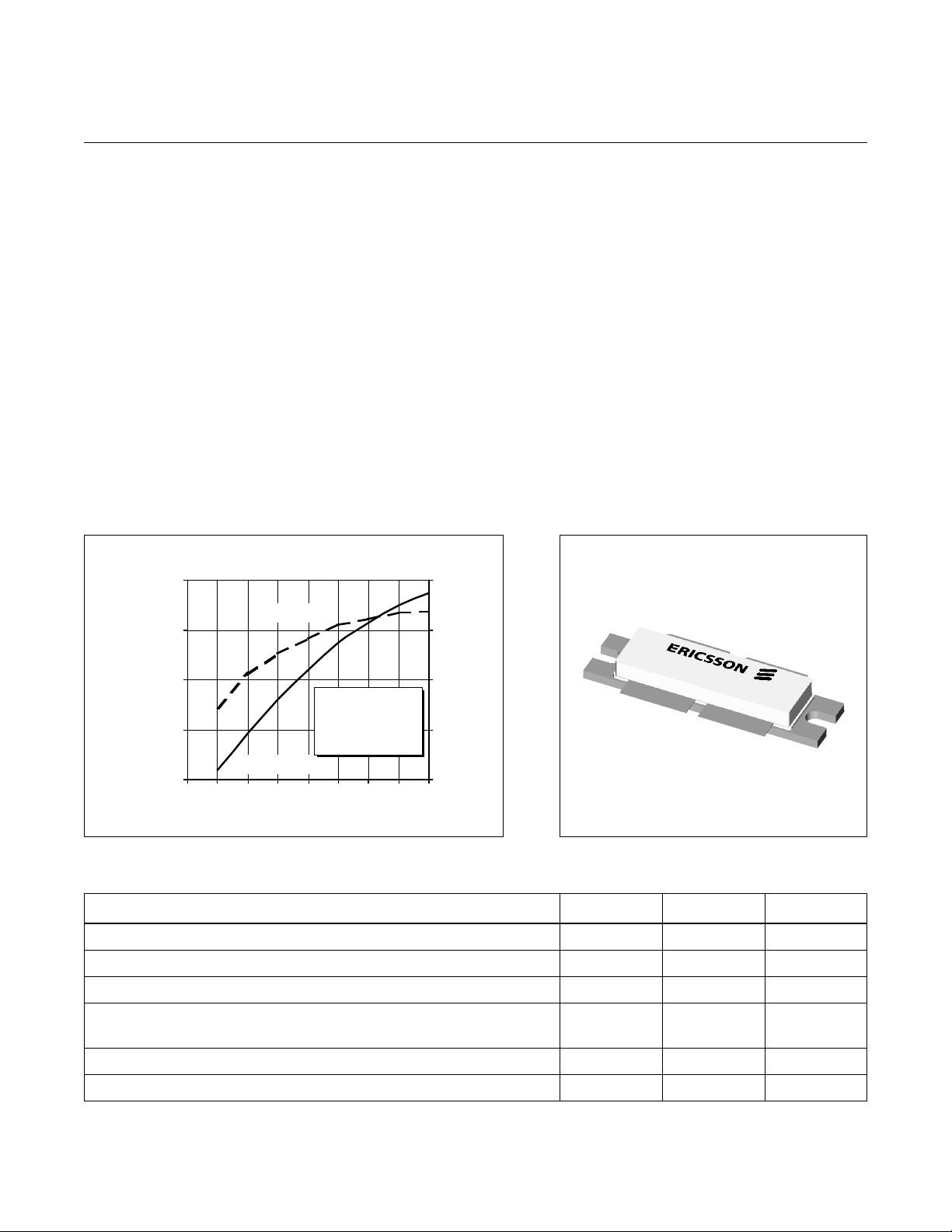
Typical Output Pow er & Efficiency vs. Input Power
180
Efficiency
140
100
VDD = 28.0 V
= 1.8 A Tota l
I
60
Output Power (Watts)
Output Power
20
012345678
Input Power (Watts)
DQ
f = 880 MHz
60
45
30
Efficiency (%
15
0
10100
A-1234569917
Package 20250
Maximum Ratings
Parameter Symbol Value Unit
Drain-Source Voltage
Gate-Source Voltage
Operating Junction T emperature T
T otal Device Dissipation at T
Above 25°C derate by 2.85 W/°C
Storage T emperature Range T
Thermal Resistance (T
(1)
per side
(1)
(1)
flange
= 25°C P
flange
= 70°C) R
V
DSS
V
STG
GS
J
D
qJC
65 Vdc
±20 Vdc
200 °C
500 Watts
–40 to +150 °C
0.35 °C/W
1

PTF 10100
y
s
y
e
Electrical Characteristics (per side) (100% T ested)
Characteristic Conditions Symbol Min T yp Max Units
Drain-Source Breakdown Voltage VGS = 0 V , ID = 5 mA V
(BR)DSS
Drain-Source Leakage Current VDS = 28 V , VGS = 0 V I
Gate Threshold Voltage VDS = 10 V , ID = 75 mA V
Forward Transconductance VDS = 10 V , ID = 3 A g
DSS
GS(th)
fs
65 — — Volts
— — 1.0 mA
— 4.3 — Volts
— 2.5 — Siemens
RF Specifications (100% T ested)
Characteristic Symbol Min T yp Max Units
Gain
(V
Power Output at 1 dB Compression
(V
Drain Efficiency
(V
Load Mismatch Tolerance
(V
f = 893.9, 894 MHz—all phase angles at frequency of test)
= 28 V , P
DD
= 28 V , ICQ = 1.8 A Total, f = 880 MHz) P-1dB 165 180 — Watts
DD
= 28 V , P
DD
= 28 V , P
DD
= 165 W, IDQ = 1.8 A Total, f = 894 MHz) G
OUT
= 165 W, IDQ = 1.8 A Total, f = 894 MHz) h 45 50 — %
OUT
= 165 W(PEP), IDQ = 1.8 A Total, Y — — 10:1 —
OUT
ps
12.0 13.0 — dB
Typical Performance
Typical P
18
16
14
Gain
Gain (dB)
12
10
865 870 875 880 885 890 895
(at P- 1dB) , Gain vs. Frequency
OUT
Out pu t Power (W)
VDD = 28 V
= 1.8 A Total
I
DQ
Efficiency (%)
Frequency (MHz)
225
175
125
75
Output Power & Efficienc
25
Broadband Test Fixture Performance
16
Efficiency (%)
14
Gain
12
Gain (dB)
10
8
865 870 875 880 885 890 895
VDD = 28 V
= 1.8 A Tota l
I
DQ
= 165 W
P
OUT
Frequency (MHz)
Return
Loss (dB)
60
50
40
30
- 5
20
-10
10
-15
-20
0
-25
Efficienc
Return Los
2
 Loading...