

Ericsson PTF10065 Datasheet
PTF 10065
30 Watts, 1.93–1.99 GHz
GOLDMOS® Field Effect Transistor
Description
The PTF 10065 is a 30–watt GOLDMOS FET intended for PCS
amplifier applications from 1.93 to 1.99 GHz. It typically operates with
11 dB gain. Nitride surface passivation and full gold metallization
ensure excellent device lifetime and reliability.
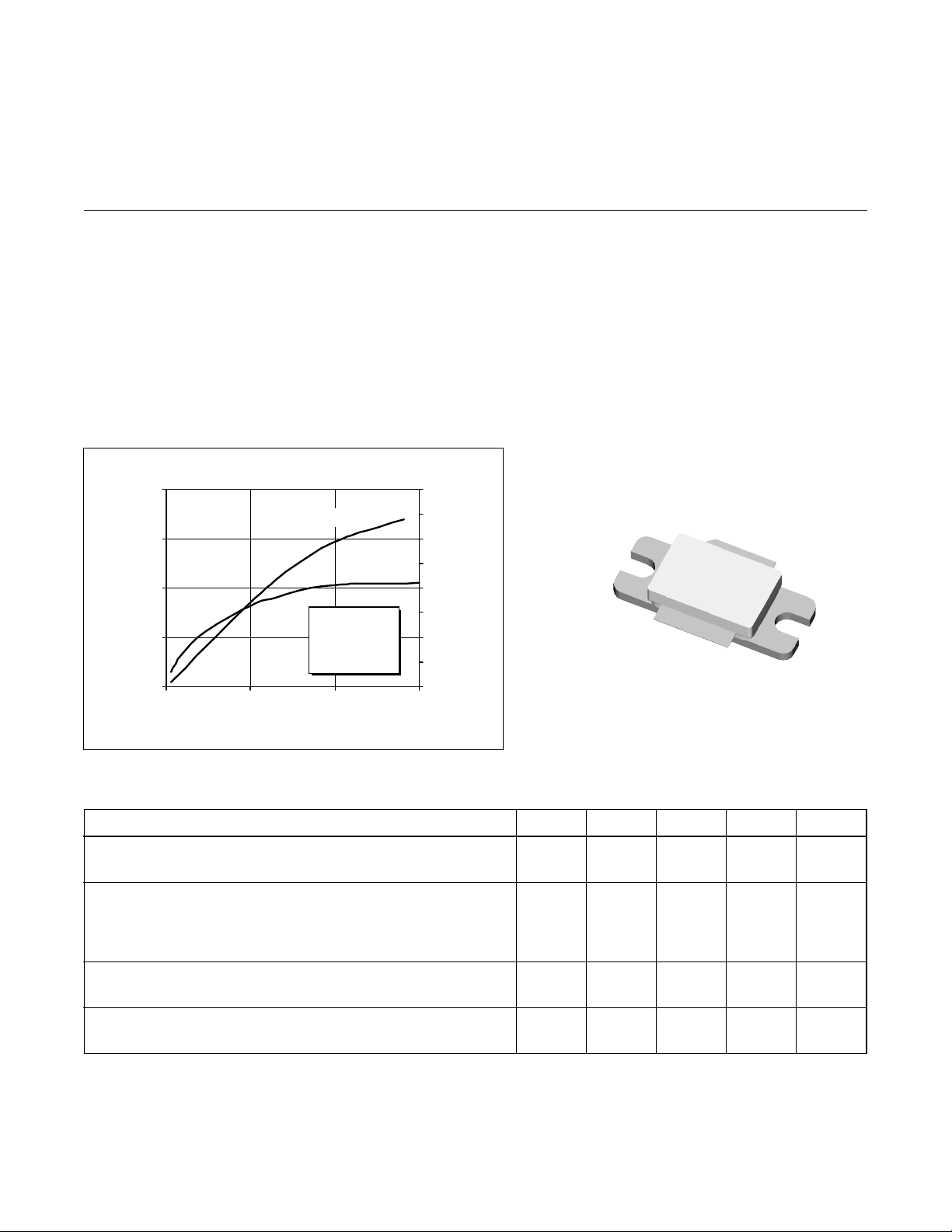
Output Pow er and Efficiency vs. Input Power
40
Output P ower
30
Efficiency
20
VDD = 28 V
10
Output Power (Watts)
0
0123
Input Power (Watts)
= 380 mA
I
DQ
f = 1.99 GHz
80
70
60
50
40
30
20
10
0
Efficiency
• INTERNALLY MATCHED
• Guaranteed Performance at 1.99 GHz, 28 V
- Output Power = 30 Watts Min
- Power Gain = 11.0 dB Typ
• Full Gold Metallization
• Silicon Nitride Passivated
• Excellent Thermal Stability
• 100% Lot Traceability
e
10065
1234569921A
Package 20237
RF Specifications (100% Tested)
Characteristic Symbol Min Typ Max Units
Gain
(V
ACPR (40 Walsh Codes)
(V
(VDD = 28 V, P
Gain Flatness
(V
Drain Efficiency
(V
All published data at T
= 28 V, P
DD
= 28 V, P
DD
= 28 V, P
DD
= 28 V, P
DD
= 3 W, IDQ = 380 mA, f = 1.93, 1.99 GHz) G
OUT
= 3 W(CDMA), IDQ = 380 mA, f = 1.99 GHz) ACPR - 50 — — dBc
OUT
= 3 W(CDMA), IDQ = 380 mA, f = 1.99 GHz) ACPR - 62 — — dBc
OUT
= 3 W, IDQ = 380 mA, f = 1.930–1.990 GHz) GDf — — 0.7 dB
OUT
= 3 W, IDQ = 380 mA, f = 1.99 GHz) h
OUT
= 25°C unless otherwise indicated.
CASE
ps
±885 KHz
±1.98 MHz
D
— 11.0 — dB
9——%
(table continues next page)
e
1
PTF 10065
e
RF Specifications (cont.) (100% Tested)
Characteristic Symbol Min Typ Max Units
Power Output at 1 dB Compressed
(V
Load Mismatch Tolerance
(V
f = 1.99 GHz—all phase angles at frequency of test)
Input Return Loss
(V
Insertion Phase (Referenced to Correlation Devices)
(V
= 28 V, IDQ = 380 mA, f = 1.99 GHz) P-1dB 30 ——Watts
DD
= 28 V, P
DD
= 28 V, P
DD
= 28 V, P
DD
= 30 W, IDQ = 380 mA, Y ——10:1 —
OUT
= 3 W, IDQ = 380 mA, f = 1.93, 1.99 GHz) Rtn Loss 10 ——dB
OUT
= 3 W, IDQ = 380 mA, f = 1.96 GHz) f –10 — +10 Deg.
OUT
Electrical Characteristics (cont.) (100% Tested) (100% Tested)
Characteristic Conditions Symbol Min Typ Max Units
Drain-Source Breakdown Voltage VGS = 0 V, ID = 25 mA V
Zero Gate Voltage Drain Current VDS = 28 V, VGS = 0 V I
Gate Threshold Voltage VDS = 10 V, ID = 75 mA V
Forward Transconductance VDS = 10 V, ID = 6 A g
Gate-Source Leakage VGS = 10 V I
Gate Quiescent Voltage VDS = 28 V, ID = 380 mA V
(BR)DSS
DSS
GS(th)
fs
GSsf
GS(q)
62 ——Volts
——1.0 mA
— 3.8 — Volts
— 1.8 — Siemens
——1 mA
3.0 — 5.0 V
Maximum Ratings
Parameter Symbol Value Unit
Drain-Source Voltage V
Gate-Source Voltage V
Operating Junction Temperature T
Total Device Dissipation P
Above 25°C derate by 0.7 W/°C
Storage Temperature Range T
Thermal Resistance (T
= 70°C) R
CASE
DSS
GS
J
D
STG
qJC
62 Vdc
±20 Vdc
200 °C
120 Watts
–40 to +150 °C
1.4 °C/W
2
 Loading...