

Ericsson PTF10052 Datasheet
PTF 10052
35 Watts, 1.0 GHz
GOLDMOS
™
Field Effect T ransistor
Description
The PTF 10052 is a 35 Watt LDMOS FET intended for large signal
amplifier applications to 1.0 GHz. It operates at 55% efficiency and
13.5 dB of gain. Nitride surface passivation and full gold metallization
ensure excellent device lifetime and reliability.
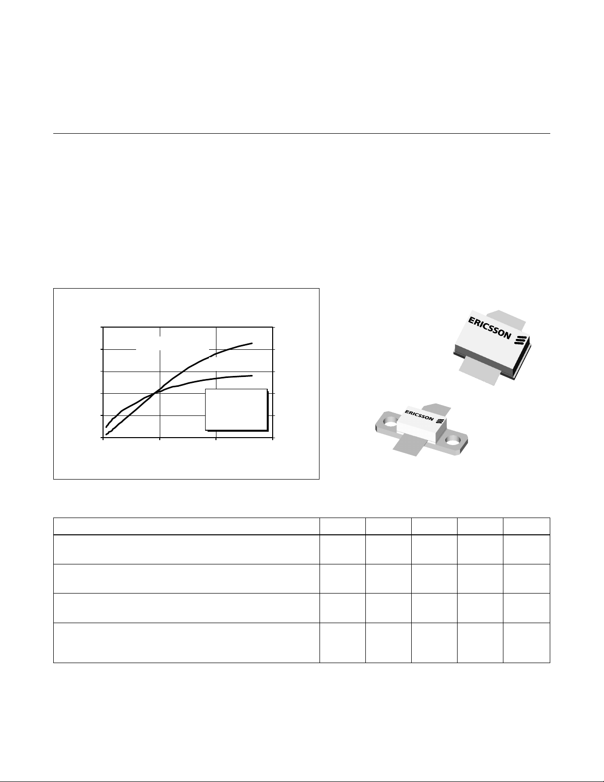
Typi cal O u tpu t P o wer & Efficie n cy
vs. Input Powe r
50
40
30
20
Output Power
10
0
0123
Output Power (W)
VDD = 28 V
I
f = 960 MHz
Input Power (Watts)
Efficiency (%)
= 300 mA
DQ
100
80
60
40
20
0
Efficiency
• Performance at 960 MHz, 28 Volts
- Output Power = 35 Watts
- Power Gain = 13.5 dB Typ
- Efficiency = 55% Typ
• Full Gold Metallization
• Silicon Nitride Passivated
• Back Side Common Source
• 100% Lot Traceability
• Available in Package 20222 as PTF 10007
Package
20235
10007
A-1234569725
10052
B-1234569916
Package
20222
RF Specifications (100% Tested)
Characteristic Symbol Min Typ Max Units
Gain
(V
Power Output at 1 dB Compression
(V
Drain Efficiency
(V
Load Mismatch Tolerance
(V
all phase angles at frequency of test)
All published data at T
= 28 V, P
DD
= 28 V, IDQ = 300 mA, f = 960 MHz) P-1dB 35 — — Watts
DD
= 28 V, P
DD
= 28 V, P
DD
= 35 W, IDQ = 300 mA, f = 960 MHz) G
OUT
= 35 W, IDQ = 300 mA, f = 960 MHz) h 50 55 — %
OUT
= 35 W, IDQ = 300 mA, f = 960 MHz— Y — — 10:1 —
OUT
= 25°C unless otherwise indicated.
CASE
ps
12.0 13.5 — dB
e
1
PTF 10052
y
)
y
s
e
Electrical Characteristics (100% Tested)
Characteristic Conditions Symbol Min Typ Max Units
Drain-Source Breakdown Voltage VGS = 0 V , ID = 5 mA V
Drain-Source Leakage Current VDS = 28 V , VGS = 0 V I
Gate Threshold Voltage VDS = 10 V , ID = 75 mA V
Forward Transconductance VDS = 10 V , ID = 3 A g
(BR)DSS
DSS
GS(th)
fs
65 70 — V olts
— — 1.0 mA
3.0 — 5.0 Volts
— 2.8 — Siemens
Maximum Ratings
Parameter Symbol Value Unit
Drain-Source Voltage V
Gate-Source Voltage V
Operating Junction Temperature T
Total Device Dissipation P
Above 25°C derate by 0.7 W/°C
Storage Temperature Range T
Thermal Resistance (T
= 70°C) R
CASE
DSS
GS
J
D
STG
qJC
60 Vdc
±20 Vdc
200 °C
120 Watts
–40 to +150 °C
1.4 °C/W
Typical Performance
P
, Gain & Efficiency
OUT
30
25
20
Gain (dB)
15
Gain
10
VDD = 28 V
5
I
= 300 mA
DQ
0
400 500 600 700 800 900 1000
(at P-1dB)
Frequ ency ( M Hz)
vs. Frequency
Effici ency (%)
O utpu t Po wer (W)
70
60
50
40
30
20
Output Power & Efficienc
Broadba nd Test Fix ture Performance
20
Effici ency (%)
16
Gain
12
Gain (dB
8
4
925 930 935 940 945 950 955 960
VDD = 28 V
I
= 300 mA
DQ
P
= 35 W
OUT
Return Loss (dB)
Frequency ( M Hz)
60
50
40
30
- 5
20
-15
10
-25
0
-35
Efficienc
Return Los
2
 Loading...