

Ericsson PTF10045 Datasheet

PTF 10045
)
30 Watts, 1.60–1.65 GHz
GOLDMOS
™
Field Effect T ransistor
Description
The PTF 10045 is a common source N-channel enhancement-mode
lateral MOSFET intended for large signal amplifier applications to 1.65
GHz. It is rated at 30 watts power output. Nitride surface passivation
and gold metallization ensure excellent device lifetime and reliability.
Typical Output Pow er and Efficiency vs. Input Power
40
30
Output Power
20
10
Output Power (Watts)
0
01234
Input Power (Wa tts)
Efficiency
VDD = 28V
= 380 mA
I
DQ
f = 1650 MHz
60
50
40
Efficiency (%
30
20
• Performance at 1650 MHz, 28 Volts
- Output Power = 30 Watts
- Power Gain = 11.5 dB Typ
• Full Gold Metallization
• Silicon Nitride Passivated
• Excellent Thermal Stability
• Back Side Common Source
• 100% Lot Traceability
10045
A-1234569955
Package 20222
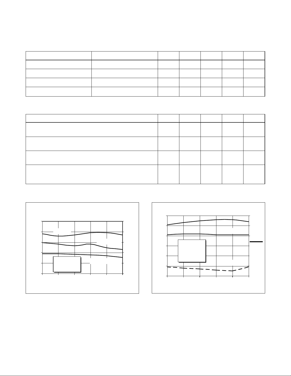
Maximum Ratings
Parameter Symbol Value Unit
Drain-Source Voltage V
Gate-Source Voltage V
Operating Junction T emperature T
T otal Device Dissipation at T
Above 25°C derate by 0.7 W/°C
Storage T emperature T
Thermal Resistance (T
flange
= 25°C P
flange
= 70°C) R
1
DSS
GS
J
D
STG
qJC
65 Vdc
±20 Vdc
200 °C
120 Watts
150 °C
1.4 °C/W
e
PTF 10045
y
y
s
e
Electrical Characteristics (100% T ested)
Characteristic Conditions Symbol Min T yp Max Units
Drain-Source Breakdown Voltage VGS = 0 V , ID = 25 mA V
(BR)DSS
Drain-Source Leakage Current VDS = 28 V , VGS = 0 V I
Gate Threshold Voltage VDS = 10 V , ID = 75 mA V
Forward Transconductance VDS = 10 V , ID = 3 A g
DSS
GS(th)
fs
65 — — Volts
— — 1.0 mA
3.0 — 5.0 Volts
— 2.0 — Siemens
RF Specifications (100% T ested)
Characteristic Symbol Min T yp Max Units
Common Source Power Gain
(V
Power Output at 1 dB Compression
(V
Drain Efficiency
(V
Load Mismatch Tolerance
(V
all phase angles at frequency of test)
= 28 V , P
DD
= 28 V , IDQ = 380 mA, f = 1650 MHz) P-1dB 30 35 — Watts
DD
= 28 V , P
DD
= 28 V , P
DD
= 30 W, IDQ = 380 mA, f = 1650 MHz) G
OUT
= 30 W, IDQ = 380 mA, f = 1650 MHz) h 40 43 — %
OUT
= 30 W, IDQ = 380 mA, f = 1650 MHz— Y — — 10:1 —
OUT
ps
10.0 11.5 — dB
Typical Performance
Typical P
13
12
11
Gain
10
9
8
1400 1450 1500 1550 1600 1650
, Gain & Efficiency
OUT
vs. Frequency
Gain (dB)
VDD = 28 V
= 380 mA
I
DQ
Outp ut P ower (W)
Frequency (MHz)
(at P-1dB)
Efficiency (%)
12
70
60
50
40
30
Output Power & Efficienc
20
11
10
9
Gain (dB)
8
7
6
1600 1610 1620 1630 1640 1650
Broadband Test Fixture Performance
Gain
Efficiency (%)
VDD = 28 V
= 380 mA
I
DQ
= 30 W
P
OUT
Frequency (MHz)
Return L oss (d B )
60
50
40
0
30
- 5
20
-10
10
-15
0
Efficienc
Return Los
2
 Loading...