

Ericsson PTF10043 Datasheet
PTF 10043
12 Watts, 1.9–2.0 GHz
GOLDMOS® Field Effect Transistor
Description
The PTF 10043 is an internally matched GOLDMOS FET intended
for large signal amplifier applications from 1.9 to 2.0 GHz. Rated at
12 watts, it operates at 45% efficiency with 12 dB gain. Nitride surface passivation and full gold metallization ensure excellent device
lifetime and reliability.
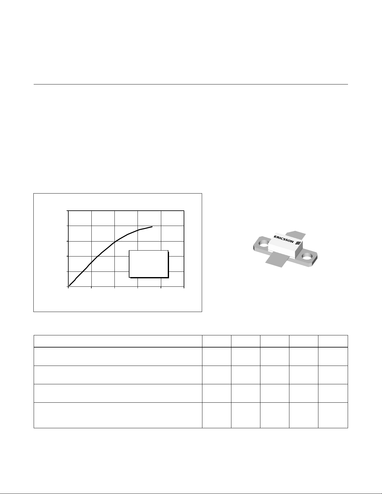
Typica l Output Power vs. Input Power
20
16
12
8
4
Output Power (Watts)
0
0.0 0.2 0.4 0.6 0.8 1.0
Input Power (Watts)
VDD = 26 V
I
= 150 mA
DQ
f = 2.0 GHz
INTERNALLY MATCHED
Performance at 2.0 GHz, 26 Volts
- Output Power = 12 Watts Min
- Power Gain = 12 dB Typ at 3 Watts
- Efficiency = 45% Typ
Full Gold Metallization
Silicon Nitride Passivated
Back Side Common Source
Excellent Thermal Stability
• 100% Lot Traceability
10043
A-1234569834
Package 20222
RF Specifications (100% Tested)
Characteristic Symbol Min Typ Max Units
Gain
(V
Power Output at 1 dB Compressed
(V
Drain Efficiency
(V
Load Mismatch Tolerance
(V
—all phase angles at frequency of test)
All published data at T
= 26 V , P
DD
= 26 V , P
DD
= 26 V , P
DD
= 26 V , P
DD
= 3 W, IDQ = 150 mA, f = 1.93, 2.0 GHz) G
OUT
= 12 W, IDQ = 150 mA, f = 2.0 GHz) p-1dB 12 1 4 — Watts
OUT
= 12 W, IDQ = 150 mA, f = 2.0 GHz) h
OUT
= 12 W, IDQ = 150 mA, f = 2.0 GHz Y — — 10:1 —
OUT
= 25°C unless otherwise indicated.
CASE
ps
D
11 12 — dB
40 45 — %
e
1
PTF 10043
e
Electrical Characteristics (100% Tested)
Characteristic Conditions Symbol Min Typ Max Units
Drain-Source Breakdown Voltage VGS = 0 V , ID = 5 mA V
Zero Gate Voltage Drain Current VDS = 26 V , VGS = 0 V I
Gate Threshold Voltage VDS = 10 V , ID = 75 mA V
Forward Transconductance VDS = 10 V , ID = 2 A g
(BR)DSS
DSS
GS(th)
fs
65 ——Volts
——1.0 mA
3.0 — 5.0 Volts
— 0.8 — Siemens
Maximum Ratings
Parameter Symbol Value Unit
Drain-Source Voltage V
Gate-Source Voltage V
Operating Junction Temperature T
Total Device Dissipation P
Above 25°C derate by 0.31 W/°C
Storage Temperature Range T
Thermal Resistance (T
= 70°C) R
CASE
DSS
GS
J
D
STG
qJC
65 Vdc
±20 Vdc
200 °C
55 Watts
–40 to +150 °C
3.2 °C/W
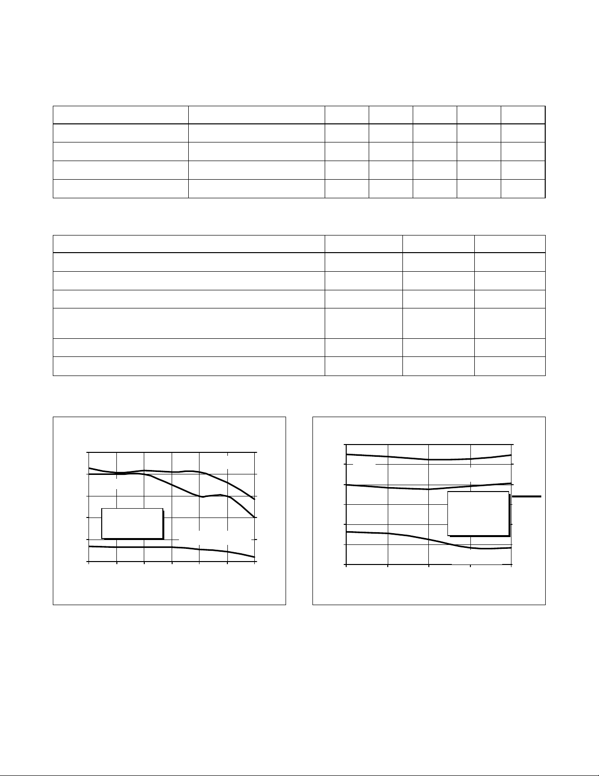
Typical Performance
P
, Gain & Efficiency
OUT
16
15
14
Gain
13
12
11
Gain
VDD = 26 V
I
= 150 mA
DQ
1750 1800 1850 1900 1950 2000 2050
(at P-1dB)
Output Power (W)
vs. Frequency
Eff iciency
F requency (MHz)
60
50
40
30
20
10
Output Power & Efficiency
Broadband Test Fix ture Pe rforma nce
14
12
Gain
10
8
Gain (dB)
6
4
2
1900 1925 1950 1975 2000
Frequency (MHz)
Efficiency (%)
VCC = 26 V
I
= 150 mA
DQ
P
= 10 W
OUT
R eturn Loss
60
50
40
- 5
30
20
-15
10
-25
0
-35
Efficiency (%)
Return Loss (dB)
2
 Loading...