

Page 1
查询PKF5510PI供应商
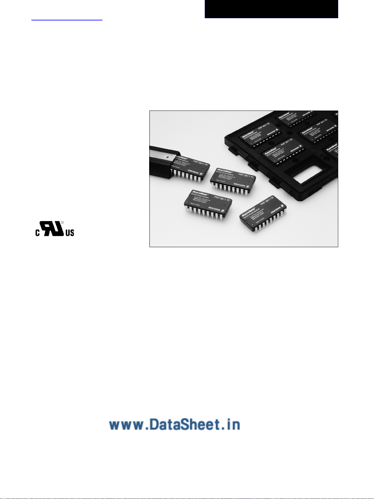
• SMD and through-hole versions with
ultra low component height 8 mm
(0.315 in.)
• 18–72 V input voltage range
• 82% efficiency (typ at 5 V)
• 1,500 Vdc isolation voltage
• Switching frequency syncronization
• MTBF >4.9 million hours at +55°C
case temperature (+40°C ambient)
• Low EMI measured according to
CISPR 22 and FCC part 15J
PKF 5000 I
5–6 W DC/DC Power Modules
Wide Input Series
Patents
US: D357901 DE: M94022763
The MacroDens™ PKF 5000 I series true component
level on-board DC/DC power modules are intended
as distributed power sources in decentralized 24, 48
and 60V DC power systems. Utilization of thick film
technology and a high degree of silicon integration
has made it possible to achieve a MTBF of more than
4.9 million hour.
The highly reliable and rugged over-moulded design
and the ultra low height of these DC/DC power
modules makes them particularly suited for Information Technology and Telecom (IT&T) and other
demanding industrial applications, with board
spacing down to 15 mm or 0.6 in. These DC/DC
power modules are optimized for free convection
cooling and have an operational ambient temperature
range in compliance with present and future
application needs, including non temperature controlled environments.
The mechanical design offers the choice of surface
mount or through-hole versions, delivered in readyto-use tubes, trays or tape & reel package, and
compatibility with semi and fully aqueous cleaning
processes.
The PKF series is manufactured using highly
automated manufacturing lines with a world-class
quality commitment and a five-year warranty.
Ericsson Microelectronics AB has been an ISO 9001
certified supplier since 1991. For a complete product
program please reference the back cover.
E
Page 2
General
Absolute Maximum Ratings
Characteristics Unit
T
T
V
V
W
V
V
Input
V
V
V
C
P
P
Case temperature at full output power –45
C
Storage temperature –55 +125 °C
S
Continuous input voltage
I
Isolation voltage
ISO
(input to output test voltage)
Transient input energy
tr
Remote control voltage pin 10,11
RC
Output adjust voltage pin 8, 9
adj
< T
T
C
unless otherwise specified
Cmax
Characteristics max Unit
Input voltage range
I
Turn-off input voltage
Ioff
Turn-on input voltage
Ion
Input capacitance
I
Input idling power
Ii
Input stand-by power
RC
1)
Conditions
1)
(See typical characteristics)
(See typical characteristics)
=0,TC= – 30…+90°C
I
O
= – 30…+90°C
T
C
RC connected to pin 17
min
max
+100 °C
–0.5 +75 Vdc
1,500
0.01
–5
–5
min
18
15
typ
17.4 V
+16 Vdc
+40 Vdc
72 V
16 V
17.9
1.4 mF
(V
= 27V)
I
(V
= 53V)
I
(V
= 27V)
I
(V
= 53V)
I
244
240
18
67
Vdc
Ws
mW
mW
Stress in excess of Absolute Maximum Ratings may cause permanent damage. Absolute
Maximum Ratings, sometimes referred to as
no destruction limits, are normally tested
with one parameter at a time exceeding the
limits of Output data or Electrical Characteristics. If exposed to stress above these
limits, function and performance may degrade in an unspecified manner.
NOTES:
1)
The input voltage range 18…72 Vdc meets
the European Telecom Standard
ETS 300 132-2 Nominal input voltage range
in 48 V and 60 V dc power systems, – 40.5…
–57.0 V and –50.0… – 72.0 V respectively. At
input voltages exceeding 72 V (abnormal
voltage) the power loss will be higher than at
normal input voltage and T
max +90°C. Absolute max continuous input
voltage is 75 Vdc. Output characteristics will
be marginally affected at input voltages
exceeding 72 V.
2)
The test is applicable for through-hole
versions.
must be limited to
C
Environmental Characteristics
Characteristics
Vibration
(Sinusoidal)
Random
vibration
Shock
(Half sinus)
Temperature
change
Accelerated
damp heat
Solder
resistability
Aggressive
environment
2)
JESD 22-B103
(IEC 68-2-6 Fc)
MIL-STD-883
Method 2026
(IEC 68-2-34 Ed)
JESD 22-B104
(IEC 68-2-27 Ea)
JESD 22-A104
(IEC 68-2-14 Na)
JESD 22-A101
(IEC 68-2-3 C
with bias)
a
JESD 22-B106
(IEC 68-2-20 Tb 1A)
IEC 68-2-11 K
a
2 EN/LZT 146 32 R1A (Replaces EN/LZT 137 27 R3) ©Ericsson Microelectronics, June 2000
Test procedure & conditions
Frequency 10…500 Hz
Amplitude 0.75 mm
Acceleration 10 g
Number of cycles 10 in each axis
Frequency 10…500 Hz
Acceleration density
spectrum 0.5 g
2
/Hz
Duration 10 min in 3 directions
Reproducability medium (IEC 62-2-36)
Peak acceleration 200 g
Shock duration 3 ms
Temperature –40°C…+125°C
Number of cycles 500
Temperature 85°C
Humidity 85% RH
Duration 1000 hours
Temperature, solder 260°C
Duration 10…13 s
Duration 96 h
Temperature 35°C
Concentration 5 %
Page 3
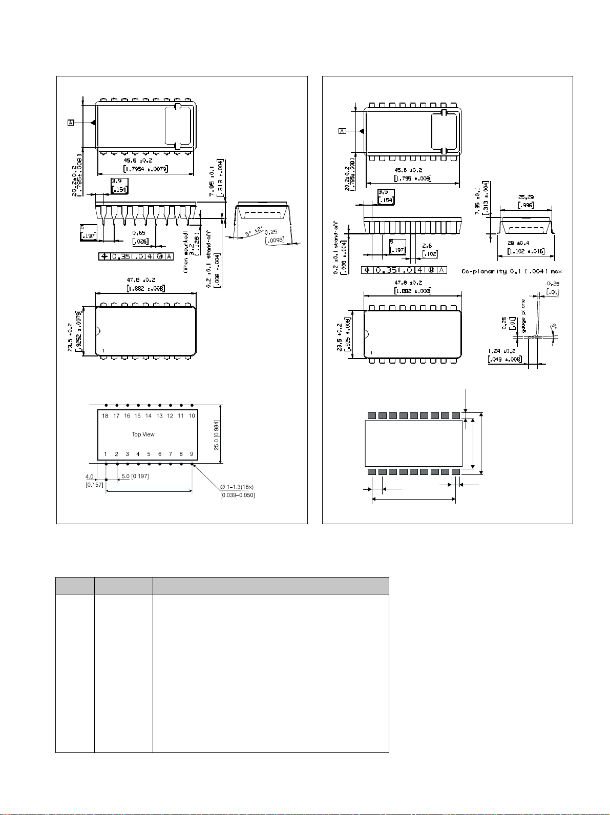
Mechanical Data
Through-hole version
Surface-mount version
Foot print Component side
40.0 [1.575]
Dimensions in mm (in)
Foot print Component side
Connections
Pin Designation Function
1 Out 1 Output 1. Positive voltage ref. to Rtn.
2 Rtn Output return.
3–6 NC Not connected.
7 Sync Synchronization input.
8V
9 NOR Connection of Nominal Output voltage Resistor. (See output
10 Aux Internally connected to pin 11.
11 RC Remote control and turn-on/off input voltage adjust. Used to turn-on
12–16 NC Not connected.
17 –In Negative input.
18 +In Positive input.
adj
Output voltage adjust. To set typical output voltage (VOi)
connect pin 8 to pin 9.
voltage adjust p. 12).
and turn-off output.
16
18
17
12 345 6789
5.0 [0.197]
131415
40.0 [1.575]
12
Weight
Maximum 20 g (0.71 oz).
Case
The case consists of semiconductor grade
epoxy with embedded pins.
Coefficient of thermal expansion (CTE) is
typ. 15 ppm/°C.
Connection Pins
Base material is copper (Cu), first plating is
nickel (Ni) and second (outer) plating is
palladium (Pd).
1011
2.8 [0.110]
29.6 [1.165]
24.0 [0.945]
3.6 [0.142]
Dimensions in mm (in)
EN/LZT 146 32 R1A (Replaces EN/LZT 137 27 R3) ©Ericsson Microelectronics, June 2000
3
Page 4
Thermal Data
Over-temperature protection
The PKF 5000 series will automatically shut down when the internal
junction temperature of the control IC in the converter reaches typ.
150 °C.
It will automatically re-start when the junction temperature cools
below typ. 140°C.
Two-parameter model
This model provides a more precise description of the thermal characteristics to be used for thermal calculations.
Thermally the power module can be considered as a component and
the case temperature can be used to characterize the properties. The
thermal data for a power module with the substrate in contact with
the case can be described with two thermal resistances. One from the
case to ambient air and one from case to PB (Printed Board).
The thermal characteristics can be calculated from the following
formula:
= (TC–TA)×(R
T
PB
th C–PB+Rth C–A
Where:
Pd: dissipated power, calculated as PO ×(l/h–1)
: max average case temperature
T
C
: ambient air temperature at the lower side of the power
T
A
module
: temperature in the PB between the PKF connection pins
T
PB
: thermal resistance from case to PB under the power
R
th C-PB
module
: thermal resistance from case to ambient air
R
th C-A
v: velocity of ambient air.
R
is constant and Rth
th C-PB
Free convection is equal to an air velocity of approx. 0.2 – 0.3 m/s.
See figure below.
)/R
th C–A–Pd×Rth C–PB+TA
is dependent on the air velocity.
C-A
Reflow Soldering Information
The PKF series of DC/DC power modules are manufactured in surface
mount technology. Extra precautions must therefore be taken when
reflow soldering the surface mount version. Neglecting the soldering
information given below may result in permanent damage or significant degradation of power module performance.
The PKF series can be reflow soldered using IR, Natural Convection,
Forced Convection or Combined IR/Convection Technologies. The high
thermal mass of the component and its effect on DT (°C) requires that
particular attention be paid to other temperature sensitive components.
IR Reflow technology may require the overall profile time to be extended to approximately 8–10 minutes to ensure an acceptable DT.
Higher activity flux may be more suitable to overcome the increase in
oxidation and to avoid flux burn-up.
The general profile parameters detailed in the diagram, with this extended time to reach peak temperatures, would then be suitable.
Note! These are maximum parameters. Depending on process variations, an appropriate margin must be added.
Palladium plating is used on the terminal pins. A pin temperature (T
in excess of the solder fusing temperature (+183°C for Sn/Pb 63/37)
for more than 25 seconds and a peak temperature above 195°C, is
required to guarantee a reliable solder joint.
Both pin 1 and pin 9 must be monitored.
No responsibility is assumed if these recommendations are not
strictly followed.
4 EN/LZT 146 32 R1A (Replaces EN/LZT 137 27 R3) ©Ericsson Microelectronics, June 2000
)
p
Page 5
Safety
Electrical Data
The PKF Series DC/DC power modules are designed in accordance
with EN 60 950, Safety of information technology equipment including
electrical business equipment. SEMKO approval pending.
The DC/DC power module shall be installed in an end-use equipment and considerations should be given to measuring the case temperature to comply with T
nent tests are conducted with the input protected by an external 3 A
fuse. The need for repeating these tests in the end-use appliance shall
be considered if installed in a circuit having higher rated devices.
When the supply to the DC/DC power module meets all the requirements for SELV (<60 V dc), the output is considered to remain within
SELV limits (level 3). The isolation is an operational insulation in
accordance with EN 60 950.
The DC/DC power module is intended to be supplied by isolated
secondary circuitry and shall be installed in compliance with the
requirements of the ultimate application. If they are connected to a
60 V DC system reinforced insulation must be provided in the power
supply that isolates the input from the mains. Single fault testing in
the power supply must be performed in combination with the
DC/DC power module to demonstrate that the output meets the
requirement for SELV. One pole of the input and one pole of the
output is to be grounded or both are to be kept floating.
The terminal pins are only intended for connection to mating connectors of internal wiring inside the end-use equipment.
These DC/DC power modules may be used in telephone equipment
in accordance with paragraph 34 A.1 of UL 1459 (Standard for Telephone Equipment, second edition).
The galvanic isolation is verified in an electric strength test. Test
voltage (V
production the test duration is decreased to 1 s.
The capacitor between input and output has a value of 1 nF and the
leakage current is less than 1µA @ 53 Vdc.
The case is designed in non-conductive epoxy. Its flammability
rating meets UL 94V-0. The oxygen index is 34%
) between input and output is 1,500 V dc for 60 s. In
ISO
max
when in operation. Abnormal compo-
C
.
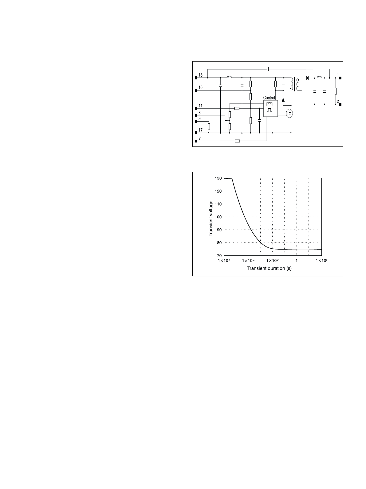
Fundamental circuit diagrams
Single output
Transient input voltage
Single voltage pulse at +25 °C ambient temperature.
EN/LZT 146 32 R1A (Replaces EN/LZT 137 27 R3) ©Ericsson Microelectronics, June 2000
5
Page 6

PKF 5510 PI, SI
TC = –30…+90°C, VI = 18 ...72V and pin 8 connected to pin 9 unless otherwise specified.
Output
Characteristics Conditions
V
Oi
V
O
t
tr
V
tr
T
coeff
t
r
Output voltage initial
setting and accuracy
Output adjust range
1)
Output voltage
tolerance band
Idling voltage
Line regulation
Load regulation
Load transient
recovery time
Load transient voltage
Temperature coefficient
Ramp-up time
TC = +25°C, IO = 1.5 A, VI = 53 V
Long term
drift incl.
= 0 A
I
O
= 1,5 A
I
O
= 0.15…1.5 A, VI = 53 V
I
O
= 0.15…1.5 A, VI = 53 V
I
O
load step = 0.75 A
2)
IO =1.5 A, TC =+40…+90ºC
I
1.5 A, 0.15…1.5 ×V
O =
min
3.27 3.30 3.33 V
2.80 3.80 V
IO = 0.15…1.5 A
IO = 0.15…1.5 A, VI = 19–72V
IO = 0.2…1.5 A, VI = 20-72V
3.00 3.46
3.13 3.46
3.17 3.42
VI = 18…36 V
VI = 38…60 V
= 50…72 V 15
V
I
50 200 mV
O
Output 1
typ
max
Unit
V
3.8 4.3 V
30
30 mV
100 ms
+150 mV
–150 mV
–0.4 mV/°C
2ms
s
I
O
P
Omax
I
lim
I
sc
V
Oac
SVR
1)
See also Operating Information.
2)
See Typical Characteristics.
Start-up timet
Output current
Max output power
Current limiting
threshold
Short circuit current
Supply voltage rejection (ac)
O
From V
connection to VO = 0…0.9×V
I
Oi
0 1.5 A
2)
Calculated value
TC <T
, VO = 3.0 V
Cmax
5W
1.65 2.30 2.50 A
VO = 0.2…0.5 V, TA =+25°C
20 Hz…5 MHz
IO = 1.5 AOutput ripple & noise
0.6 …50 MHz
f = 100 Hz sine wave, 1V
(SVR = 20 log (1 V
p-p/VOp-p
, VI = 53 V
p-p
))
5ms
2.7 A
20 70 mV
80 dBmV
45 dB
= 0.15…1.5A, VI = 53 V
I
Miscellaneous
Characteristics Conditions Unit
VI = 27 V
h
P
d
Efficiency
Power dissipation
IO = 1.5 A
= 53 V 75 78
V
I
VI = 27 V
= 53 V
V
I
min
78 80
typ
max
1.2 1.4
1.4 1.7
p-p
%
W
6 EN/LZT 146 32 R1A (Replaces EN/LZT 137 27 R3) ©Ericsson Microelectronics, June 2000
Page 7

PKF 5611 PI, SI
TC = –30…+90°C, VI = 18 ...72V and pin 8 connected to pin 9 unless otherwise specified.
Output
Characteristics Conditions
V
V
t
tr
V
T
t
r
t
s
I
O
P
I
lim
I
sc
V
SVR
1)
See also Operating Information.
2)
See Typical Characteristics.
Output voltage initial
Oi
setting and accuracy
Output adjust range
Output voltage
O
tolerance band
Idling voltage
Line regulation
Load regulation
Load transient
recovery time
Load transient voltage
tr
Temperature coefficient
coeff
Ramp-up time
Start-up time
Output current
Max output power
Omax
Current limiting
threshold
Short circuit current
Oac
Supply voltage rejection (ac)
1)
Long term drift
included
TC = +25°C, IO = 0.2 A, VI = 53 V
= 0 A
I
O
= 1.2 A
I
O
= 0.3…1.2 A, VI = 27 V
I
O
= 0.12…12 A, VI = 53 V
I
O
load step = 0.6 A
2)
IO = 1.2 A, TC =+40…+ 90ºC
IO = 1.2 A, 0.1…0.9 ×V
= 0.1…1.2 A, VI = 53 V
I
O
From V
2)
Calculated value
TC <T
Cmax
VO = 0.2…0.5 V, TA =+25°C
I
= 1.2 AOutput ripple & noise
O
f = 100 Hz sine wave, 1V
(SVR = 20 log (1 V
IO = 0.15…1.2 A
VI = 18…36 V
= 38…60 V
V
I
VI = 50…72 V 10
O
connection to VO = 0…0.9 ×V
I
, VO = 4.0 V
20 Hz…5 MHz
0.6 …50 MHz
, VI = 53 V
p-p
))
p-p/VOp-p
min
Output 1
typ
max
Unit
5.02 5.05 5.08 V
4.30 5.80 V
4.85 5.25 V
5.7 6.0 V
50
20 mV
135 mV
330 ms
+120 mV
–120 mV
–1.1 mV/°C
125ms
Oi
4.8 10 ms
01.2A
6W
1.3 1.8 2.0 A
2.0 3.5 A
50 150 mV
p-p
80 dBmV
60 dB
Miscellaneous
Characteristics Conditions Unit
VI = 27 V
h
P
EN/LZT 146 32 R1A (Replaces EN/LZT 137 27 R3) ©Ericsson Microelectronics, June 2000
d
Efficiency
Power dissipation
IO = 1.2 A
V
= 53 V
I
VI = 27 V
= 53 V
V
I
min
79 83
79 81
typ
max
1.2 1.6
1.4 1.6
%
W
7
Page 8

PKF 5617 PI, SI
TC = –30…+90°C, VI = 18 ...72V and pin 8 connected to pin 9 unless otherwise specified.
Output
Characteristics Conditions
V
V
t
V
T
t
t
I
P
I
I
V
Oi
O
tr
tr
coeff
r
s
O
Omax
lim
sc
Oac
Output voltage initial
setting and accuracy
Output adjust range
1)
Output voltage
tolerance band
Idling voltage
Line regulation
Load regulation
Load transient
recovery time
Load transient voltage
Temperature coefficient
Ramp-up time
Start-up time
Output current
Max output power
2)
Current limiting
threshold
Short circuit current
Output ripple & noise
TC = +25°C, IO = 0.72 A, VI = 53 V
Long term drift
included
I
= 0 A, VI =53 V
O
I
=0.86 A
O
I
= 0.08…0.86 A, VI = 27 V
O
I
= 0.086…0.86 A, VI = 53 V
O
load step = 0.43 A
2)
IO = 0.86 A, TC =+40…+90ºC
IO = I
Omax,
I
= 0.086…0.86 A, VI = 53 V
O
From V
connection to VO = 0.9×V
I
Calculated value
TC <T
Cmax
VO = 0.2…0.5 V, TA =+25°C
I
=0.86 A
O
0.1…0.9 ×V
, VO = 4.0 V
Output 1
min
typ
6.95 7.00 7.05 V
5.95 8.05 V
IO = 0.086…0.86 A
6.65 7.35 V
7.5 7.9 V
VI = 18…36 V
VI = 38…60V
10
10 mV
VI = 50…72 V 10
120 mV
350 ms
+130 mV
–130 mV
–1.2 mV/°C
O, VI
= 53 V
Oi
135ms
0 0.86 A
6W
1.0 1.2 1.6 A
1.8 3.5 A
20 Hz…5 MHz
50 150 mV
0.6 …50 MHz
max
Unit
510ms
p-p
80 dBmV
SVR
*1)
12)
Supply voltage rejection (ac)
See also Operating Information.
See Typical Characteristics.
f = 100 Hz sine wave, 1V
(SVR = 20 log (1 V
p-p/VOp-p
, VI = 53 V
p-p
))
60 dB
Miscellaneous
Characteristics Conditions Unit
VI = 27 V
h
P
d
Efficiency
Power dissipation
IO = 0.86 A
= 53 V
V
I
VI = 27 V
= 53 V
V
I
min
80 84
80 82
8 EN/LZT 146 32 R1A (Replaces EN/LZT 137 27 R3) ©Ericsson Microelectronics, June 2000
typ
max
1.1 1.5
1.3 1.5
%
W
Page 9

Typical Characteristics
PKF 5510 PI, SI
Output characteristic (typ)
Temperature coefficient
Power derating
Turn-on/turn/off input voltage
Efficiency (typ)
@ TA = +25°C
Dynamic load response (typ)@+25C
The output voltage
deviation is determined by the load
transient (dI/dt)
100 mV/div
1 A/div
0.2 ms/div
Load change:
dI/dt» 4 A/ms
Output characteristic (typ)
Temperature coefficient
PKF 5611 PI, SI
Power derating
Turn-on/turn/off input voltage
Efficiency (typ)
@ TA = + 25°C
Dynamic load response (typ)@+ 25C
The output voltage
deviation is determined by the load
100 mV/div
1 A/div
0.2 ms/div
transient (dI/dt)
Load change:
dI/dt» 4 A/ms
EN/LZT 146 32 R1A (Replaces EN/LZT 137 27 R3) ©Ericsson Microelectronics, June 2000
9
Page 10

PKF 5617 PI, SI
Output characteristic (typ)
Temperature coefficient
Power derating
Turn-on/turn/off input voltage
Efficiency (typ) @ TA = +25°C
Dynamic load response (typ)@+25C
The output voltage
deviation is determined by the load
100 mV/div
1 A/div
0.2 ms/div
transient (dI/dt)
Load change:
dI/dt» 4 A/ms
10 EN/LZT 146 32 R1A (Replaces EN/LZT 137 27 R3) ©Ericsson Microelectronics, June 2000
Page 11

EMC Specifications
The fundamental switching frequency is 510 kHz ± 26 kHz.
Conducted EMI (input teminals)
PKF series typical conducted EMI performance
Test set up
EFT
Electrical Fast Transients on the input terminals could affect the
output voltage regulation causing functional errors on the Printed
Board Assembly (PBA). The PKF power modules withstand EFT
levels of 0.5 kV keeping V
within the tolerance band and
O
2.0 kV without destruction. Tested according to IEC publ. 801-4.
Output Ripple & Noise (VOac)
Output ripple is measured as the peak to peak voltage of the fundamental switching frequency.
Operating Information
Fuse Considerations
To prevent excessive current from flowing through the input supply
line, in the case of a short-circuit across the converter input, an
external fuse should be installed in the non-earthed input supply
line. We recommend using a fuse rated at approximately 2 to 4 times
the value calculated in the formula below:
P
max
I
=
max
in
For further information, please refer to the fuse manufacturer .
O
(h
× V
)
min
min
I
The PKF meets class A in VDE 0871/0878, FCC Part 15J, and CISPR 22
(EN 55022), except for the fundamental switching frequency.
Conducted EMS
Electro Magnetic Susceptibility is measured by injection of electrical disturbances on the input terminals. No deviation outside
tolerance band will occur under the following conditions:
the V
O
Frequency range Voltage level
0.15...300 MHz 1.0 V
rms
The signal is amplitude modulated with 1 kHz/80% and applied
both differential and common mode.
Radiated EMS (Electro-Magnetic Fields)
Radiated EMS is measured according to test methods in
IEC Standard publ. 801-3. No deviation outside the VO tolerance
band will occur under the following conditions:
Frequency range Voltage level
rms
rms
rms
/m
/m
/m
0.01...200 MHz 3 V
200...1,000 MHz 3 V
1...12 GHz 10 V
ESD
Electro Static Discharge is tested according to IEC publ. 801-2. No
destruction will occur if the following voltage levels are applied to
any of the terminal pins:
Test Voltage level
Air discharge ±4 kV
Contact discharge ±2 kV
Remote Control (RC)
Turn-on or turn-off can be realized by using the RC-pin. If pin 11 is
connected to pin 17 the power module turns off. Normal operation is
achieved if pin 11 is open (NC) . To ensure safe turn-off the voltage
difference between pin 11 and 17 shall be less than 2.0V. RC is an
TTL open collector compatible output with a sink capacity >300 mA
(see fig. 1).
Figure 1
Over Voltage Protection (OVP)
The remote control can also be utilized for OVP by using the external circuitry in figure 2. Resistor values are for 5V output applications, but can easily be adjusted for other output voltages and the
desired OVP level.
EN/LZT 146 32 R1A (Replaces EN/LZT 137 27 R3) ©Ericsson Microelectronics, June 2000
11
Page 12

Figure 2
Output Voltage Adjust (V
adj
)
Output voltage, VO, can be adjusted by using an external resistor.
Typical adjust range is ± 15%. If pin 8 and 9 are not connected together the output will decrease to a low value.To increase V
a resis-
O
tor should be connected between pin 8/9 and 17, and to decrease V
resistor should be connected between pin 8 and 9 (see fig. 4).
Typical required resistor value to increase V
R
= k1×(k2 – VO)/(VO – VOi), (kW)
adj
where V
is the desired output voltage
O
is given by:
O
VOi is the typical output voltage initial setting
and k
=3.18 k2=3.86 PKF 5510
1
k1=3.18 k2=5.93 PKF 5611
=3.18 k2=8.05 PKF 5617
k
1
Typical required resistor value to decrease V
R
= k3 × (VOi –VO)/(VO – k4), (kW)
adj
where k
=13.0 k4=2.75 PKF 5510
3
is given by:
O
k3=12.6 k4=4.28 PKF 5611
=12.6 k4=5.95 PKF 5617
k
3
Capacitive Load
The PKF series has no maximum limit for capacitive load on the output. The power module may operate in current limiting mode during
start-up, affecting the ramp-up and the start-up time. For optimum
start performance we recommend maximum 100 mF/A of I
capacitors at the point of load for best performance.
Parallel Operation
Paralleling of several converters is easily accomplished by direct
a
O
connection of the output voltage terminal pins. The load regulation
characteristic is specifically designed for optimal paralleling performance. Load sharing between converters will be within ±10%. It
is recommended not to exceed P
= n × 0.9 × P
O
max
O
, where P
the maximum converter output power and n the number of paralleled
converters, to prevent overloading any of the converters and thereby
decreasing the reliability performance.
Current Limiting Protection (I
lim
)
The output power is limited at loads above the output current
limiting threshold (I
), specified as a minimum value.
lim
Synchronization (Sync)
It is possible to synchronize the switching frequency to an external
symmetrical clock signal. The input is TTL-compatible and referenced to the input pin 17.
Figure 4
. Connect
O
max
O
is
Characteristic min typ max unit
High level 2.2 6.5 V
Threshold level
Low level 0 0.4 V
Sink current 1.5 mA
Sync. frequency 520 688 kHz
*)
Rise time <10ns
*)
1.2 1.7 2.2 V
Input and Output Impedance
Figure 3
Voltage Margining
For voltage controlled margining e.g. at final test, the following
setup can be used. By increasing the control voltage V1 to +10V the
output voltage decreases 5% of V
, and by decreasing V1 to –10V
Oi
the output voltage increases 5%.
12 EN/LZT 146 32 R1A (Replaces EN/LZT 137 27 R3) ©Ericsson Microelectronics, June 2000
Both the source impedance of the power feeding and the load impedance will interact with the impedance of the DC/DC power module.
It is most important to have the ratio between L and C as low as
possible, i.e. a low characteristic impedance, both at the input and
output, as the power modules have a low energy storage capability.
Use an electrolytic capacitor across the input if the source is larger
than 10 mH. Their equivalent series resistance together with the
capacitance acts as a lossless damping filter. Suitable capacitor values
are in the range 10–100 mF.
Page 13

Delivery Package Information
Tubes
The PKF-series is delivered in tubes (designated by /A) with a length
of 500 mm (19.69 in), see fig. 5.
Figure 5
Specification
Material: Antistatic coated PVC
Max surface resistance: 10
Color: Transparent
Capacity: 10 power modules/tube
Weight: Typ. 60 g
End stops: Pins
11
W/
Capacity: 15 power modules/tray
Stacking pitch: 10.16 mm
Weight: Typ. 130 g
Min. order quantity: 150 pcs (one box contains 10 full trays)
Tape & Reel
SMD versions, SI, can be delivered in standard tape & reel package
(designated by /C) on request, see fig. 7. For more information, please
contact your local Ericsson sales office.
Trays
SMD versions, SI, can be delivered in standard JEDEC trays
(designated by /B) on request, see fig. 6. For more information,
please contact your local Ericsson sales office.
Figure 6
Figure 7
Specification
Tape material: Conductive polystyrene (PS)
Tape width: 72 mm
Tape pitch: 36 mm
5
Max surface resistance: 10
W/
Tape color: Black
Cover tape color: Transparent
Reel diameter: 13"
Reel hub diameter: 7"
Reel capacity: 150 pcs
Full reel weight: Typ. 3.7 kg
Min. order quantity: 300 pcs (one box contains two reels)
Specification
Material: Polypropylene (PP)
Max temperature: 125 ºC
5
Max surface resistance: 10
W/
Color: Black
EN/LZT 146 32 R1A (Replaces EN/LZT 137 27 R3) ©Ericsson Microelectronics, June 2000
13
Page 14

Quality
Reliability
Meantime between failure (MTBF) is calculated to >4.9 million
hours at full output power and a pin temperature of +55°C
= +40°C), using the Ericsson failure rate data system. The
(T
A
Ericsson failure rate data system is based on field failure rates and is
continously updated. The data corresponds to actual failure rates of
components used in Information Technology and Telecom equipment
in temperature controlled environments (T
is considered to have a confidence level of 90%. For more information
see Design Note 002.
Quality Statement
The products are designed and manufactured in an industrial environment where quality systems and methods like ISO 9000, 6s and
SPC, are intensively in use to boost the continuous improvements
strategy. Infant mortality or early failures in the products are screened
out by a burn-in procedure and an ATE-based final test.
Conservative design rules, design reviews and product qualifications,
plus the high competence of an engaged work force, contribute to the
high quality of our products.
Warranty
Ericsson Microelectronics warrants to the original purchaser or end
user that the products conform to this Data Sheet and are free from
material and workmanship defects for a period of five (5) years from
the date of manufacture, if the product is used within specified conditions and not opened. In case the product is discontinued, claims
will be accepted up to three (3) years from the date of the discontinuation.
For additional details on this limited warranty please refer to Ericsson
Microelectronics AB’s “General Terms and Conditions of Sales”, or
individual contract documents.
= –5… +65°C). The data
A
Limitation of liability
Ericsson Microelectronics does not make any other warranties, expressed or implied including any warranty of merchantability or
fitness for a particular purpose (including, but not limited to, use in
life support applications, where malfunctions of product can cause
injury to a person’s health or life).
Information given in this data sheet is believed to be accurate and reliable. No responsibility is assumed for the consequences of its use nor for any infringement
of patents or other rights of third parties which may result from its use.
No license is granted by implication or otherwise under any patent or patent rights of
Ericsson Microelectronics. These products are sold only according to Ericsson Microelectronics’ general conditions of sale, unless otherwise confirmed in writing.
Specifications subject to change without notice.
14 EN/LZT 146 32 R1A (Replaces EN/LZT 137 27 R3) ©Ericsson Microelectronics, June 2000
Page 15

EN/LZT 146 32 R1A (Replaces EN/LZT 137 27 R3) ©Ericsson Microelectronics, June 2000
15
Page 16

Product Program
V
I
24/48/60 V
(max 75 Vdc)
VO/IO max
Output 1
3.3 V/1.5 A
5 V/1.2 A
7 V/0.86 A
P
max
O
5 W
6 W
6 W
Through-hole
PKF 5510 PI
PKF 5611 PI
PKF 5617 PI
*)
Ordering No.
See also Delivery Package Information
*)
SMD
PKF 5510 SI
PKF 5611 SI
PKF 5617 SI
Ericsson Microelectronics AB
SE-164 81 KISTA, Sweden
Phone: +46 8 757 5000
www.ericsson.com/microelectronics
For local sales contacts, please refer to our website
or call: Int. +46 8 757 4700, Fax: +46 8 757 4776
The latest and most complete infor-
mation can be found on our website!
Data Sheet
EN/LZT 146 32 R1A (Replaces EN/LZT 137 30 R5)
© Ericsson Microelectronics AB, June 2000
 Loading...