

Ericsson PBD3517-1NS, PBD3517-1SOS, PBD3517-1SOT Datasheet
PBD 3517/1
Stepper Motor
Drive Circuit
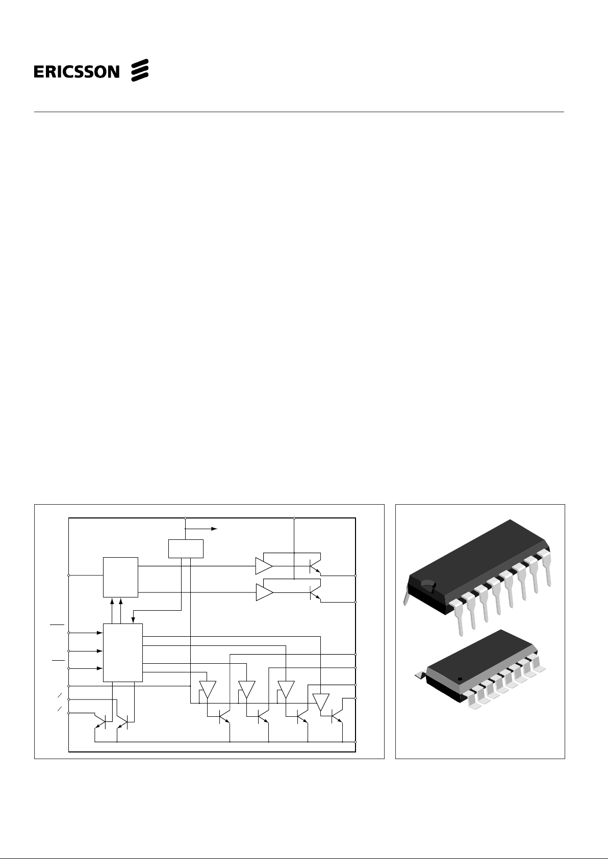
Figure 1. Block diagram.
February 1999
16-pin plastic DIP
16-pin SO (wide body)
RC
STEP
DIR
HSM
INH
O
A
OB
L
A
L
B
P
B2
P
B1
P
A2
P
A1
GND
V
CC
V
SS
PBD 3517/1
PQR
Mono
F - F
Phase
Logic
P
A
P
B
Description
PBD 3517/1 is a bipolar, monolithic, integrated circuit, intended to drive a stepper motor
in a unipolar, bilevel way.
One PBD 3517/1 and a minimum of external components form a complete control
and drive unit for LS-TTL- or microprocessor-controlled stepper motor system for
currents up to 500mA. The driver is suited for applications requiring least-posssible RFI.
Motor performance can be increased by operating in a bilevel drive mode. This
means that a high voltage pulse is applied to the motor winding at the beginning of a
step, in order to give a rapid rise of current.
Key Features
• Complete driver and phase logic on
chip
• 2 x 350 mA continuous-output current
• Half- and full-step mode generation
• LS-TTL-compatible inputs
• Bilevel drive mode for high step rates
• Voltage-doubling drive possibilities
• Half-step position-indication output
• Minimal RFI
• 16-pin plastic DIP package or 16 pin
small outline wide body
PBD 3517/1
PBD 3517/1
1
PBD 3517/1
2
Maximum Ratings
Parameter Pin No. Symbol Min Max Unit
Voltage
Logic supply 16 V
CC
07V
Second supply 15 V
SS
045V
Logic input 6, 7, 10, 11 VI -0.3 6 V
Current
Phase output 1, 2, 4, 5 I
P
0 500 mA
Second-level output 13, 14 I
L
-500 0 mA
Logic input 6, 7, 10, 11 I
I
-10 mA
The zero output 8, 9 I
Ο
6mA
Temperature
Operating junction temperature T
J
-40 +150 °C
Storage temperature T
S
-55 +150 °C
Power Dissipation (Package Data)
Power dissipation at TA = 25°C, DIP package. Note 2. P
D
1.6 W
Power dissipation, SO package. Note 3. P
D
1.3 W
Recommended Operating Conditions
Parameter Symbol Min Typ Max Unit
Logic supply voltage V
CC
4.75 5 5.25 V
Second-level supply voltage V
SS
10 40 V
Phase output current I
P
0 350 mA
Second-level output current I
L
-350 0 mA
Operating junction temperature T
J
-20 +125 °C
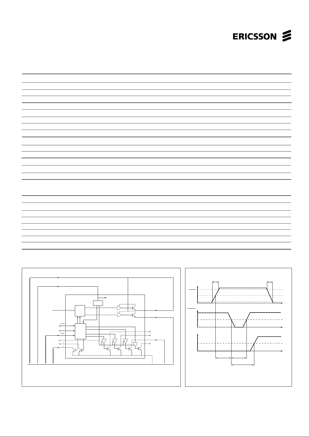
Set-up time t
s
400 ns
Step-pulse duration t
p
800 ns
Figure 2. Definition of symbols.
HSM
or
DIR
V
I
STEP
I
P
t
t
t
t
r
t
f
t
s
t
p
t
d
Figure 3. Timing diagram
.
RC 12
STEP 7
DIR 6
HSM 10
INH 11
O
A
9
OB 8
13 L
A
14 L
B
1 P
B2
2 P
B1
5 P
A2
4 P
A1
3 GND
V
CC
16
V
SS
15
PBD 3517/1
PQR
Mono
F - F
Phase
Logic
P
A
P
B
V
CC
V
SS
V
I
V
IH
V
IL
V
OCE Sat
V
LCE Sat
V
L
V
PCE Sat
V
P
IPI
PL
I
LL
I
L
IIIILI
IH
I
SS
I
CC
PBD 3517/1
3
Electrical Characteristics
Electrical characteristics at TA = +25°C, VCC = +5.0 V, VMM = +40 V, VSS = +40 V unless otherwise specified.
Ref.
Parameter Symbol Fig. Conditions Min Typ Max Unit
Supply current I
CC
2 INH = LOW 45 60 mA
2 INH = HIGH 12 mA
Phase outputs
Saturation voltage V
PCE Sat
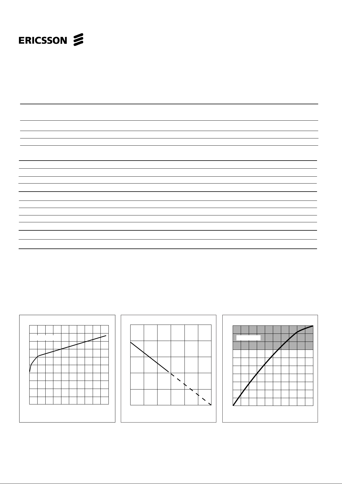
4IP = 350 mA 0.85 V
Leakage current I
PL
2VP = 0 V 500 µA
Turn on, turn off t
d
3 +70°C3µs
t
d
3 +125°C6µs
Second-level outputs
Saturation voltage V
LCE Sat
4IL = -350 mA 2.0 V
Leakage current I
LL
2VL = 0 V -500 µA
On time t
On
11 (note 4) 220 260 300 µs
Logic inputs
Voltage level, HIGH V
IH
2 2.0 V
Voltage level, LOW V
IL
2 0.8 V
Input current, low I
IL
2VI = 0.4 V -400 µA
Input current, high I
IH
2VI = 2.4 V 20 µA
Logic outputs
Saturation voltage V
ØCE Sat
5IØ = 1.6 mA 0.4 V
Notes
1. All voltages are with respect to ground. Current are positive into, negative out of specified terminal.
2 Derates at 12,8 mW/°C above +25°C.
3. Derates at 10.4 mW/°C above +25°C.
4. R
T
= 47 kΩ, CT = 10 nF.
Figure 5. Typical second level saturation
voltage vs output current.
Figure 4. Typical phase output saturation
voltage vs. output current.
Figure
2.5
2.0
1.5
1.0
0,5
0
0 0.1 0.2 0.50.40.3
V
LCE
sat [V]
I
L
[A]
TA= +25° C
2.5
2.0
1.5
1.0
0,5
0
0 50 100 150
Allowable power dissipation [W]
Ambient temrature [°C]
0.5
0.4
0.3
0.2
0.1
0
0 0.2 0.4 1.00.80.6
Output Current [A]
Output Voltage [V]
TA= +25° C
 Loading...