

Ericsson MGM 450, Monogram MGM 450 Maintenance Manual
LBI-38865A
Maintenance Manual
Monogram
UHF MOBILE RADIO
MODEL MGM 450
Series
ericssonz

LBI-38865
NOTICE!
This manual covers Ericsson and General Electric products manufactured and sold by Ericsson Inc.
NOTE
Repairs to this equipment should be m ade only by an authorized service technician or facility designated by the supplier.
Any repairs, alterations or substitution of recommended parts made by the user to th is equipment not approved by the
manufacturer could void the user’s authority to operate the equipment in addition to the manufacturer’s warranty.
NOTICE!
The software co nta ine d in this devi c e is co py right e d by E ric sson Inc . Unpu bli she d right s a re re ser ve d und er the copy rig ht
laws of the United States.
This manual is published by Ericsson Inc., without any warranty. Improvements and changes to this manual necessitated
by typographical e rror s, inacc uraci es of cu rr en t infor ma tion, o r im prov em en ts to prog ra ms and/or equ ipm ent, ma y be made
by Ericsson Inc., at any time and without notice. Such changes will be incorporated into new editions of this manual. No
part of this manual may be reproduced or transmitted in any form or by any means, electronic or mechanical, including
photocopying and recording, for any purpos e, without the express written permissi on of Ericsson Inc.
Copyright © Nove mber 1994, Ericsso n, I nc.
ii

MONOGRAM SERIES LBI-38865
TABLE OF CONTENTS
TABLE OF CONTENTS
SPECIFICATIONS . . . . . . . . . . . . . . . . . . . . . . . . . . . . . . . . . . . . . . . . . . . . . . . . . . . . . . . . . . . . . . . . . . . . . . . . . 1-3
GENERAL. . . . . . . . . . . . . . . . . . . . . . . . . . . . . . . . . . . . . . . . . . . . . . . . . . . . . . . . . . . . . . . . . . . . . . . . . . 1
RECEIVER (PER EIA RS-204-C) . . . . . . . . . . . . . . . . . . . . . . . . . . . . . . . . . . . . . . . . . . . . . . . . . . . . . . . 2
TRANSMITTER (PER EIA RS-152-C) . . . . . . . . . . . . . . . . . . . . . . . . . . . . . . . . . . . . . . . . . . . . . . . . . . . . 3
OPTIONS AND ACCESSORIES . . . . . . . . . . . . . . . . . . . . . . . . . . . . . . . . . . . . . . . . . . . . . . . . . . . . . . . . . . . . . . 4
UNPACKING . . . . . . . . . . . . . . . . . . . . . . . . . . . . . . . . . . . . . . . . . . . . . . . . . . . . . . . . . . . . . . . . . . . . . . . . . . . . . . 5
GENERAL DESCRIPTION . . . . . . . . . . . . . . . . . . . . . . . . . . . . . . . . . . . . . . . . . . . . . . . . . . . . . . . . . . . . . . . . . . 6
DESCRIPTION OF CONTROLS. . . . . . . . . . . . . . . . . . . . . . . . . . . . . . . . . . . . . . . . . . . . . . . . . . . . . . . . . . . . . . 7-8
OPERATION . . . . . . . . . . . . . . . . . . . . . . . . . . . . . . . . . . . . . . . . . . . . . . . . . . . . . . . . . . . . . . . . . . . . . . . . . . . . . . 9-10
CIRCUIT ANALYSIS . . . . . . . . . . . . . . . . . . . . . . . . . . . . . . . . . . . . . . . . . . . . . . . . . . . . . . . . . . . . . . . . . . . . . . 11-13
RECEIVER . . . . . . . . . . . . . . . . . . . . . . . . . . . . . . . . . . . . . . . . . . . . . . . . . . . . . . . . . . . . . . . . . . . . . . . . 11
TRANSMITTER. . . . . . . . . . . . . . . . . . . . . . . . . . . . . . . . . . . . . . . . . . . . . . . . . . . . . . . . . . . . . . . . . . . . . 12
PREVENTIVE MAINTENA NCE. . . . . . . . . . . . . . . . . . . . . . . . . . . . . . . . . . . . . . . . . . . . . . . . . . . . . . . . . . . . . 14
DISASSEMBLY . . . . . . . . . . . . . . . . . . . . . . . . . . . . . . . . . . . . . . . . . . . . . . . . . . . . . . . . . . . . . . . . . . . . . . . . . . . 15-16
TOP AND BOTTOM COVERS. . . . . . . . . . . . . . . . . . . . . . . . . . . . . . . . . . . . . . . . . . . . . . . . . . . . . . . . . 15
FRONT PANEL . . . . . . . . . . . . . . . . . . . . . . . . . . . . . . . . . . . . . . . . . . . . . . . . . . . . . . . . . . . . . . . . . . . . 15
RF BOARD . . . . . . . . . . . . . . . . . . . . . . . . . . . . . . . . . . . . . . . . . . . . . . . . . . . . . . . . . . . . . . . . . . . . . . . . 15
DIGITAL BOARD. . . . . . . . . . . . . . . . . . . . . . . . . . . . . . . . . . . . . . . . . . . . . . . . . . . . . . . . . . . . . . . . . . . 16
PROGRAMMING INSTRUCTI ON . . . . . . . . . . . . . . . . . . . . . . . . . . . . . . . . . . . . . . . . . . . . . . . . . . . . . . . . . . . 17
TEST EQUIPMENT SETUP . . . . . . . . . . . . . . . . . . . . . . . . . . . . . . . . . . . . . . . . . . . . . . . . . . . . . . . . . . . . . . . . 18
ALIGNMEN T PROCEDURE . . . . . . . . . . . . . . . . . . . . . . . . . . . . . . . . . . . . . . . . . . . . . . . . . . . . . . . . . . . . . . . . 19-2 2
SUGGESTED TEST EQUIPMENT . . . . . . . . . . . . . . . . . . . . . . . . . . . . . . . . . . . . . . . . . . . . . . . . . . . . . 19
PROGRAMMING FOR ALIGNMENT. . . . . . . . . . . . . . . . . . . . . . . . . . . . . . . . . . . . . . . . . . . . . . . . . . . 19
PLL ALIGNMENT . . . . . . . . . . . . . . . . . . . . . . . . . . . . . . . . . . . . . . . . . . . . . . . . . . . . . . . . . . . . . . . . . . 20
TRANSMITTER ALIGNMENT . . . . . . . . . . . . . . . . . . . . . . . . . . . . . . . . . . . . . . . . . . . . . . . . . . . . . . . . . 20
RECEIVER ALIG NMENT . . . . . . . . . . . . . . . . . . . . . . . . . . . . . . . . . . . . . . . . . . . . . . . . . . . . . . . . . . . . 22
RF BOARD ALIGNMENT AND TEST POINTS . . . . . . . . . . . . . . . . . . . . . . . . . . . . . . . . . . . . . . . . . . . . . . . . 24
DIGITAL BOARD ALIGNMENT AND TEST POINTS . . . . . . . . . . . . . . . . . . . . . . . . . . . . . . . . . . . . . . . . . . 25
PERFORMANCE TEST . . . . . . . . . . . . . . . . . . . . . . . . . . . . . . . . . . . . . . . . . . . . . . . . . . . . . . . . . . . . . . . . . . . . 26-27
TRANSMITTER PERFORMANCE TEST. . . . . . . . . . . . . . . . . . . . . . . . . . . . . . . . . . . . . . . . . . . . . . . . . 26
RECEIVER PERFORMANCE TESTS . . . . . . . . . . . . . . . . . . . . . . . . . . . . . . . . . . . . . . . . . . . . . . . . . . . 27
COMPONENT REPLACEMEN T . . . . . . . . . . . . . . . . . . . . . . . . . . . . . . . . . . . . . . . . . . . . . . . . . . . . . . . . . . . . 29-30
Page -iii-
Nov. 94

MONOGRAM SERIES LBI-38865
TABLE OF CONTENTS
ELECTRICAL PARTS LIST. . . . . . . . . . . . . . . . . . . . . . . . . . . . . . . . . . . . . . . . . . . . . . . . . . . . . . . . . . . . . . . . . 31
PRINTED CIRCUIT BOARDS. . . . . . . . . . . . . . . . . . . . . . . . . . . . . . . . . . . . . . . . . . . . . . . . . . . . . . . . . . . . . . . 32
TOP VIEW 406136-F ISSUE: H / RF BOARD . . . . . . . . . . . . . . . . . . . . . . . . . . . . . . . . . . . . . . . . . . . . 32.1
BOTTOM VIEW 406136-F ISSUE: H / RF BOARD . . . . . . . . . . . . . . . . . . . . . . . . . . . . . . . . . . . . . . . . 32.2
TOP VIEW 406137-E ISSUE: H / DIGITAL BOARD . . . . . . . . . . . . . . . . . . . . . . . . . . . . . . . . . . . . . . . 32.3
BOTTOM VIEW 406137-E ISSUE: H / DIGITAL BOARD. . . . . . . . . . . . . . . . . . . . . . . . . . . . . . . . . . . 32.4
MISC. PRINTED CIRCUIT BOARDS . . . . . . . . . . . . . . . . . . . . . . . . . . . . . . . . . . . . . . . . . . . . . . . . . . . 32.5
MISC. PRINTED CIRCUIT BOARDS . . . . . . . . . . . . . . . . . . . . . . . . . . . . . . . . . . . . . . . . . . . . . . . . . . . 32.6
EXPLODED VIEW AND PARTS LIST. . . . . . . . . . . . . . . . . . . . . . . . . . . . . . . . . . . . . . . . . . . . . . . . . . . . . . . . 33
SCHEMATICS . . . . . . . . . . . . . . . . . . . . . . . . . . . . . . . . . . . . . . . . . . . . . . . . . . . . . . . . . . . . . . . . . . . . . . . . . . . . 34
Page -iv-
Nov. 94

MONOGRAM SERIES LBI-38865
SPECIFICATIONS
SPECIFICAT IONS
GENERAL
Frequency Range
A Band 400-440 MHz
C Band 450-470 MHz
E Band 470-512 MHz
Channels 16 maximum
Channel Spacing 25 kHz Programmable
(In 6.25 kHz Steps)
Input Voltage 13.8 VDC Negative Ground
Current Drain
Standby 0.15 Amp
Receive 0.5 Amp
Transmit 8 Amp
Temperatur e Range -30° to + 60° C
Dimensions 2 x 6 x 8.25 inches
(51 x 152 x 210 mm)
Weight 4 lbs., 3 oz. (1.9kg )
With Mic.
FCC Compliance Parts 15, 22, 74, 90, 95
FCC ID Designation
400-440 MHz F3JSM445A
450-470 MHz F3JSM445C
470-512 MHz F3JSM445E
DOC (Canada) Type Approval
400-440 MHz N /A
450-470 MHz 287194100I
470-512 MHz N / A
Page-1Nov. 94
MONOGRAM SERIES LBI-38865
SPECIFICATIONS
RECEIVER (PER EIA RS-204-C)
RF Input Impedance 50 Ohms Nominal
Sensitivity:
(EIA 12 dB SINAD) 0.35 uV
20 dB Quieting 0.50 uV
Squelch Sensitivity 0.20 uV Threshold
Selectivity -80 dB
Intermodulation -70 dB
Modulation Acceptance Bandwidth
Spurious and Image -70 dB
Audio Power Output 5 W (@10% Dist. into 40 W Load)
Frequency Stability
Operational Bandwidth 10 mHz
±7.5 kHz
± 0.0005%
( 3dB degradation at band limits)
UHF PROGRAMMING CHART RECEIVE
Frequency Spread Band Width Factory Programmed Freq. Spreads
400-440 MHz 10 MHz 405-415 MHz
(3 dB Degradation at limits)
450-470 MHz 10 MHz 460-470 MHz
(3 dB Degradation at limits)
470-512 MHz 10 Mhz 500-510 MHz
(3 dB Degradation at limits)
Page-2Nov. 94
MONOGRAM SERIES LBI-38865
TRANSMITTER (PER EIA RS-152-C)
RF Power Output 40 Watts (adjustable)
RF Output Impedance 50 Ohms
Spurious and Harmonics -70 dBc
Modulation 16KOF 3E
FM Hum and Noise -45 dB Nominal
Audio Distortion < 3 % @ 1000Hz
Frequency Stability 0.0005%
Operational Bandwidth 20 mHz
( 3dB degradation at band limits)
SPECIFICATIONS
UHF PROGRAMMING CHART TRANSMIT
Frequency Spread Band Width Factory Programmed Freq. Spreads
400-440 MHz 20 MHz 405-420 MHz
450-470 MHz 20 MHz 450-470 MHz
470-512 MHz 20 Mhz 490-510 MHz
Page-3Nov. 94
(3 dB Degradation at limits)
(3 dB Degradation at limits)
(3 dB Degradation at limits)
MONOGRAM SERIES LBI-38865
SPECIFICATIONS
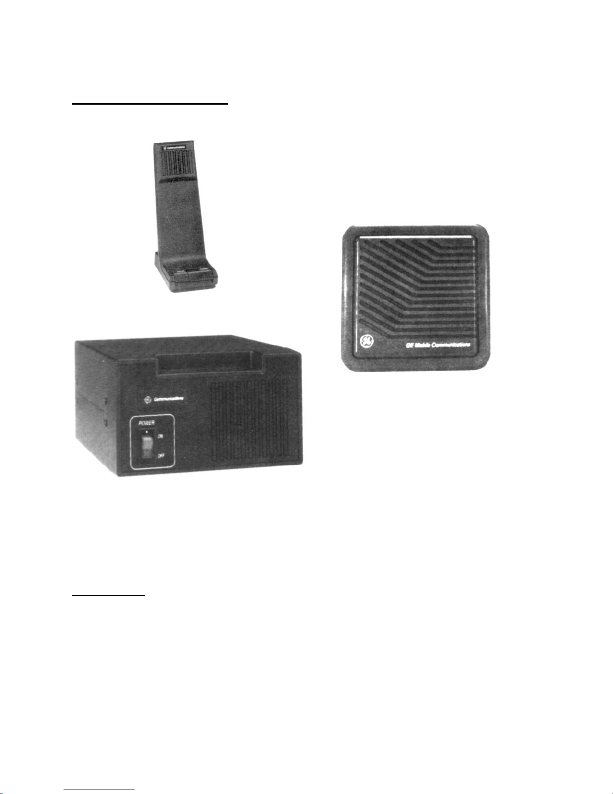
OPTIONS AND ACCESSORIES
CONTROL STATION OPTIONS:
Desk Microphone MGMC5H
Power Supply MGPS5V
NOT SHOWN:
Antenna - MGAN1A
Relay Kit - MGSU1C
Noise Suppression Kit - MGPD1A
External Speaker MGZM7C
Page-4Nov. 94
MONOGRAM SERIES LBI-38865
UNPACKING
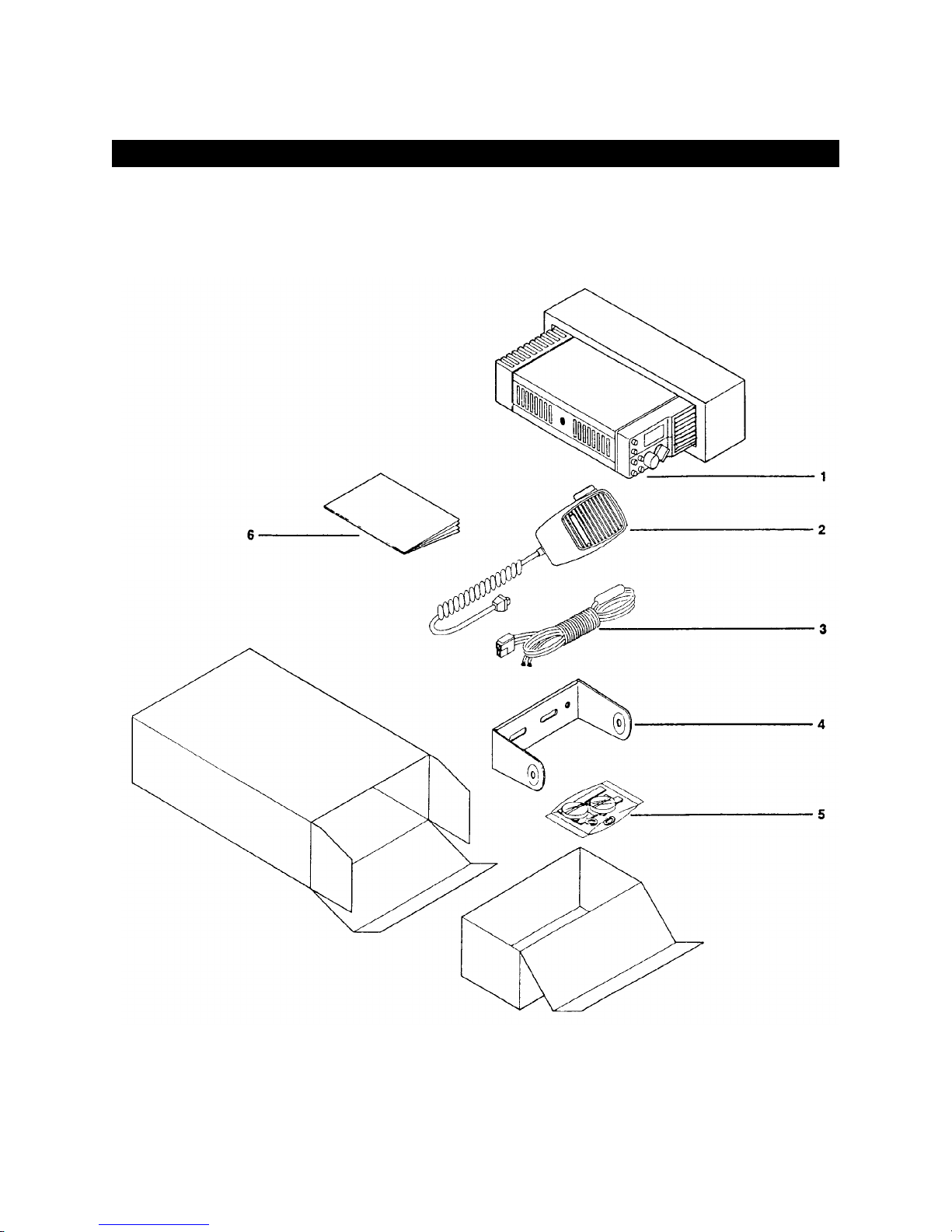
Check the carton and packing material carefully for the following items:
1. Transceiver Unit
2. Microphone
3. DC power cord
4. Mobile Mounting Bracket
5. Assembly Hardware
6. Operating Guide
Styrofoam not us ed
Inner Packing is now ca rdboard tray box.
UNPACKING
Figure 1 - Unpacking Diagram
Page-5Nov. 94

MONOGRAM SERIES LBI-38865
INTRODUCTION
INTRODUCTION
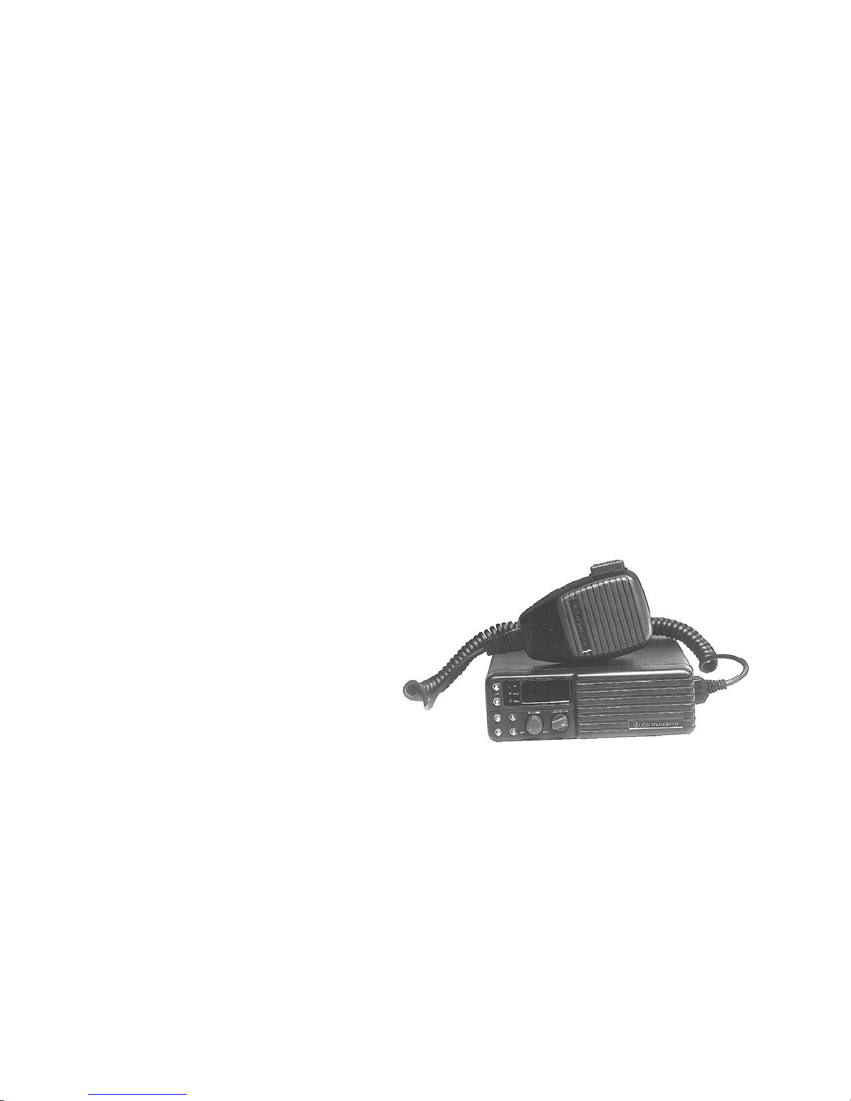
The Conventional Monogram Series Radio is a rugged two-way FM mobile radio which operated in the 400-440
MHz, 450-470 MHz or the 470-512 MHz band split. The Monogram is a synthesized radio utilizing microcomputer
technology to provide reliable high quality simplex two-way mobile communications. Its transmitter output power
level is 40 watts over the wide bandwidth, with an allowable 10 MHz maximum receive channel separation. The
basic radio package includes the following features:
Microprocessor Control
∗
Synthesized RF Channel selection (frequency control)
∗
Vacuum Fluorescent Channel Selection Display
∗
Channel Guard (CTCSS) Encode/Decode
∗
Digital channel Guard (DCG) Encode/Decode
∗
Priority Scan
∗
±
5 PPM frequency stability
∗
Field Programmable with PC
∗
Variable Squelch
∗
Internal 5-watt Speaker, with volume control
∗
Side Mounted Microphone Connector
∗
Rear Mounted Antenna Connector (SO-239)
∗
Rear power connections
∗
The small size of the Monogram radio makes it ideal for front mounting in conventional vehicles. The radio is
operated with a simple hand held microphone in combination with the operating controls described in the following
section.
Page-6Nov. 94
MONOGRAM SERIES LBI-38865
DESCRIPTION OF CONTROLS
DESCRIPTION OF CONTROLS
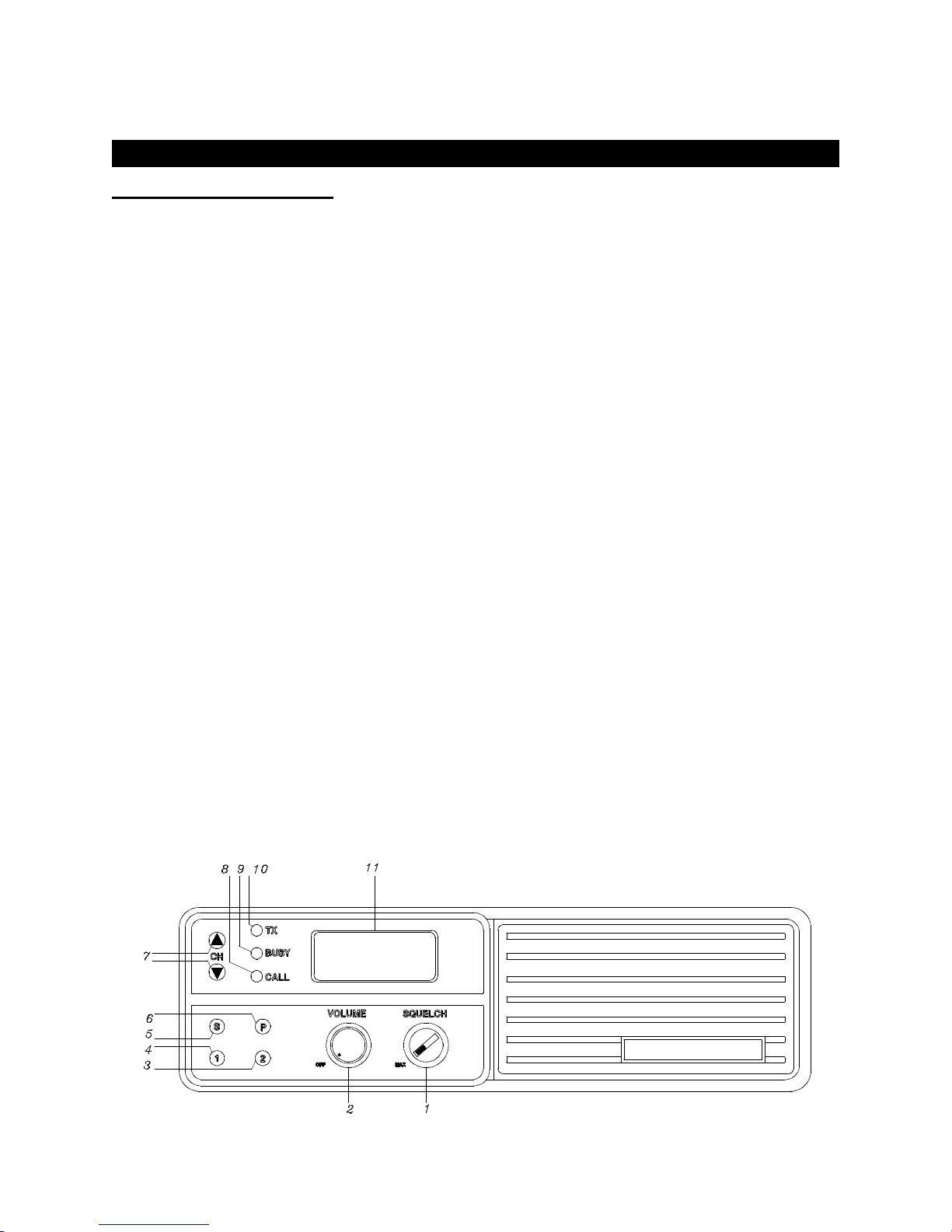
FRONT PANEL CONTROLS
1. Squelch Control: The squelch control will silence the receiver when no signal is being received.
2. ON/OF/VOLUME Control: This is the main power switch and volume control.
3. Monitor Button (2): This button performs three functions:
a. Disables tone or digital squelch options when in receive mode.
b. Returns to normal radio operation from the programming mode.
c. Controls display intensity.
4. Auxiliary Speaker Button (1): This button silences the internal speaker and connects the auxiliary speaker
(requires the auxiliary option printed circuit board to be installed). It also deletes channels from the scan list
while in the programming mode.
5. SCAN Push Button (S): This button turns the scan function "ON" (indicated by a red backlight) and "OFF".
It also serves as the ENTER function during SCAN programming.
6. PRIORITY SCAN Push Button (P): This button turns the PRIORITY SCAN function "ON" (indicated by a red
backlight) and "OFF". It also provides access to the programming mode when the radio is turned on.
7. Channel Change buttons (CH): The channel change buttons allow the operator to scroll either up or down
through the programmed channels.
8. Call Light Indicator (CALL): This green Light Emitting Diode (LED) indicator illuminates to indicate
activity on the channel during receive when coded squelch or digital signaling options are used.
9. Busy Channel Indicator (BUSY): This yellow Light Emitting Diode (LED) indicator illuminates to indicate
activity on the channel during receive.
10. Transmit LED Indicator (TX): This red Light Emitting Diode (LED) indicator illuminates during transmit
mode. It also will flash to indicate that the synthesizer is out of lock.
11. Channel Display: The front panel display indicated channel number, priority scan numbers, programming
mode and error messages.
FIGURE 2 - Front Panel Controls
Page-7Nov. 94
MONOGRAM SERIES LBI-38865
DESCRIPTION OF CONTROLS
BACK PANEL CONNECTORS
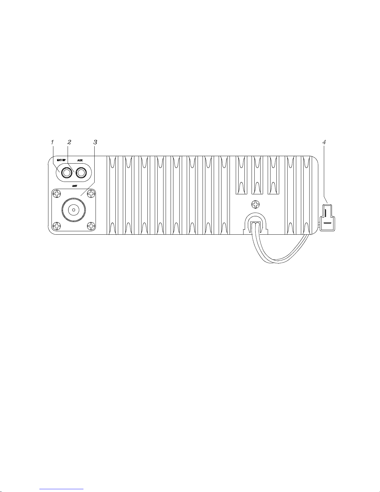
1. External Speake r Co nnector: This 3.5mm di a meter jack is provide d fo r a 4 oh m external speaker. The
internal speaker is silenced when the external speaker is connected.
2. Auxiliary Speaker Connector: This 3.5mm diameter jack is provided for an auxiliary speaker (Option
MGSU1C Relay Kit is required).
3. Antenna Connector: An SO-239 type connector. The output load must be 50 ohms.
4. DC 13.8V Connector: Polarized plug for 13.8 VDC power input - FOR NEGATIVE GROUND SYSTEMS
ONLY.
FIGURE 3 - Back Panel Controls
Page-8Nov. 94

MONOGRAM SERIES LBI-38865
OPERATION
OPERATION
• NOTE: The following description briefly outlines the operation of your UHF synthesized mobile radio. Consult
the operators manual for a complete description of all the modes of operation for which the radio is capable.
RADIO ON/OFF, POWER UP
1. Turn the radio on by turning the VOLUME control one-half turn clockwise. After 4000 appears in the
display and the power up alert tone is generated, the display will change to the #1 priority channel. If no
priority channel has been programmed, the display will change to channel 1.
2. Turn the radio off by rotating the VOLUME control fully counter-clockwise.
RECEIVING A CALL
1. Turn the radio on and select the desired channel.
2. Depress the monitor button (2) if necessary to illuminate it’s backlight. Adjust the volume control to a
comfortable listening level.
3. Rotate the SQUELCH control clockwise until the squelch noise (rushing sound) is no longer present.
4. Depress the MONITOR button (2) to extinguish the blacklight.
• NOTE: If the radio is equipped with coded squelch options, depress the MONITOR button (2) to enable the
option; the CALL indicator will no longer be illuminated.
TRANSMITTING
1. Turn the radio on and select the desired channel.
2. Pick up the microphone and listen briefly to insure the channel is clear. Alternatively, leave the microphone
on-hook and depress the MONITOR button (2).
3. Depress the PTT switch on the side of the microphone. Hold the microphone one to two inches from the
mouth and speak in a normal tone of voice. The TX indicator should be illuminated.
4. Release the PTT switch when the message is completed.
Page-9Nov. 94
MONOGRAM SERIES LBI-38865
OPERATION
DIGIT AL CHANNEL GUARD
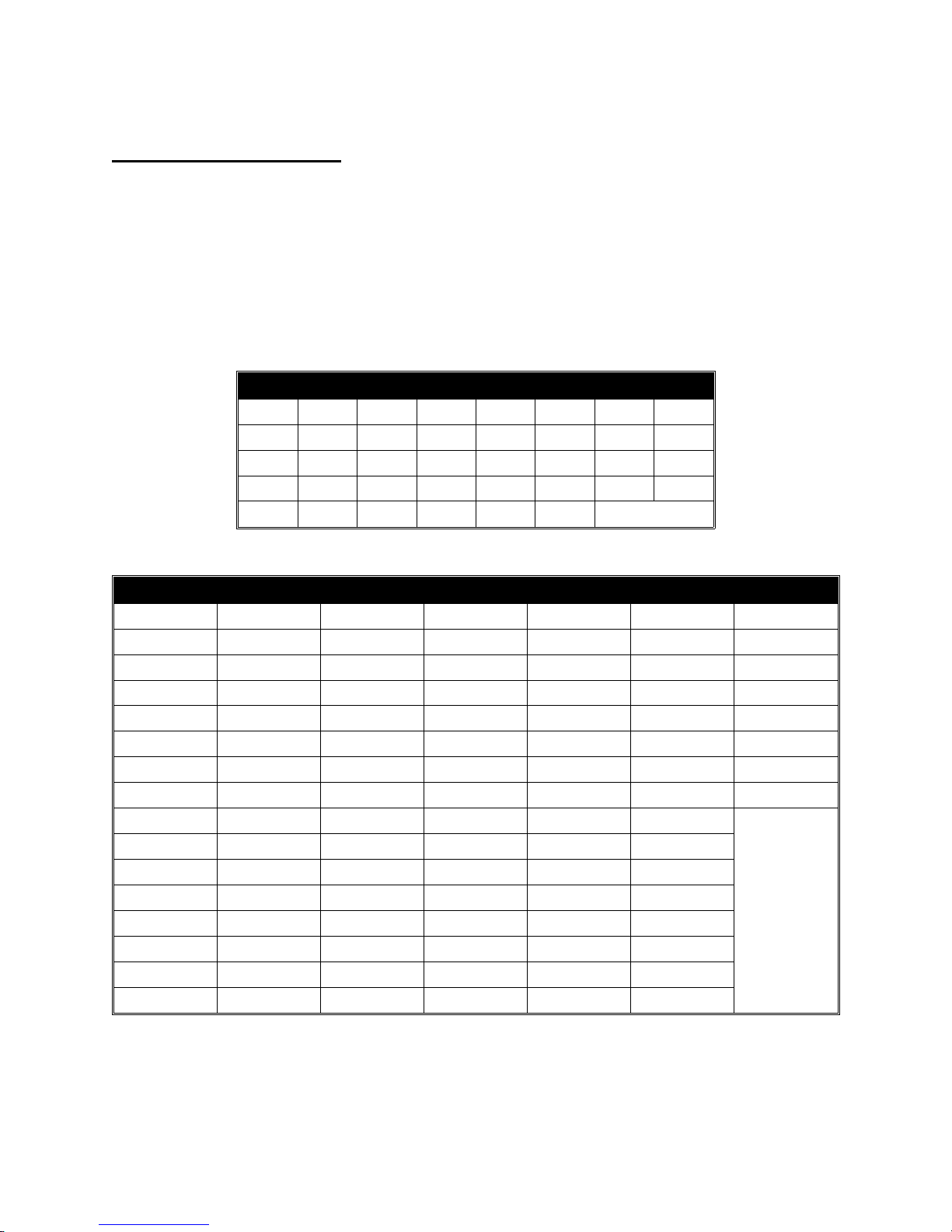
Channel Guard provides a means of restricting calls to specific radios through the use of a continuous tone coded
squelch system (CTCSS), or a multi-code digital squelch system (DCG). tone frequencies range from 67Hz to
250.3Hz. There are 83 standard programmable digital codes .
The Channel Guard tone fr eq uencies and codes are software programmable. Both tone frequencies and digital co des
may be mixed on eac h ch an nel. The frequenci es an d co des are shown in Tables 1 an d 2. A Channel Number displa y
that does not flash, indicates that Channel Guard is enabled, or that Channel Guard is not programmed. A flashing
Channel Number indicates that Channel Guard is programmed and disabled.
Table 1 - Channel Guard tone Frequencies
Standard Tone Frequencies in Hertz
67.0 71.9 74.4 77.0 79.7 82.5 85.4 88.5
91.5 94.8 97.4 100.0 103.5 107.2 110.9 114.8
118.8 123.0 127.3 131.8 136.5 141.3 146.2 151.4
156.7 162.2 167.9 173.8 179.9 186.2 192.8 203.5
210.7 218.1 225.7 233. 6 241. 8 250.3
Table 2 - Primary DCS Codes
DIGITAL SQUELCH CODES
023 114 174 266 411 506 703
025 115 205 271 412 516 712
026 116 212 274 413 523 723
031 122 223 306 423 526 731
032 125 225 311 431 532 732
036 131 226 315 432 546 734
043 132 243 325 445 565 743
047 134 244 331 446 606 754
051 143 245 332 452 612
053 145 246 343 454 624
054 152 251 346 455 627
065 155 252 351 462 631
071 156 255 356 464 632
072 162 261 364 465 654
073 165 263 365 466 662
074 172 265 371 503 664
Page-10-
Nov. 94

MONOGRAM SERIES LBI-38865
CIRCUIT ANALYSIS
CIRCUIT ANAL YSIS
RECEIVER
RF Amplifier
Incoming signals from the antenna jack are routed backwards through the transmitter lowpass filter in PIN diode
switch D16. In receive mode, D16 conducts allowing a low impedance path through the diode to the receiver front
end circuitry. The receiver RF amplifier section is comprised of two bandpass filter sections separated by an
amplifier based around Q1. These two filters allow signals at or near the operating frequency to pass but provide
strong rejection of the mixer’s spurious response frequencies. The first filter section is a two pole design formed
around RF helical resonator T1 and the associated circuitry. This filter is followed by the RF amplifier transistor Q1.
This device with its low noise figure, yields good receiver sensitivity while showing strong resistance to overload
from strong signals. The output of Q1 drives a pole filter section formed around T2 and T3. The output of the RF
amplifier stage is routed to the first mixer.
First Mixer and First IF Amplifie r
The action of the first mixer transistor Q2 is to convert incoming signals at the operating frequency to the frequency
of the first IF which is 21.4 MHz. the output of the mixer is at a frequency which is equal to the difference between
the frequency of the incoming signal and the local oscillator. In this radio, the local oscillator signal is chosen to be
21.4 MHz below the operating frequency. The device chosen to perform the mixing operation is Q2, a high
performance JFET. The incoming signal is applied to the gate of Q2 while the local oscillator is applied to the drain.
The local oscillator signal is filtered by Helical Resonator T6 and associated circuitry before being supplied to the
drain of Q2. The difference frequency signal at 21.4 MHz exits the mixer at the source of Q2 and is tuned for 21.4
MHz by T8, which drives the first IF filter XF1 and XF2. XF1 and XF2 form a 4-pole monolithic crystal filter pair
which in part determines the selectivity of the radio. The output of the crystal filter is routed to the first IF amplifier
formed around Q3. RF transformer T9 provides proper matching of the crystal filters to insure good bandpass
response and selectivity.
Second Mixer, Second IF, and FM Detector
The output of Q3 is applied to the input (pin 16) of IC2. IC2 is a single conversion FM receiver on one integrated
circuit chip. The signal at the input is routed straight to a mixer which converts the incoming signal to the second IF
frequency of 455 kHz. The second local oscillator is formed with crystal X1 and circuitry within IC2. The output of
the second mixer is at pin 3 which is connected to a ceramic bandpass filter CF1 and centered at 455 kHz. This filter,
along with XF1 and XF2, determine the adjacent channel selectivity of the radio. The output of CF1 drives a high
gain IF amplifier chain internal to IC2 which in turn drives the quadrature detector. The output of the detector is
amplified and exits IC2 at pin 9.
Audio
Detected audio from IC2 passes through a lowpass filter formed around L16, C64 and C65 which removes IF
frequency components at 455 kHz. the audio signal then passes through buffer amplifier transistor Q7 before being
filtered by a two section, 4-pole high pass filter (IC3). This filter removes DCS and CTCSS low frequency tones
from the recovered audio. Transistors Q6 and Q108 act as switches around volume control VR2 to mute the audio
during squelched receive operation. The audio signal is finally routed to audio power amplifier IC103 and then to the
speaker.
Page-11-
Nov. 94

MONOGRAM SERIES LBI-38865
CIRCUIT ANALYSIS
Squelch
The presence of an RF carrier is determined by noting the level of ultrasonic noise at the detector output (pin9) of
IC2. When a carrier is present, the noise level drops. The audio at pin 9 of IC2 is filtered by a two-pole bandpass
filter formed around L17, L18, C68 and C69. This filter passes audio at and near an audio frequency of 50 kHz. This
frequency is high enough that voice audio and its harmonics will not cause improper squelch operation. The output
of the filter is routed to an amplifier internal to IC2. The output of the amplifier drives Q4. The DC voltage at the
detector output is amplified and filtered by Q4. The output of Q4 send its squelch signal to the microprocessor.
When the microprocessor determines that a valid carrier exists, it sends an unmute signal to the audio switch
transistors Q6 and Q108.
TRANSMITTER
Audio
The microphone audio is amplified, pre-emphasized and peak limited by circuits within IC113. The output of the
limiter is routed through RV4, the microphone deviation control. Input CTCSS and DCS signals are routed through
RV5, the CTCSS/DCS deviation control. Both signals are summed through a lowpass filter formed around IC114 to
remove high frequency components from the limiter which could cause channel splatter. When the microprocessor
enables the TX 8 volt supply, analog gate IC115 delivers the modulation signal to the VCO transistor Q115 by
changing the capacitance of D123 and D110.
RF Driver and Power Amplifie r
Diode D11 acts as a switch allowing the RF signal from the phase locked loop frequency synthesizer to pass through
the RF driver and power amplifier during transmit, but not during receive. Buffer amplifier Q10 amplifies the carrier
to the level needed by the driver amplifier stages. The driver amplifiers, of which the last 2 stages are gain controlled
by the automatic power control, drive the final amplifier stage formed around Q14. The final amplifier boosts the
carrier level to the power level set by the automatic power control. The carrier signal passes through the automatic
power control directional coupler, the RF output lowpass filter, and then is routed to the antenna connector.
Automatic Power Control
The automatic power control directional coupler samples a portion of the forward RF power output to determine the
RF level. Diode D15 rectifies this RF sample and produces a DC voltage which is proportional to the RF output
level. This DC signal is summed with the voltage set from the power output control RV3. This voltage is compared
with a voltage derived from the TX 8 volt supply and the difference is amplified by IC5. The output of the RF driver
is proportional to its supply voltage. This controls the DC output of Q9, which supplies Q12 and Q13 controlling the
output of Q14 over the range from 10 to 40 watts. This completes a negative feedback loop which results in constant
output power over supp ly vo l ta g e and temperature va riations.
FREQUENCY SYNTHESIZER
The phase locked loop (PLL) fr equency synthesizer sec tion is re spo nsibl e fo r generating the RF signal at the carrier
frequency during transmit and at the local oscillator frequency for the receiver during receive. A PLL functions by
comparing the output frequency of a voltage controlled oscillator (VCO) with a fixed frequency reference. An error
signal is generated which drives the control input of the voltage controlled oscillator to force its frequency to match
the reference. The PLL based frequency synthesizer has a digital fr equency divider inserted between the output of
the VCO and the frequency comparison circuitry. As this divider number is varied, the output frequency of the VCO
varies as well with a frequency step size equal to the reference frequency (6.25 kHz in this radio). This allows a large
range of frequencies to be generated with one well controlled oscillator signal, the reference.
PLL Integrated Circuit
IC118 contains most of the digital circuitry to form a PLL frequency synthesizer. This includes a reference
oscillator, programmable reference frequency divide r, a programmable variable frequency divider, a modulus con trol
Page-12-
Nov. 94

MONOGRAM SERIES LBI-38865
CIRCUIT ANALYSIS
counter, a phase/ fr equency comparato r an d a frequency lock dete c t or. The operation of this int egrated circuit is
controlled by the radio’s microprocessor through a serial data line.
Reference Oscillator
Crystal X2, varactor D122, a thermistor/resistor network and the oscillator stage of IC118 form a temperature
compensated 12.8 MHz oscillator. This frequency is divided by 2048 to generate the 6.25 kHz frequency for the PLL
frequency synthesizer. This reference determines the frequency stability of the overall radio.
Voltage Controlled Oscillator
Transistor Q115 and its associated circuitry form a voltage controlled oscillator which is voltage tuned and band
switched by varactor diodes D12 3 and D110. the VCO output is buffer ed and isolated by Q117, Q118 and Q119.
Audio modulation is applied to the cathodes of D123 and D110 to produce frequency modulation during transmit.
Dual Modulus Prescaler
The internal dividers within IC118 are not able to operate at the VCO output frequency. To alleviate this problem,
part of the overall frequency division necessary between the VCO and the phase/frequency comparator is placed
external to, and controlled by, IC118. IC117 divides the VCO frequency by 128 or 129, determined by the state of
IC118 pin 6. This produces a lowe r frequency which can be further divided by IC108. By strategic timing when to
divide by 128 or 129, the overall division will be that necessary to put the VCO on the correct frequency.
Loop Filter
Resistors R317 through R322 and capacitors C291, C294 and C295 form the loop filter. The purpose of the loop
filter is to filter out the 6.25 kHz reference frequency products from the output of phase/frequency comparator IC118
and to determine the dynamic operation of the overall loop.
R316, C289, Q113 and Q114 act to speed up operation of the synthesizer loop during channel changes and during
frequency transition (receive to transmit and transmit to receive).
Out-of-Lock Detector
IC118 contains a cir cu i t whi ch c om pa res the timing difference of the 6.25 kHz reference frequency and the divided
down VCO frequency. The output is a 6.25 kHz pulse whose duration is equal to the timing difference. R306 and
C274 filter this pulse and average it producing a DC voltage which is proportional to the pulse width. When the loop
is in lock, this voltage is zero, but when the loop is out of lock, it rises to a level which will forward bias Q112. The
output of Q112 drives the microprocessor. The microprocessor will not allow the radio to transmit unless the
synthesizer is in lock. This is to prevent out of band signals from being transmitted.
Page-13-
Nov. 94

MONOGRAM SERIES LBI-38865
PREVENTIVE MAINTENANCE
PREVENTIVE MAINTENANCE
To ensure high operating efficiency and to prevent mechanical and electrical failures from interrupting system
operations, routing checks should be made of all mechanical and electrical parts at regular intervals. Preventive
maintenance should include the following checks:
CONNECTIONS
Ground connections to the voltage source should be peri odically checked for tightness. Loose or poor connections to
the power source will cause excessive voltage drops and faulty operation. When ground connections are not made
directly to the batter, the connection from the battery to vehicle chassis must be checked for low impedance. A high
impedance may cause excessive voltage drops and alternat or noise problems.
ELECTRICAL SYSTEM
Check the voltage regulator and alternator or generator periodically to keep the electrical system within safe and
economical operation limits. Over voltage is indicated when the battery loses water rapidly. Usage of 1 or 2 ounces
of water per cell per week is acceptable for batteries in continuous operation. A weak battery will often cause
excessive noise or faulty operation.
MECHANICAL INSPECTION
Since mobile units are subject to constant shock and vibration, check for loose plugs, nuts, screws and other parts to
make sure that nothing is working loose.
ANTENNA
The antenna, antenna base and all contacts should be kept clean and free from corrosion. If the antenna or its base
should become coated or poorly grounded, loss of radiation and a weak signal will result.
ALIGNMENT
The transmitter and receiver meter readings should be checked periodically, and the alignment "touched up" when
necessary. Refer to the Alignment Procedure in this Service Manual.
FREQUENCY CHECK
Check the transmitter frequency and deviation. Normally, these checks are made when the unit is first put into
operation, after the first six months, and once a year thereafter.
Page-14-
Nov. 94

MONOGRAM SERIES LBI-38865
DISASSEMBLY
DISASSEMBLY
TOP AND BOTTOM COVERS
There are no screws used to secure the top and bottom covers. Both top and bottom covers are removed with a flat
blade screwdriver or similar tool. On each side of the radio there are t wo small slots (on e at the top and one at the
bottom). Insert the screwdriver into the slot and gently pry the lip of the cover out from the radio. without removing
the screwdriver from the slot and in the same motion, pry the cover up . Both covers can be rem ov ed f ro m eit h er side
of the radio.
FRONT PANEL
1. Remove the (6) M3 x 6 machine screws (3 on top and 3 on bottom) that secure the front panel to the chassis.
2. Two cables connect the volume board to the RF board (at PL1) and to the digital board at (PL2). These
cables may be unplugged at the RF boa rd and at the digital board. A ribbon cable from the di splay board to
the digital board must be unplugged to remove front panel.
RF BOAR D
1. Remove the (13) M3 x 24 machines screws securing the RF shield to the chassis.
2. Remove the M3 x 8 machine screw that secures the DC cord bracket to the chassis. Slide the bracket and
cord out of the chassis.
3. Remove the (6) M3 x 6 machine screws (3 on top and 3 on bottom) that secure the front panel to the chassis.
4. Remove the RF shield by pushing the front panel forward so the shield will clear and then sliding the DC
cord, bracket and connector through the rectangular hole in the shield.
5. De-solder the antenna connector from the RF board.
6. Remove the remaining (10) machine screws securing RF board, IC1, and Q14 and Q9.
7. Q13 is mounted to the chassis with a spanner nut which is only accessible from top of the radio through a
hole in the digital board. Remove the spanner nut.
8. Remove the RF board.
Page-15-
Nov. 94

MONOGRAM SERIES LBI-38865
DISASSEMBLY
DIGITAL BOARD
1. Remove the (6) M3 x 18 machine screws that secure the top panel shield to the chassis.
2. Unplug and remove the Auxiliary Relay PCB at PL5.
3. Remove the (6) machine screws (3 on top and 3 on bottom) that secure the front panel to the chassis.
• The following steps detail the removal of the RF shield which is necessary before continuing with the removal
of the digital board.
4. Remove the (13) M3 x 24 machine screws securing the RF shield to the chassis.
5. Remove the M3 x 8 machine screw that secure the DC cord bracket to the chassis. Slide the bracket and
cord out of the chassis.
6. Remove the RF shield by pushing the front panel forward so the shield will clear and then sliding the DC
cord, bracket and connector through the rectangular hole in the shield.
7. Unplug the VCO cable from the jack.
8. Remove the remaining (10) screws securing the digital board, IC5, IC6 and IC104 to the chassis.
9. The digital board can now be removed from the chassis, however the front panel assembly is still attached b y
two cables (on e fr om th e Cont rol boar d and one from t he displ ay b oard ). T he cable from the Control board at PL2
may be unplugged. The ribbon cable from digital board may be unplugged at FLT.
Page-16-
Nov. 94

MONOGRAM SERIES LBI-38865
PROGRAMMING INSTRUCTION
PROGRAMMING INSTRUCTION
The UHF synthesized mobile radio is equipped with a personality EEPROM. All customer information such as the
customer frequencies, custome r tones and customer options are stored in the EEPROM. The EEPROM cont ains all
information to tailor the operation of the radio to the user’s requirements. The EEPROM is programmed by using an
IBM compatible pers on al co mp ut er with MSDOS, Programming Cable TQ-3376 and Pro gr amming software
TQ-3375.
PROGRAMMING THE RADIO
The Programming Ca ble TQ-3376 is a Y-cable . The base of the "Y" has a standard 25 pin connector whic h pl u gs
into the computer, the remaining end has a 6 pin connector which fits into the connector PL1 on the digital board
inside the radio. To use this cable, remove the top cover of the radio as described in the DISASSEMBLY section.
Plug the six pin connector into the socket inside the radio (PL1), which is located near the EEPROM IC107. Plug the
base of the "Y" into the computer that will program the radio. See the diagram in TQ-3375 Software Manual. In
order to program the radio with the programming cable, it is necessary to put the radio into the programming mode.
To do this, press the P "PRIORITY" button/LED on the radio and turn the radio ON. The radio will sound a prompt
tone and show the words "PROG" on the display. Please refer to the Software Manu al fo r fu rther instructions on the
operation of the Programming Software. After completing the programming instructions in the Manual, remove the
cable from PL1 and replace the cover on your UHF synthesized mobile radio.
Page-17-
Nov. 94
 Loading...