

Ericsson LBI-31511B Maintenance Manual
LBI-31511B
Printed in U.S.A.
TABLE OF CONTENTS
Page
DESCRIPTION . . . . . . . . . . . . . . . . . . . . . . . . . . . . . . . . . . . . . . . . . . . Front Cover
INITIAL ADJUSTMENT . . . . . . . . . . . . . . . . . . . . . . . . . . . . . . . . . . . . . . Front Cover
MAINTENANCE . . . . . . . . . . . . . . . . . . . . . . . . . . . . . . . . . . . . . . . . . . 1
PREVENTIVE MAINTENANCE . . . . . . . . . . . . . . . . . . . . . . . . . . . . . . . 1
DISASSEMBLY . . . . . . . . . . . . . . . . . . . . . . . . . . . . . . . . . . . . . . . . . 1
PA TRANSISTOR REPLACEMENT . . . . . . . . . . . . . . . . . . . . . . . . . . . . . 2
REMOVING IC’s . . . . . . . . . . . . . . . . . . . . . . . . . . . . . . . . . . . . . . . . 2
REPLACING CHIP COMPONENTS . . . . . . . . . . . . . . . . . . . . . . . . . . . . . 2
PROGRAMMING AND ALIGNMENT . . . . . . . . . . . . . . . . . . . . . . . . . . . . . . 2
SERVICE TIPS . . . . . . . . . . . . . . . . . . . . . . . . . . . . . . . . . . . . . . . . . . . . 3
TEST AND TROUBLESHOOTING PROCEDURES . . . . . . . . . . . . . . . . . . . . . . . 4
TRANSMITTER ALIGNMENT . . . . . . . . . . . . . . . . . . . . . . . . . . . . . . . . 7
RECEIVER ALIGNMENT . . . . . . . . . . . . . . . . . . . . . . . . . . . . . . . . . . . . . 11
RECEIVER AUDIO AND SQUELCH WAVEFORM CHECKS . . . . . . . . . . . . . . . . . . 14
MECHANICAL LAYOUT . . . . . . . . . . . . . . . . . . . . . . . . . . . . . . . . . . . . . 15
INTERCONNECTION DIAGRAMS . . . . . . . . . . . . . . . . . . . . . . . . . . . . . . . . 17
MAINTENANCE MANUAL
403-430 MHz & 450-512 MHz, DELTA-S NARROWBAND
TWO WAY FM RADIO
SERVICE SECTION
DESCRIPTION
The service section of this m anual co ntains th e diagnostic
routines, and other maintenance information to service this
radio. The service section includes:
• System interconnections.
• Mechanical layout.
• Disassembly procedures.
• Replacement of IC’s chip cap aci tors a nd resistors.
• Alignment procedures for the transmitter and re-
ceiver.
• Troubleshooting flow charts and waveforms .
INITIAL ADJUSTMENT
After the radio has been installed (as described in the
Installation Manual), the following adjustments should be
made by a certified electronics technician.

TRANSMITTER ADJUSTMENT
The adjustment for the transmitter includes measuring the
forward and reflected power and adjusting the antenna length for
optimum ratio, then setting the transmitter to rated power output.
Next, measure the frequency and modulation and record these
measurements for future reference. For th e complete t ransmitte r
adjustment, refer to the Alignment Procedure (see Table of
Contents).
MAINTENANCE
PREVENTIVE MAINTENANCE
To ensure high operating efficiency and to prevent mechanical and electrical failures from interrupting system operations,
routine checks should be made of all mechanic al and elect rical
parts at regular inter vals. This preve ntive maintenance should
include the checks as listed in the table of Maintenance Checks.
DISASSEMBLY
• To gain access to t h e unit for servicing:
1. Unlock the radio.
2. Pull down the handle.
3. Pull th e r adio f o rwa rd and lift radio out of mounting
place -- if desired.
4. Pry u p the front of top cover and lift the cover off.
5. To gain access to the bottom side, pull the radio all
the way out of the mounting frame and remove the
four mushroom shaped feet using a #30 Torx® s c r e w driver.
• To remove the TRS board:
1. Remove the bottom cover.
2. R emove the el even retaining screws at (A) (Figure 1)
securing the circuit board to the main frame.
3. Remove two retaining screws (B) securing systems
connector J601 to front casting.
4. Unsolder the two feed through capacitor termina ls
(E) on printed wire pattern.
5. Turn over the radio and remove the three retaining
screws (D) (Figure 2) securing t he au dio b rid ge a m plifier, U601 and U602, and the 5 and 9 volt regulators U702 and Q705 to the side of chassis.
6. To remove the front end shield, remove the 20 retaining screws securing the shield to the front end c asting
and remove.
7. To remove the synthesizer shield, remove the seventeen retaining screws securing the shield to the synthesizer top casting.
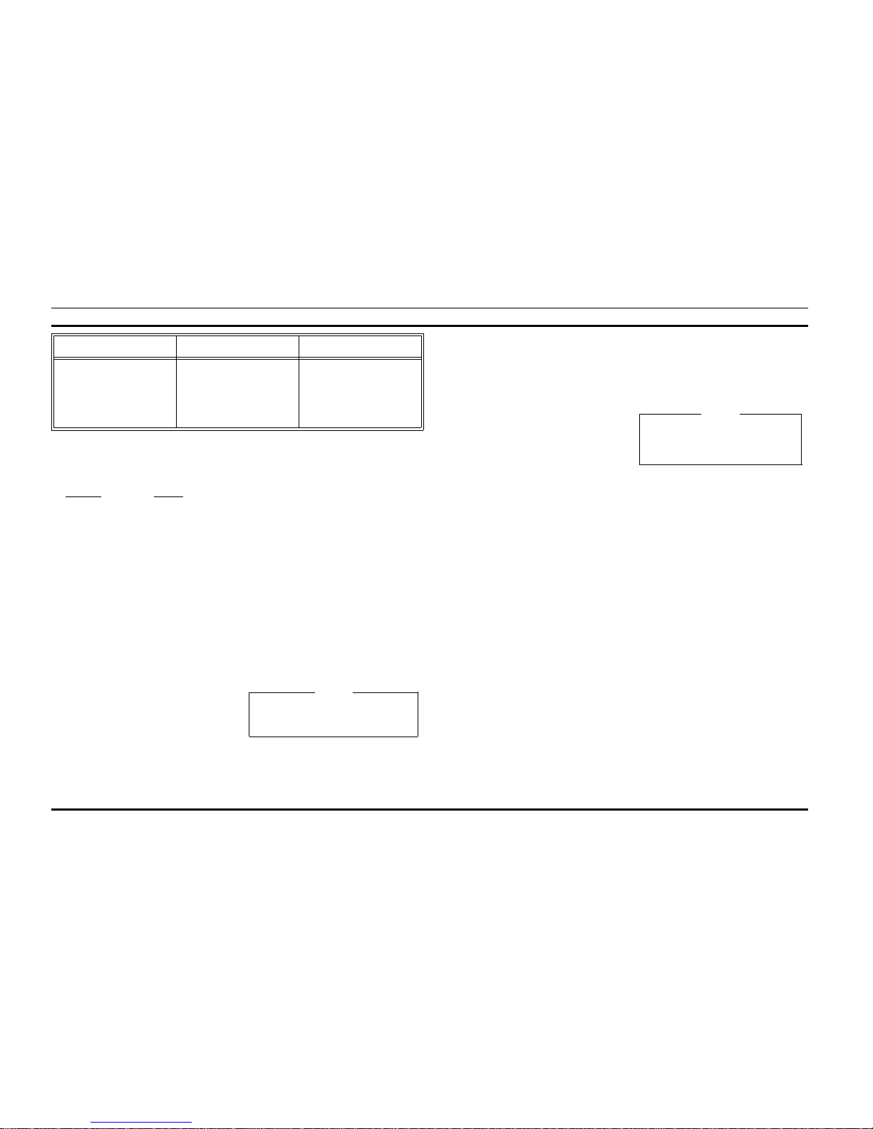
MAINTENANCE CHECKS
INTERVAL
6 Months
As
Required
CONNECTIONS - Ground connec tions and conn ections t o the vo ltage source should be periodically
checked for tightness. Loose or poor connections to the power source will cause excessive voltage
drops and faulty operation. When ground connections are not made directly to the battery, the
connection from the batte ry to vehicle chassis must be c hecked f or low impe dance. A h igh imped ance
may cause excessive voltage drips and alternator noise problems.
X
ELECTRICAL SYSTEM - Check the voltage regulato r and alternato r or generator pe riodically to
keep the electrical system within safe and economical operating limits. Overvoltage is indicated when
the battery loses water rapidly. Usage of 1 or 2 ounces of water per cell per week is acceptable for
batteries in continuous operation. A weak battery will often cause excessive noise or faulty operation.
X
MECHANICAL INSPECTION - Since mobile units are su bject to constant shock and vibration, check
for loose plugs, nuts, screws and parts to make sure that nothing is working loose. Be sure that all
screws are properly torqued.
X
ANTENNA - The antenna, antenna base and all contacts should be kept clean and free from dirt or
corrosion. If the antennas or its base should become coated or poorly grounded, loss of radiati on a nd
a weak signal will result.
X
ALIGNMENT - The tra nsmi t te r a nd receiver meter rea d ings should be checked periodically, and the
alignment "touched up" when necessary. Refer to applicable Alignment Procedur e and troubleshooting sheet for typical voltage readings.
X
FREQUENCY CHECK - Check transmitter frequency and deviation. Normally, these checks are
made when the unit is first p ut into o p er ation, after the first six months an d on ce a y ear thereafter.
X
Copyright© September 1985, General Electric Company
NOTE
With the top cover removed all components on the
PA and TRS board are accessible for t uning. The PA,
IF, and synthesizer/exciter covers must be removed
to expose components.
Figure 1 - Disassembly - Bottom View
Figure 2 - Disassembly - Top View
LBI-31511 LBI-31511
1
• To replace TRS board:
1. Perform above procedures in reverse order.
• To remove the PA board:
1. Remove the three retaining screws (G) securing the
PA filter cover to the main frame.
2. Remove the eight retaining screws (F) from around
the edge of the PA board.
3. Remove the two retaining screws (H) securing the
antenna connector to the main frame.
4. Loosen the retaining screw (J) securing the pass
transistor to the side of the PA chassis compartment.
5. Remove the retaining screws (K) securing the PA
transistors to the main frame.
6. Turn the radio over and remove the nut and washer
from the stud of PA transistor Q1.
7. Unsolder the two power feed through capacitors at
(L).
8. C arefu lly lift the PA board up off th e pins extend ing
upward from the TRS board.
• To replace the PA board:
1. P erform the ab ove proced ures in r everse o rder, bei ng
careful to realign all interconnecting pins and
sleeves. Be sure the antenna gasket between the
antenna jack and front casting is positioned properly.
PA TRANSISTOR REPLACEMENT
• To replace the PA RF transistors:
1. Unsolder one lead at a time with a 50 watt soldering
iron. Use a scribe o r X-acto® knife to hold the lead
away from the printed circuit board until the solder
cools.
2. Remove retaining screws and lift out the transistor.
Remove any old solder from the printed circuit board
with a vacuum desoldering tool. Special care should
be taken to prevent damage to the printed circuit
board runs because part of the matching network is
included in the base and collector runs.
3. Trim t he new transistor le ads ( if require d) to the lead
length of the removed transistor. The letter "C" on
the top of the transistor also indicates the collector.
4. Apply a coat of silicon grease to the transistor mounting surface. Place the transistor in the mounting hole.
Align the leads as shown on the Outline Diagram.
Then replace the transistor mounting screws using
moderate torque.
5. Solder the leads to the printed circuit pattern. Start at
the inner edge of mounting hole and solder the remaining length of t ransisto r lead to the b oard. Use
care not to use excessive heat th at cau s es the printed
wire board runs to lift up from the board. Check for
shorts and solder bridges before applying power.
REMOVING IC’s
Removing IC’s (and most other soldered-in components)
can be easily accomplished by using a vacuum desoldering tool.
To remove an IC, heat each lead s eparately on the solder side and
remove the old solder with the desoldering tool.
REPLACING CHIP COMPONENTS
Replacement of chip components should always be done
with a temperature-controlled soldering iron, using a controlled
temperature of 700°F (371°C). However, do NOT touch black
metal film of the resistors or the ceramic body of capacitors with
the soldering iron.
To Remove Chip Components
1. Grip the component with tweezers or needle nose pliers .
2. Alternatel y heat each en d of the chip i n rapid succession
until solder flows, and then remove and discard the
chip.
3. Remove excess solder with a vacuum solder extractor.
4. Carefully remove the epoxy adhesive and excess flux
to prevent damage to the printed board.
To Replace Chip Components
1. Using as little solder as possible, "tin" one end of the
component and one of the pads on the printed wiring
board.
2. Place the " tinned" end of th e component on the "tinned"
pad on the board and simultaneously touch the component and the pad with a well "tinned" soldering iron
while pressing the component down on the board.
3. Place the "tinned" soldering iron on the other end of the
component and the pad simultaneously. Apply solder
to the top of the end of the component until the solder
starts to flow. Use as little solder as possible while
getting a good joint.
4. After the component has cooled, remove all flux from
the component and printed wiring board area with
alcohol.
PROGRAMMING AND ALIGNMENT
The following procedure describes how to change the frequencies in the radio EEPROM(S) for new user frequencies.
Also included is an alignment procedure guide to assist you in
aligning the radio after the frequencies have been changed. The
alignment procedure should be performed in the order given and
it
must be performed prior to putting the radio back in service.
PROGRAMMING
The DELTA-S UHF Narrowban d radio may be programmed
using the TQ-2310 Suitcase Programmer, the 4EX22A10 Hand
Programmer or by a Personal Computer. The procedures for
using the programmers are covered in detail in LBI-31263 (TQ-
2310) and LBI-31275 (4EX22A10). TQ-3334 provides t he software and programming instructions for programming with a PC.
When programming the radio, considerat ion m ust b e g iv en
to the individual band split for the T/R/S board. See the Programming tips on the following page and the individual band splits
listed below.
NOTE
Torque #8 nut on Q1 to 6 inch pounds when replacing.
NOTE
Note the position of the copper washer spacer under
transistor Q1. Be sure that this spacer is in place when
replacing the board.
Failure to solder the transistor leads as directed may
result in the generation of RF loops that could damage
the transistor r may cause low power output.
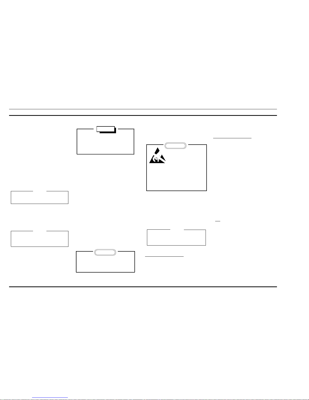
CAUTION
The RF Power Transistors used in the transmitter
contain Beryllium Oxide, a T OXIC substance. If the
ceramic or other encapsulation is opened, crushed,
broken or abraded, the dust may be hazardous if
inhaled. Use care in replacing transistors of this type.
WARNING
The CMOS Integrated Circuit devices used in this equipment can be
destroyed by static discharges. Before handling one of these devices,
the serviceman should discharge
himself by touching the case of a bench test instrument that has a 3-prong power cord connected to an
outlet with a known good earth ground. When soldering or desoldering a CMOS device, the soldering iron
should also have a 3-prong power cord connected to
an outlet with a known good earth ground. A batteryoperated soldering iron may be used in place of the
regular soldering iron.
CAUTION
NOTE
The metallized end terminations of the parts may be
touched with the soldering iron without causing damage.
LBI-31511 LBI-31511
2
MICROCOMPUTER SOFTWARE (U705)
The latest software package is a 19A703244P23 or a
19A703868G5; replacing the following packages:
Narrowband Wideband
19A703244P10 19A703244P21,22
19A703241G3-8 19A703868G2-4
PROGRAMMING TIPS
When programming with the Suitcase Programmer or a
Personal Co mputer, Jumper P707 (if present on Negative
Ground System Boards only) must be r emoved. I f programmi ng
the S950/S990 Control Unit for download to the radio, P703 o n
the rear of Control Unit must be disconnected to isolate Advance
Change Pulse Line.
When the 4EX22A10 Hand Programmer, Jumper P706
(Negative Ground T/R/S Boards) must be removed (to disconnect D720), or lift one end of D720 on Floating Grd T/R/S
Boards.
ALIGNMENT
After the radio has been programmed with new us er frequencies, the radio re-alignment procedure is as follows:
UNDER SYNTHESIZER AND TRANSMITTER
ALIGNMENT PROCEDURE
1. Check 9 volt regulator.
2. Ad just t he synthesizer trans mitter VCO.
3. Ad just t he synthesizer recei v er VCO.
4. Tune the exciter.
5. A d just t ra nsmi tte r po wer a mp li fi er.
6. Set the reference oscillator frequency (one setting for
both transmit and receive).
UNDER RECEIVE ALIGNMENT SECTION
1. Ad just l ocal oscillato r-buffe r inject ion.
2. A d j ust f r ont e n d.
3. A djust IF s ele cti vi ty.
4. A d just FM de tec to r/ aud io pr e- am p.
SERVICE TIPS
CHANNEL GUARD BOARD
When servicing the transmit/receive/synthesizer board it
may be helpful to remove and relocate the Channel Guard board.
Both the Channel Guard board and Channel Guard extender may
be removed and set aside during servicing. While servicing the
radio install P608 to connect VOL/SQ/HI.
MICROCOMPUTER
When servicing the microcomputer/synthesizer circuitry
it is sometimes desirable to force the microcomputer into
specific operating modes. Following are some tips that allow
you to initiate these modes.
• To force the microcomputer to continually try to
reload the synthesizer. This mode will enable you to
check the serial data, clock, channel change pulse and
enable signals to the synthesizer. Grounding the lock
detect line into the microcomputer at U703-8.
• To stop the microcom puter from running, disable the
watchdog timer by shorting the collector and emitter
of Q714 and ground the sing le step l i ne a t U705-5.
MICROPHONICS
Synthesized radios tend to be sensitive to shock and
vibration, creating microphonics. The construction of the
DELT A-S, r adio with its die ca st aluminum frame, cast shields,
and multiple board mounting screws, provides a high degree
of immunity. When removing either printed circuit board or
the shields, note the exact location and position of all mounting
hardware including rubber padding and bracket (if included).
When servicing th e ra dio be sure tha t n o sol der bui ldup
has occurred on the chassi s or sh i eld.
To assure a high degree of resistance to microphonics be
sure to replace exactly, all hardware removed. Be sure that all
mounting screws are properly torqued and shields in place.
Refer to Mechanical Layout Diagram.
TEST FREQUENCIES
If the EEPROM is not cu stom progr ammed to the c ustomers specified personality, then a standard test program is provided. The EEPROM is programmed on channels 1 through
16 including tone and digital Channel Guard and carrier control timer. Ta ble 1 identifies the programmed test frequencies.
BAND
SPLIT
T/R/S BOARD
(NEG. GRD. ONLY)
T/R/S BOARD
(FLOATING GRD.)
450-470 MHz
470-494 MHz
494-512 MHz
403-430 MHz
450-470 MHz
470-494 MHz
494-512 MHz
403-430 MHz
19D901620G1 (Tin Cont.)
19D901620G2 (Tin Cont.)
19D901620G3 (Tin Cont.)
19D901620G4 (Tin Cont.)
19D901620G5 (Gold Cont.)
19D901620G6 (Gold Cont.)
19D901620G7 (Gold Cont.)
19D901620G8 (Gold Cont.)
19D900920G1
19D900920G2
19D900920G3
19D900920G4
NOTE
Typical voltage readings are provided on the Schematic
Diagram for reference when troubleshooting.
NOTE
Loose or rubbing parts, especially in the VCO area
are particularly sensitive and can cause microphonics. Again be certain all h ardware is p roperly installed
and torqued.
LBI-31511 LBI-31511
3

TROUBLESHOOTING PROCEDURE
SIGNAL INDICATION VOLTAGE LEVEL
CAS
RUS
Sq Dis, Input
CCT Sq Dis, Input
TX Enable
PTT, Input
High Level
Low Level
High Level (RX Un-sq)
Low Level (RX Squelched)
Low Level (RX Mute/PTT)
Pulled low (RX unsquelched)
Logic Low (Sq. Dis)
Logic High (Sq)
RX Un-Sq
Logic Low
Logic High
Logic Low
Logic High
Logic Low
Logic High
9.0 Vdc
0.15 Vdc
9.0 Vdc
0.15 Vdc
0.6 Vdc
0 Vdc
2.4 Vdc
0.14 Vdc
0.35 Vdc
5.5 Vdc
2.0 Vdc
9.0 Vdc
1.0 Vdc
13 Vdc
CURRENT REFERENCE CHART
SERVICE
PLUG
FUNCTION TYPICAL CURRENT/mA
P701
P702
P703
P704
P705
5V
9V
9V
9V
9V
75
70
TX 90, RX 80
TX 45, RX 75
TX 40, RX 55
TEST POINT DATA (Typical)
TEST POINT VOLTAGE CONTROL DESCRIPTION
J602-3
9.0 ±0.05 Vdc
R703 9 Volt Regulator
J602-2 13.2 Vdc (A+)
J202 3.0-7.5 Vdc C220 (RX)
L209 (TX)
VCO Control Voltage
(See Synth Align)
J353 0.7 VPP Reference Osc. Output (high
impedance)
J352 5.5 Vdc (Nominal) Reference Oscillator
compensation line voltage
J712 5.0 Vdc VCC to Microcomputer
(Cont.)
TYPICAL PERFORMANCE INFORMATION
SIGNAL LEVELS
(Cont.)
TYPICAL PERFORMANCE INFORMATION
RADIO CONNECTOR IDENTIFICATION
Front Connector
Systems Metering
Option Connector
PROM Program Plug
RF Metering
RX Input
IF Input
RX Inj.
Exciter Input
Exciter Output
Hand Programmer Enable
Program Disable
TX PA Metering
VG Interface
Fixed Squelch
Channel Guard
Aux Audio
DPTT
IGN A+
J601
J602
J603
J711
J101
P401
P404
P451
P102
P101, P103
P706
P707
J1
P612
P605
P608
P610
P402
P403
TRANSMITTER QUICK CHECKS
– Connect red system metering plug to J602, system metering.
– Connect black plug of GE Test Set to RF Metering jack J101. Set polarity to "+" and voltage range to the 1 volt
position ( Te st 1).
EXCITER
RANGE
POSITION
RF METERING J101
EXCITER READINGS
PROBABLE CAUSE
METERING READINGS
TEST
POS.
METERING
JACK J101
FUNCTION
METER
SCALE
TYPICAL
READING
HIGH LOW
TEST 1 A J1 0 1- 10 AMPL-1 0-1 0.2V
Q101
Shorted
R101, R103
Open
Q101 Open; R103, R105,
Open; L103 Open;
Oscillator/ Buffer
Defective
TEST 1 B J101-9 TRIPLER 0-3 0.2V
Q102
Defective; R107
Open
Q102 Sho rt ed; R110 Op en;
L104, L105, and associat ed
circuits, defective or
improperly tuned.
TEST 1 C J101-8 AMPL-3
REL PWR
OUT
0-1 0.5V
Helical Coil
L114
Shorted Or
Mis-tun ed
Q103 OR Q104 defective.
Check resistors , capacitors
around Q103 and Q104.
Helical coils L107, L108
mis-tuned or defective.
D101 and associated
metering circuits defective.
RECEIVER READINGS SYSTEM JACK, J602
TEST POS FUNCTION SCALE
TYPICAL
READING
D IF AMP 1V 0.75
H RX INJ 1V 0.55
LBI-31511 LBI-31511
4
TROUBLESHOOTING PROCEDURE
NOTE
Regulated +5 Vdc and +9 Vdc can be opened by P701 thru P705 to facilitate troubleshooting.
POWER AMPL METERING J1
PA JACK READINGS
METER
READING
PROBABLE CAUSE
80, 90
100W
35, 40
50W
65,
75W
TEST
POS.
METERING
POINT
FUNCTION
MEASURED
SCALE
TYPICAL
READING
TYPICAL
READING
TYPICAL
READING
HIGH LOW
A J1-10 RF DRIVE 0-1 V 0.5 V 0 .5 V 0.5V
Low exciter output.
Realign or repair exciter.
B J1-9 CONTROL
VOLTAGE
0-15V 4 V 4.5 V 7.5V
Low exciter
output
High exciter output.
C J1-8 TX A+ 0-15V 12.5V 12.5V 12.5V
Exces sive volt age drop
in power ca b le .
E J1-6 PA
CURRENT
0-30A 15 A --- 11A
RF output
excessively
high. Be sure
antenna is
properly
matched to 50
ohms.
RF output low.
F J1-5 DRIVER
CURRENT
0-15A 5 A 8 A 4A
100 WATT
PA Che ck
A1Q5 and
A1Q6. Be
sure antenna
is properly
matched to 50
ohms.
100 WATT PA A1Q5
and A1Q6 ha ve
excessive gain. RF gain.
RF output set too low.
40 WATT PA
RF output
power is
excessive. Be
sure antenna
is properly
matched to 50
ohms.
40 WATT PA Low RF
output.
(Cont.)
PA QUICK CHECKS
– Connect red system metering plug to J602, system metering.
– Connect black plug of GE Test Set of RF Metering jack J1 of PA. Set polarity to "+" and voltage range to the 1 volt
position ( Te st 1).
(Cont.)
PA TROUBLESHOOTING PROCEDURE
When troubleshooting the transmitte r ch eck for t ypica l mete r readi ngs for t he ex cite r, J101, and the power amplifier JACK,
J1. Typical rea d ings for the various test positions and test points are given in the charts below.
SYMPTOM PROCEDURE ANALYSIS
Little or No
RF Output
Key transmitter and che ck J1-10 (Pos A) for + 0.5
V (exciter output).
Refer to Schematic Diagram and verify voltage
readings.
Unkey transmitter and check Q105-C for +9.0
Vdc.
Verify +9.0 volt supply. Check R124 and L117.
Check D C voltages on Q101-Q105. If voltages are incorrect, check L103, L106, L110,
L112, L117 and all resistors for each stage. Check
R106, R110, R114, R118, R119 and R124. Check
Q101-Q105. Replace components if defective.
Disconnect P102 on Exciter and measure RF
output of synthesizer.
No RF present: see Synthesizer Troubleshooting
Procedure.
Key transmitter and monitor voltage at J101-9
(Pos B Tripler). Voltage should increase.
RF present: reconne ct P102 and proceed to next step .
Monitor J101-8 (Pos C) and key transmitter.
Voltage should increase.
If voltage does not increase check Q116-Q118, L106
and associated components.
Disconnect P103 on exciter and measure RF
output power from exciter. Should be 0.5 watts or
more.
If voltage does not increase, check Q103, Q104 and
associated components. Check D101 and associated
metering circuitry. Finally, check both helical filte rs.
If exciter output is low, check Q105 and associa ted
circuitry. Also check 2nd helical filter including L114
and L115. Retune excite r if needed.
If output power is correct be sure P101 is soldered
securely and that it mates properly with the contact on
the power amplifier.
LBI-31511 LBI-31511
5
 Loading...