

Ericsson EDACS MTL Maintenance Manual

LBI-38632A
MAINTENANCE MANUAL
EDACS MTL 800 MHz
SERVICE SECTION
TABLE OF CONTENTS
Page
INTRODUCTION . . . . . . . . . . . . . . . . . . . . . . . . . . . . . . . . . . . . . . . . . . . . . . . . . . 1
TEST EQUIPMENT . . . . . . . . . . . . . . . . . . . . . . . . . . . . . . . . . . . . . . . . . . . . . . . . . 2
FRONT COVER TEST ACCESSORY KIT . . . . . . . . . . . . . . . . . . . . . . . . . . . . . . . . . . . . 2
FUNCTIONAL TEST . . . . . . . . . . . . . . . . . . . . . . . . . . . . . . . . . . . . . . . . . . . . . . . . 3
DISASSEMBLY /REASSEMBLY . . . . . . . . . . . . . . . . . . . . . . . . . . . . . . . . . . . . . . . . . 3
ALIGNMENT PROCEDURES . . . . . . . . . . . . . . . . . . . . . . . . . . . . . . . . . . . . . . . . . . . 6
SET-UP PROCEDURE . . . . . . . . . . . . . . . . . . . . . . . . . . . . . . . . . . . . . . . . . . . . . 6
TRANSMITTER ALIGNMENT . . . . . . . . . . . . . . . . . . . . . . . . . . . . . . . . . . . . . . . . 7
RECEIVER ALIGNMENT . . . . . . . . . . . . . . . . . . . . . . . . . . . . . . . . . . . . . . . . . . . 9
TRACKING AND CHANNEL DATA . . . . . . . . . . . . . . . . . . . . . . . . . . . . . . . . . . . . . . . 10
TROUBLESHOOTING . . . . . . . . . . . . . . . . . . . . . . . . . . . . . . . . . . . . . . . . . . . . . . . 10
REAR COVER ASSEMBLY . . . . . . . . . . . . . . . . . . . . . . . . . . . . . . . . . . . . . . . . . . 10
FRONT COVER ASSEMBLY . . . . . . . . . . . . . . . . . . . . . . . . . . . . . . . . . . . . . . . . . 16
COMPONENT REPLACEMENT . . . . . . . . . . . . . . . . . . . . . . . . . . . . . . . . . . . . . . . . . 24
SURFACE MOUNTED COMPONENTS . . . . . . . . . . . . . . . . . . . . . . . . . . . . . . . . . . . 24
SURF ACE MOUNTED COMPONENT REMOVAL . . . . . . . . . . . . . . . . . . . . . . . . . . . . . 24
SURFACE MOUNTED COMPONENT REPLACEMENT . . . . . . . . . . . . . . . . . . . . . . . . . 24
SURFACE MOUNTED IC REPLACEMENT . . . . . . . . . . . . . . . . . . . . . . . . . . . . . . . . 24
MODULE REPLACEMENT . . . . . . . . . . . . . . . . . . . . . . . . . . . . . . . . . . . . . . . . . . 26
INTERNAL LITHIUM BATTERY REPLACEMENT . . . . . . . . . . . . . . . . . . . . . . . . . . . . 26
WEATHERPROOF INTEGRITY . . . . . . . . . . . . . . . . . . . . . . . . . . . . . . . . . . . . . . . . . . 26
BATTERY PACKS . . . . . . . . . . . . . . . . . . . . . . . . . . . . . . . . . . . . . . . . . . . . . . . . . . 27
CHARGING THE BATTERY PACKS . . . . . . . . . . . . . . . . . . . . . . . . . . . . . . . . . . . . . 28
REDUCED CAPACI TY CONDITION . . . . . . . . . . . . . . . . . . . . . . . . . . . . . . . . . . . . 28
RECHARGEABLE BATTERY PACK DISPOSAL . . . . . . . . . . . . . . . . . . . . . . . . . . . . . . 28
CONTROL KNOB STOP PLATE . . . . . . . . . . . . . . . . . . . . . . . . . . . . . . . . . . . . . . . . . . 29
STOP PLATE REPOSITIONING . . . . . . . . . . . . . . . . . . . . . . . . . . . . . . . . . . . . . . . 29
MODULE AND INTEGRATED CIRCUIT DAT A . . . . . . . . . . . . . . . . . . . . . . . . . . . . . . . . 30
INTRODUCTION
This manual outlines service procedures for the EDACS
MTL 800 MHz portable radio. Information includes radio
disassembly and reassembly procedures, RF alignment and
component-level troubleshooting steps. Information is also
included for tracking and channel data, surface mounted
component replacement, weatherproofing procedures, and
service data on the batteries. Module and integrated circuit
data sheets are listed at the end of this manual.
In order to perform many of the following alignments,
tests and troubleshooting checks, it will be necessary to
(re)program the radio. Further programming information can
be found in the EDACS Programming Manual and software
TQ-3364.
It is suggested that an improperly operating radio be first
bench tested thoroughly in conventional mode. This allows
the technician, using standard test equipment, to verify the
majority of the radio’s circuitry is functional. Any necessary
repairs can be completed and the radio can then be tested in
1

LBI-38632
trunked mode using an available site and/or a second
EDACS portable or mobile radio.
Conventional mode testing can (and will) verify proper
operation of all of the radio’s circuitry w ith the following
exceptions:
• modem IC operation
• data modulation and demodulation circuity
• trunked mode associated areas of the radio’s memory
TEST EQUIPMENT
The following is a list of test equipment which may be
required to troubleshoot and/or align the portable radio.
GENERAL
• RF Signal Generator
• RF Wattmeter with 5-Watt capability
• Audio Distortion Analyzer with V u Meter
• Oscilloscope with x1 and x10 Probes
• Audio Oscillator
• Frequency Counter
• Modulation Analyzer
• SINAD Meter
• SPK9010 Front Cover Test Accessory Kit:
19D902562P5 Front Cover Test Cable
19D902562P1 LCD Extender Plate & Clamp
19D902562P2 LCD Test Cable
19D902562P6 Test Program Diskette
• SPK9011 Front Cover Test Accessory Kit:
19D902562P3 Adapter Board
19D902562P4 Control Board Extender
• ST3559P2 RF Antenna Adapter (top jack to
BNC female)
• TQ-0609 Test Box (simulates all external
UDC options)
• 19B219079P1 Alignment Tool, 0.1" slotted
(metal) tips
• 19B801640P1 Alignment Tool, 0.1" slotted tips
In addition to the above listed equipmen t, access to a
local trunked site and a second EDACS portable or mobile
radio will be necessary to test trunked mode operation.
PROGRAMMING
• IBM PC Compatible Computer
• TQ-3364 Programming Manual and Software (in-
cludes 5 1/4" and 3 1/2" disks)
• TQ-3310 PC Programming Adapter (Serial Adapter
Box and PC-to-Adapter Box Interface Cable)
• TQ-3311 Radio Programming Cable (Adapter Box-
to-Radio Cable)
• Regulated DC Power Supply, 5 - 9 V dc adjustable, 5
amperes maximum
• Digital Multimeter
SPECIALIZED
• K19/A4WX01542 RF Test Cable (UDC mount)
• K19/A4WX01543 Battery Eliminator ("Dummy
Battery")
• K19/A4WX01544 RF/Logic Extender Cable
• K19/A4WX01604 Discharge Analyzer (checks bat-
tery pack capacity and battery
chargers)
• LBI-38518 Front Cover Test Accessory Kit
Manual
Copyright March 1991, Ericsson GE Mobile Communications Inc.
2
FRONT COVER TEST
ACCESSORY KIT
A Front Cover Test Accessory Kit is available for exercising and troubleshooting the circuits in the front cover.
Connection to an IBM PC or compatible computer (parallel
printer port) allows all of the circuits in the front cover, less
Control Board, to be exercised via the PC computer.
An adapter and extender board in the kit allows the
Control Board to be extended out of the case for troubleshooting access. See the "TEST EQUIPMENT" section
of this manual for a breakdown of the kit.
The Keypad Flex can be exercised without the Control
Board while still in the radio’s case. All of the switches and
the logic circuitry can be tested via the PC conn ection. Status
of the switches is displayed on the PC.

CAUTION
LBI-38632
Test points are provided for the volume control and
microphone audio. A resistor network on the Front Cover
T est Cable provides a dc bias to the mic in the absence of the
Control Board’s bias.
FUNCTIONAL TEST
The following test procedure outlines a functional bench
test of the radio. It may be necessary to (re)program the radio
before proceeding with this test.
1. Power the radio up.
2. Connect a wattmeter and frequency counter to the radio
and select a conventional (test) channel. Press the PTT
Button to key the transmitter and measure RF power and
frequency. See Table 4 for transmitter power specs. See
Table 3 for transmitter frequency error specs.
3. Select a channel that has been programmed f or receive
only. Press the PTT Button. The radio should beep.
4. Select a conventional channel that has been programmed
for Channel Guard decode operation. Press the Monitor
Button to unsquelch the radio. Receiver noise should be
heard from the internal speaker and the noise level
should follow the rotation of the Volume Control. Hold-
ing the Monitor Button for more than approximately two
(2) seconds will toggle CG operation off. Release the
button and press it again. CG operation should toggle
back on after approximately two seconds.
5. Remove t he wattmeter and connect the radio to an RF
signal generator. Test several conventional channels.
Verify receiver specifications.
6. Disconnect the signal generator an d install an antenna.
Select a local trunked system and group. From a second
EDACS portable or mobile radio set to the same system
and group, transmit a group call to the unit under test.
Verify t he unit under t est u nsquelches a nd recei ves the
call.
7. Transmit a group call from the unit under test. V e rify the
call is heard in the second mobile or portable radio.
TOOLS REQUIRED
• TORX
T6 Driver
• M1.5 Hex Driver or Wrench
• Needle-Nose Pliers
• Small Flat-Blade Screwdriver
• Spanner Wrench (top antenna jack)
• Spanner Wrench (UDC antenna jack)
• Spanner Wrench (volume control and group/channel
switch)
Always remove the battery pack before disassembling the unit to avoid blowing the fuse or causing
other component damage.
This radio contains CMOS ICs that can be damaged
by static electricity. Observe static handling precautions.
FRONT AND REAR COVER SEPARATION
Lay the radio face down and loosen the four (4) Torx
screws (A) on the back of the radio; complete screw removal
is not necessary. See F ig ure 1. Separate the covers by carefully lifting the Rear Cover Assembly straight-up to avoid
bending the connector pins between the RF and Control
Boards.
When reassembling the unit, verify the rubber gasket
surrounding the perimeter of the cover is in good condition
and it is in the groove. Also verify the connector pins align
properly. For proper operation, the screws should be tightened so there is no gap between the covers. It is recommended that the top screws be tightened first while squeezing
the radio together to ensure the gap is completely closed. The
bottom screws can then be tightened.
DISASSEMBLY / REASSEMBLY
In the event internal service is required, disassemble the
radio in accordance with the following outlined steps. See
Figures 1 - 5.
Reassemble the unit by following the steps in reverse
order. Observe screw lengths and do not over tighten the
screws when reassembling the unit. T orque specifications are
listed in Ta ble 1.
RF BOARD ACCESS
If removal of the RF Board from the case is necessary,
first remove the UDC anten na jack and t he top R F antenna
jack (B). Next, remove the eight (8) Torx screws (C) that
secure the RF Board to the Rear Cover. See Figure 2. The RF
Board and the eggcrate casting can now be lifted from the
rear cover. Two (2) PA mounting Torx screws and five ( 5)
Torx screws on the under-side secure the board to the
eggcrate casting.
3
LBI-38632
Table 1 - Torque Specifications
LOCATION LB-IN.
Rear/Front Cover Assem bly Screws 5.0
Rear Cover Assembly
Antenna Insert 10.0
UDC RF Connector 10.0
RF Board/Eggcrate Screws 4.0
PA Support Screws 10.0
Antenna Switch (SW1) Screw 1.5
Front Cover Assembly
Knob Set Screws (earlier) 3.0
Knob Set Screws (later) 5.0
Group/Channel and Volume Nuts 8.0
UDC Ground Screw 4.0
All M1.6 and M2 Screws 3.0
Many of the test points on the Control Board are accessible at this point; however, the Front Cover Assembly
should not be powered-up without first reinstalling the screw
into the lower right-hand hole to ground the board. Also, the
three (3) screws securing the top flex connectors need to be
reinstalled for good flex connections. USE CAUTION: Installation of screws that are longer than the o riginals may
damage the flex circuits or the threads.
Figure 1 - Front and Rear Cover Separation
NOTE
The RF shield used in the EDACS M-PA 800 MHz
radio is a press-fit metallized elastomer design. This
shield is not held in place with screws and it remains
in the radio’s Front Cover Assembly when the covers are separated. When reassembling the radio,
make sure the metallized surface of the shield faces
the RF assembly.
CONTROL BOARD ACCESS
To gain partial access to the Control Board, remove the
five (5) screws (D) securing the shield and board. An earlier
Front Cover Assembly has an additional screw located just
below connectors J4/P4 (DD). See Figure 3. Remove the
shield.
To remove the Control Board, remove t he Torx screw
(E) in the lower left-hand corner that supplies battery power
to the board. An earlier Front Cover Assembly has an additional screw located just below connectors J1/P1 (EE). Lift
the board and carefully unplug Speaker Flex plug P3 from
J3 on the Control Board. A void bending this or any other flex
circuits at sharp angles. The Control Board can now be
removed. Note the battery power and ground connections at
the bottom of the board where the screws have been removed.
SPEAKER, MICROPHONE AND
FLEX CIRCUIT ACCESS
Remove the Control Board as previously stated and then
remove the six (6) Torx screws that secure the die-cast shield.
Remove the die-cast shield by lifting the top end first and
sliding it towards the top of the radio. The internal speaker,
microphone, Keypad and UDC Flex circuits are now partially accessible. See Figure 4.
4
LBI-38632
UDC Flex/UDC/Monitor Button/PTT Switch
Assembly Removal
If UDC Flex/UDC/Monitor Button/PTT Switch assembly removal is necessary, first un-solder the microphone.
With a spanner wrench, remove the UDC securing screw (the
UDC ground pin). Remove t he insulator (foam or plastic
type) on the inside side-rail of the case. Lift the UDC/Monitor Button/PTT Switch assembly from the side of the case
and slide the flex through the slot.
Earlier Front Cover Assembly Keypad Flex
Removal
To remove the Keypad Flex, first remove the UDC
Flex/UDC/Monitor Button/PTT Switch assembly as previously stated. Next remove the knobs using the hex driver.
Unscrew the two (2) screws securing the top panel and lift
and remove the panel. Lift the Emergency Button Board by
carefully unplugging J6 from P6. With a spanner wrench,
remove the nuts securing the volume and channel controls
and carefully slide the controls inside the radio. Unscrew the
two (2) screws (G and GG) and remove the J10/P10 Zebra
strip securing plate (HH). See Figure 5. The Keypad Flex is
now free for removal. Additional screws (J an d JJ) secure
the LCD Board used with the M-PA series radios.
Later Front Cover Assembly Keypad Flex
Removal
To remove the Keypad Flex, first remove the UDC
Flex/UDC/Monitor Button/PTT Switch assembly as previously stated. Next remove the s crew securing the emergency switch support (G) then remove the support. Remove
the knobs using the hex driver. With a spanner wrench,
remove the nuts securing the volume and channel controls
and carefully slide the controls inside the radio. Unscrew the
two (2) screws that secure the J10/P10 connection. Remove
the screws, the plate and the rubber pad. The Keypad Flex is
now free for removal.
Figur e 2 - RF B o a rd A c ce ss Figure 3 - Control Board Access
5
LBI-38632
Speaker Flex Removal
In order to replace the Speaker Flex, it must be un-sol-
dered from the speaker and the Battery Plate.
ALIGNMENT PROCEDURES
This section outlines alignment procedures for the 800
MHz RF Board located in the Rear Cover Assembly. Alignment procedures must be performed in the order presented
to insure proper radio operation. Several test procedures are
presented which will help isolate a problem if it exists. The
circuits in the Front Cover Assembly contain no adjustments
and therefore no alignment is necessary.
SET-UP PROCEDURE
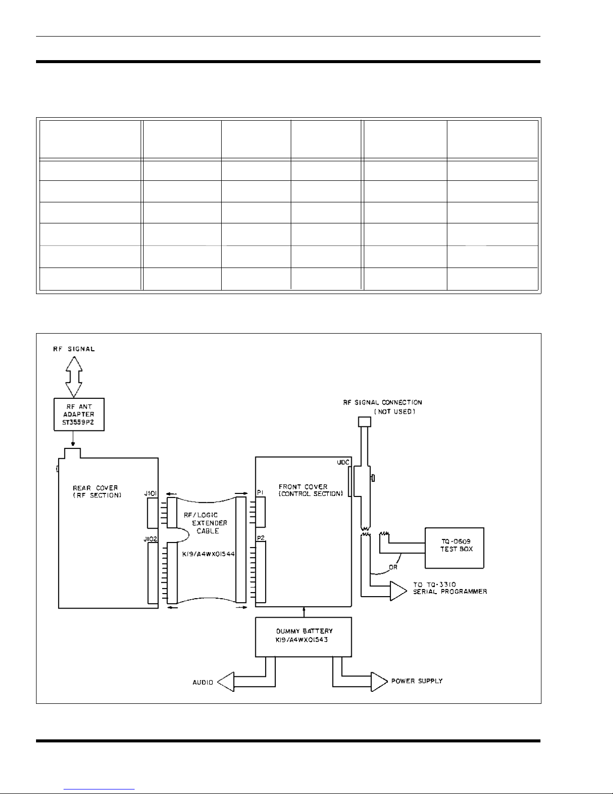
1. Separate the Front and Rear Cover Assemblies and con-
nect the RF/Logic Extender cable between the RF Board
and the Control Board. See Figure 6.
2. Slide the Dummy Battery onto the Front Cover Assem-
bly and connect the audio output leads to the distortion
analyzer. Place the Dummy Battery’s on/off switch in
the OFF position to direct the speaker audio to its speakers leads and to the distortion analyzer. Connect the PC
Programmer to the UDC.
3.
Set the power supply to 7.5 ±0.1 Vdc and connect the
Dummy Battery supply leads to the power supply.
4. Program the radio with the LO W, MIDDLE and HIGH-
side test channels listed in Table 2. To fully test the
transmitter, program a channel pair for each frequency,
one at high-power and one at low-power. It may be
desirable to program more test channels into the unit.
Figure 4 - Speaker, Microphone And Flex Circuit Access Figure 5 - Keypad Flex Access
6
LBI-38632
5. Remove power f rom the radio and r eplace t he PC pro-
gramming cable with the TQ-0609 Test Box.
6. Connect the radio to the wattmeter using the RF Antenna
Adapter. C o uple a small amount of the RF signal to the
frequency counter.
SERVICE NOTES
Throughout the service procedures presented in this
manual, the following information should be observed:
• The bench power supply s hould be set for 7.5
±0.1 Vdc (unless otherwise noted) during trou-
bleshooting procedures presented in this manual. If a battery pack is used, it should be fully
charged. Typical battery pack voltage will be
7.5 Vdc ±20% over its full discharge cycle.
• Logic Levels:
Logic 1 = high = greater than 4.5 Vdc
Logic 0 = low = less than 0.5 Vdc
• The modules are not field repairable. Schemat-
ics and outline diagrams for the modules are
presented in this manual as a troubleshooting
reference only.
• The Front Cover Test Accessory Kit allows the
Control Board to be extended out of the case for
troubleshooting access. The Keypad circuits
can be tested in the case via a PC computer
connection.
TRANSMITTER ALIGNMENT
The following infomation can be used to test and align
the transmitter’s output and its modulation characteristics.
Completion of these tests/alignments will verify a near 100%
operating synthesizer and transmitter stages.
Reference Oscillator
NOTE
Reference Oscillator U4 is factory adjusted and
should not normally n eed readjustment. U se a re-
cently calibrated and stable frequency counter t o
determine if oscillator alignment is needed. This
test/alignment should be done at a room tempera-
ture of 25°C ±5°C.
1. On the TQ-0609 Test Box, select UDC switch position
6 and apply power to the radio. This enables the radio’s
control circuits for an external microphone and its inter-
nal speaker amplifier.
2. Channel the unit to 860.5125 MHz (low-power) and key
the transmitter using the TQ-0609. DO NOT apply any
modulation at this time.
NOTE
• The personality information stored in the radio
should be backed-up on the PC computer before
any service procedure is performed.
Table 2 - RF Test Cha nn els
TEST FREQUENCY (MHz)
RF BAND LOW MIDDLE HIGH
806-824 MHz* 806.0125 815.5125 824.0000
851-869 MHz 851.0125 860.5125 869.0000
* Transmit only (RX channels are 45 MHz higher)
LBI-38203 contains detailed information on the
TQ-0609 Test Box.
3. Monitor the t ransmitter’s frequency an d adjust Refer-
ence Oscillator U4 to a frequency reading of 860.5125
MHz ±100 Hz (a small trimmer hole is located on top of
module). If the ±100 Hz maximum error (at room tem-
perature) cannot be secured, Reference Oscillator re-
placement may be necessary. Table 3 list maximum
transmitter errors for the specified temperature range.
4.
Check all TX test channels for an error of less than ±100
Hz.
7
LBI-38632
Table 3 - Maximum Tr an s mitter Fr equency Errors*
And Typical VCO (TP 2 ) TX Tu ning V olt ag es
CHANNEL TOLERANCE* LOWEST HIGHEST VCO TUNING BAND SWITCH
(MHz) (Hz) (MHz) (MHz) VOLTAGE (J102 pin 3)
806.012500 ±1209 806.011291 806.013709 1.5 Vdc low
815.512500 ±1223 815.511277 815.513723 2.9 Vdc low
824.000000 ±1236 823.998764 824.001236 4.2 Vdc low
851.012500 ±1277 851.011223 851.013777 1.9 Vdc high
860.512500 ±1291 860.511209 860.513791 3.1 Vdc high
869.000000 ±1304 868.998696 869.001304 4.2 Vdc high
* Based on specified ±1.5 ppm over the entire operating temperature range.
8
Figure 6 -Test Set-Up

LBI-38632
VCO Modulation
NOTE
VCO Modulation adjustment should only be necessary if changes in the Tracking Data values will not
compensate deviation levels to within specifications. Adjustment of R5 will obs olete all Tracking
and Channel Data modulation values. See the
"TRACKING AND CHANNEL DATA" section
in this manual for further details.
R5 "course aligns" the VCO modulation level. The
Audio Processor IC will perform "fin e le vel adj ustment" of TX deviation via the Tracking and Channel
Data.
1. To align R5 it will be necessary to modify the RF/Logic
Extender cable as follows:
• Add two 10K ohm resistors in series from 5.4 Vdc
(J102 pin 6) to ground (J102 pin 7).
• Break the connection at TX AUDIO, J102/P2 pin 1.
• Bias TX AUDIO into the RF Board to 2.7 Vdc by
connecting the junction of the 10K resistors to J102
pin 1.
Distortion Test
Measure transmitter audio distortion on the LOW, MIDDLE and HIGH-side test channels. Distortion readings
should be less than 3% at ±3 kHz deviation with a 1000 Hz
tone.
RECEIVER ALIGNMENT
The following information can be used to check and
align the receiver circuits. Successful completion of these
alignment procedures will verify a near 100% operating
synthesizer and receiver stages.
NOTE
There are no front-end filter, mixer or high-IF ad-
justments.
2nd Local Oscillator
1. Check the Reference Oscillator alignment a s outlined in
the "TRANSMITTER ALIGNMENT " section.
2. Channel the unit to 860.5125 MHz.
2.
Using a 100 µF (or greater) capacitor, couple a 1 kHz,
600 mV rms audio signal into TX AUDIO, J102 pin 1.
3. C onnect the radio to the modulation analyzer and key
the transmitter at 815.5125 MHz.
4.
Adjust the R5 for a deviation of ±4.3 kHz ±100 Hz.
Unkey the radio.
5. C heck low-frequency modulation as follows:
• Remove the 1 kHz signal and apply a 20 Hz, 1
Vp-p square wave. NOTE: The modulation
analyzer should have a low-frequency response
of less than 1 Hz for this test.
• Key the transmitter and monitor the demodu-
lated output from the modulation analyzer.
Check for a good square wave response at
860.5125 MHz. If the modulation peaks are not
flat, slightly readjust R5 for a good demodulated square wave. If this readjustment causes
the 1 kHz modulation set in step 4 to go outside
of the specified window, U4 may need to be
replaced.
3. Set the RF signal generator to 860.5125 MHz, -20 dBm
and no modulation. Apply this signal to the radio.
4. To measure the IF signal, connect the frequency counter
to TP1 on the RF Board or to the collector of Q1 on
Back-End Module U14. Use an appropriate high imped-
ance probe (or amp).
5. Adjust the signal generator level to achieve accurate
counting of the IF signal; the RF signal generator should
be set 10 dBm above the lowest level which gives
accurate counting.
6. Adjust the 2nd local oscillator via L13 for 455.000 kHz
±90 Hz.
Quadrature Detector
1.
Modulate the signal generator with a 1 kHz tone, ±3 kHz
deviation at 860.5125 MHz. Set the RF level to -50 dBm.
2. Adjust L14 for maximum audio level at J101/P1 pin 4.
9

LBI-38632
12 dB SINAD and Distortion Tests
1. Connect the distortion analyzer or SINAD meter to the
speaker load (in Dummy Battery).
2. With the RF signal generator and radio set to 860.5125
MHz, modulate the generator with a 1 kHz tone at ±3
kHz deviation. Measure the 12 dB SINAD sensitivity.
This reading should be equal to or better than -116 dBm
(0.35 µ V).
3. Return the signal level to -50 dBm.
4. Check audio distortion. Readings should be less than 5%
at rated audio output. Audio amplitude should be 100 150 mV rms (≈350 mVp-p) at J101/P1 pin 4.
5. Repeat the 12 dB SINAD sensitivity and distortion
check for the LOW and HIGH-side test channels. See
Table 2.
TRACKING AND CHANNEL DATA
The personality memory in the radio includes distinct
areas which are reserved for Tracking and Channel Data.
Tracking Data establishes individual radio parameters
and tailors the operation of the unit across the band. The
parameters are: high RF power, low RF power, mo dulation
level and receiver squelch opening. This data is programmed
into the RAM (U1) on the Control Board at the factory after
the front and rear covers are "married". The PC Programmer
allows alteration of this data if necessary.
Channel Data is the individual channel information such
as TX and RX frequencies, CG information, CCT information, and the four previously mentioned parameters. This
data is stored in the RAM on a per channel basis as each
channel is programmed. The PC Programmer allows alteration of this data (on a per channel basis) if necessar y .
Low, middle and high-side of the band values are programmed into the radio for each T racking parameter per band
(806-825 and 851-870). When a channel is added to the
radio, the Programmer reads the T racking Data stored in the
radio and calculates necessary values for each parameter
using a linear interpolation technique. The Programmer then
stores the newly calculated values in the Channel Data area
of memory along with the associated channel information.
Changing the Tracking Data in the radio will not alter Channel Data of previously programmed channels.
Tracking Data should not norma lly be altered; however,
it may be necessary to reprogram some of the values after
aligning circuitry, or replacing modules or other components
which obsolete the previously programmed values. Settings
for each parameter are listed in Table 4. If Tracking Data is
altered for the above reason, it will be necessary to reprogram
all channels to establish the new default data for each channel. See the Programming Manual for further information on
altering Tracking and Channel Data.
Digital values stored for the POWER SET analog voltage are one example of t racking information. As no two
transmitter stages are exactly matched, the POWER SET dc
voltage will be slightly different with any two radios to
produce the same power output. Tracking and Channe l Data
allows the microprocessor to tailor the POWER SET line for
RF stage gain differences from unit-to-unit and across the
band.
Table 4 - Tracking Data Parameters
PARAMETER FACTORY SETTINGHEX VALUE*
High-P o w er 3 .0 W a tts 85
Low-Po w er 1.0 Watt 50
Modulation ±4.3 kHz ** 0A
Squelc h Op e ni ng 8 dB SINAD A0
* Listed hex values are approximate; final pro-
grammed values will vary from unit-to-unit and
will need to be adjusted as such.
** EXT MIC HI = 1 kHz, 110 mV rms
TROUBLESHOOTING
The following procedures are designed to quickly lead
the service technician to the area of trouble. Rear and Front
Cover Assembly troubleshooting procedures are outlined.
Also see LBI-38834 for t roublshooting procedures that apply to later Front Cover Assembly 19D903620G1 (less Control Board).
The test set-up should be identical to the set-up used in
the "ALIGNMENT PROCEDURES" section in this manual. T able 5 lists common problems and most likely problem
areas.
REAR COVER ASSEMBLY
The troubleshooting procedures that follow primarily
assume a problem has been narrowed to a problem on the RF
Board. Transmitter, receiver and synthesizer symptoms/causes are outlined.
10

Transmitter Troubleshooting
Inoperative Or Low Power
Power sources and regulated power s upplies should be
one of the first areas to check before troubleshooting any
transmitter problem. The radio’s power source, whether it is
a battery or a bench power supply, is especially critical when
troubleshooting a portable radio. Current consumption is an
excellent troubleshooting tip when troubleshooting a dead or
weak transmitter. See Table 6 for complete radio current
consumption data.
If the synthesizer does not lock or stay locked at the start
of or during a transmission, I/O Microcontroller will not
enable or continue the transmission and the radio will beep
intermittantly or continously. Check LOCK detect at
J102/P2 pin 8 for a low or pulsi ng (not locked) condition.
See "
Synthesizer Troubleshooting" for further details.
1. C heck for batter y power on J102/P2 pin 2.
SERVIC E NOTES
Throughout the service procedures presented in this
manual, the following information should be ob-
served:
LBI-38632
2.
Check for 5.4 Vdc ±0.1 Vdc at J102/P2 pin 6 with the
transmitter enabled. Also check the operation of the TX
5.4V switch to insure 5.4 Vdc is being delivered to the
RF Board at J101/P1 pin 5 when the PTT button is
pressed.
3. Battery power should be present at the Power Amplifier
module pins 3 and 4. If current consumption appears
normal for both high and low-power modes, the probl em
may be Antenna T/R Switch module U2, the Low-pass
Filter module U5 or antenna switch SW1. If the Lowpass Filter module or the antenna switch have a problem,
generally the receiver will also be weak. A defective pin
diode inside the Antenna T/R Switch module m ay cause
transmitter and/or receiver problems.
4. I f low R F power i s a symptom, check the o peration of
Power Controller A2 and Q4. POWER SET on J101/P1
pin 1 should be approximately 1.8 Vdc in low-power
mode and 2.9 Vdc in high-power mode. If Q4 is saturated (collector voltage is approximately 7.5 Vdc), troubleshoot the PA U1 and Exciter U9 for a gain problem.
Also check the VCO and Q6 for low RF drive. Buffer
Q6 supplies approximately 0 dBm to U9. Exciter U9 has
an approximate gain of 23 dB and P A U1 has an approximate gain of 16 dB.
5. Check T racking a nd Channel Data. Reprogram if neces-
sary.
Excessive Power Output
• The bench power supply should be set for 7.5
±0.1 Vdc (unless otherwise noted) during trou-
bleshooting procedures presented in this manual. If a battery pack is used, it should be fully
charged. Typical battery pack voltage will be
7.5 Vdc ±20% over its full discharge cycle.
• Logic Levels:
Logic 1 = high = greater than 4.5 Vdc
Logic 0 = low = less than 0.5 Vdc
• The modules are not field repairable. Schemat-
ics and outline diagrams for the modules are
presented in this manual as a troubleshooting
reference only.
• The Front Cover T est Accessory Kit allows the
Control Board to be extended out of the case
for troubleshooting access. The Keypad circuits can be tested in the case via a PC computer
connection.
• The personality information stored in the radio
should be backed-up on the PC computer before any service procedure is performed.
Short battery life and possible damage to the PA module
may result if this problem occurs in the power controlling
circuitry.
1. C heck POWER SET from the Control Board. POWER
SET on J101/P1 pin 1 should be approximately 1.8 Vdc
in low-power (1 Watt) mode and 2.9 Vdc in high-power
(3 Watts) mode. If incorrect, troubleshoot the D/A con-
verter circuits (in Audio Processor U7) on the Control
Board. Check Tracking and Channel Data. Reprogram
if necessary.
2. The collector of Q4 should be approximately 3.5 Vdc in
low-power mode and 5.5 Vdc in high-power mode. If
Q4’s collector stays near 7.5 Vdc in receive mode, it is
most likely shorted. Temporarily short the emitter and
base while monitoring the collect or voltage. If t he col-
lector voltage falls, there is a problem in Power Control-
ler A2.
11

LBI-38632
Table 5 - General Troubleshooting
SYMPTOM POSSIBLE CAUSES
Completely inoperative (no audio 1. Dead Battery Pack.
and no LCD indication) 2. Fuse blown: Check radio fuse in Battery Plate.
3. Control Board problem.
At power-up, radio beeps:
a. twice (once in addition to 1a. Weak Battery P ack.
power-up beep)
b. continuously at an 1b. Unit is not programmed: Program ra dio - See TQ - 3364.
≈2 Hz rate 2b. Lithium battery on Control Board defective.
3b. Synthesizer is not locked: Check LOCK detect line, synthesizer
loading and VCO tun ing vo ltag e.
4b. RAM failure on Control Board.
5b. Interprocessor communication failure on Control Board.
Receiver inoperative or weak 1. Squelch levels programmed too high: Press Monitor Button to
disable squelch.
2. Channel Guard or T y p e 99 E nabled: See Operator’s M a nual.
3. Defective antenna.
4. RF Board problem: Troubleshoot Rear Cover Assembly.
Transmitter inoperative or low 1. Power levels programmed l ow: Check RF out put a nd r ep r og ram
range unit if necessary.
2. Weak battery.
3. Defective antenna.
4. RF Board problem: Troubleshoot Rear Cover Assembly.
TX and RX inoperative on some 1. Programming incorrect: Reprogram unit - See TQ-3364.
channels only 2. Synthesizer problem (VCO or prescaler):
Check LOCK de te c t (h igh = lo ck), VCO tuning voltag e a nd
modulas control line.
3. RAM problem: Troubleshoot Control Board.
TX and RX inoperative on all 1. Programming incorrect: Reprogram unit - See TQ-3364.
channels2. Synthesizer problem: Check LO CK dete ct (high = lock), VCO
tuning voltage and modulas control line.
3. Control Board problem.
4. Check SW1, U2 and U5 o n RF Board.
Trunk Mode Problems 1. Modem circuitry problem: Check U5, U6.1 and U17.3 and associated
circuitry on Control Board.
2. Low-speed data problem: T rouble sh oot the r elated e n code or
decode circuitry on Control Board.
Frequency Error
Modulation Problems
If transmit frequency error exists (greater than 1.5 ppm)
when the synthesizer is locked, Reference Oscillator U4
alignment or replacement is necessary . See " ALIGNMENT
PROCEDURES" for details. The I/O Microcontroller will
not enable a transmission if the synthesizer is not locked.
12
Modulation problems can be caused by a failures in the
audio circuits in the front cover or the modulating circuitry
of the RF Board.

LBI-38632
1. Verify modulating audio is present on J102/P2 pin 1. A
1 kHz, 600 mV rms TX AUDIO signal at this point
should produce approximately ±5.0 kHz deviation. Im-
proper modulation from 300 - 3000 Hz points to a VCO
modulation problem. Check the VCO pin 2 for the TX
AUDIO signal. Suspect the VCO if the signal is present
and incorrect modulation exists.
2. I f improper l ow-frequency modulation exists (Channel
Guard and trunked mode low-speed data), first check
J102 pin 1 for the proper tone. Next check U4 pin 3 for
the tone; suspect C11 if the tone is not present. Replace
U4 if the tone is present on pin 3 and incorrect low-frequency modulation exists. See the "ALIGNMENT
PROCEDURES" for details.
3. Check T racking a nd Channel Data. Reprogram if neces-
sary.
4. See the troubleshooting information in the "FRONT
COVER AS SEMBLY" section relating to the Control
Board.
Distorted Modulation
Check TX AUDIO for an u ndistorted signal to the RF
Board. The audio signal on J102/P2 pin 1 should appear
undistorted at maximum deviation and it should be riding on
a 2.7 Vdc bias developed on the Control Board.
1. If TX AUDIO distortion is minimal and transmitter
distortion is excess ive, suspect the VCO or the Reference Oscillator on the RF Board.
2. C heck RX AUDIO on J1 01/P1 pin 4 f or signal and/or
noise. With an RF input modulated at 1 kHz, ±3 kHz
deviation, RX AUDIO should be 100 - 150 mV rms
(approximately 350 mV p-p). If the 1 kHz audio is
present, troubleshoot the audio circuits in the Front
Cover Assembly. Noise levels on RX AUDIO with no
RF input should be approximately 700 mV p-p.
3. C heck for 7.5 Vdc at RF Amp U10 pin 5 and IF Amp
U11 pin 1. Check U14 pin 7 for 5.8 Vdc (±0.2 Vdc) from
A1 pin 10. Verify TX 5.4V is low in receive mode.
4. Verify mixer injection through Q2 from the VCO is
present at TP7. Check the VCO output with a frequency
counter at TP7. The VCO should be running 45.0125
MHz below the RX frequency. VCO output power level
is typically +4 dBm at TP7 into 50 ohms (mixer impedance).
5. To test the back-end circuits, follow this procedure:
• Verify 5.8 Vdc (±0.2 Vdc) is present on U14
pins 1 and 7.
• Connect a frequency counter to TP1 to monitor
the IF. Use a high-impedance probe (or amp).
• Couple a 45.0125 MHz signal (no modulation)
from an HF signal generator to TP4. Adjust the
signal generator level to achieve accurate
counting of the IF; the signal generator should
be set 10 dBm above the lowest level which
provides stable counting of the 455 kHz I F. See
the "ALIGNMENT PROCEDURES" sec tion
if the 2nd IF is in error by more than 90 Hz.
2. I f TX AUDIO is distorted, su spect a defective microphone, mic amps, modulation limiting, or pre-emphasis
circuity.
If audio sensitivity is good, the microphone, amplifiers
and limiters are p robably OK. Regeneration from an open
decoupling capacitor may make the unit appear to be too
sensitive. See the troubleshooting information in the
"FRONT COVER ASSEMBLY" section relating to the
Control Board.
Receiver Troubleshooting
Inoperative
1. If the synthesizer is not locked the radio should be
beeping and flashing "NO LOCK" in the LCD. See
"
Synthesizer Troubleshooting".
• Modulate the HF signal generator and observe
the recovered audio on U14 pin 2 and J101 pin
4.
Low Sensitivity
Low receiver sensitivity and/or failure of a modulation
acceptance bandwidth test indicates a receiver gain or selectivity problem in the IF stages. An excessively wide bandwidth will cause unnecessary noise, detracting from the
receiver quieting. If the bandwidth is too narrow squelching
could occur at the modulation peaks. Suspect a defective IF
filter if one of the above symptoms occurs.
A 12 dB SINAD sensitivity of around -90 dBm indicates
a problem with H igh-IF Amp U 11. The module provides a
nominal gain of around 17 dB.
A 12 dB SINAD sensitivity of around -100 dBm could
be caused by a problem with RF Amp U10. This module
provides 10 dB of gain.
13

LBI-38632
Squelch Problem
A squelch circuit problem (assuming good signal and/or
noise is present at J101 pin 4) indicates a problem with the
Audio Processor chip on the Control Board. Troubleshooting
should begin at the discriminator output. Signal trace
through the discriminator amp to the Audio Processor. Check
the operation of the noise rectifier to verify the noise is being
converted into the proper dc voltage. See the troubleshooting
information in the "FRONT COVER ASSEMBLY" section
relating to the Control Board.
Excessive Distortion
If the measu red distortion exceed s the rated specification signal trace starting at the discriminator output and
through the audio stages until the fault i s isolated. Signal
tracing with an oscilloscope proves very useful in locating
the trouble areas.
Synthesizer Troubleshooting
Will Not Loc k O r S tay Lock ed
Each time the channel is changed, the PTT Button is
pressed or the PTT Button is released, Synthesizer IC U3 is
serially loaded with new TX or RX d ata. If the synthesizer
does not lock or stay locked, the following will be observed:
• the radio continuously or intermittently beeps
• LOCK detect (J102 pin 8) will be low or puls-
ing to flag the I/O Microcontroller of the unlocked condition
If this condition occurs, the I/O Microcontroller will
continue to try to reload U3 with channel data until the
synthesizer locks.
4. Using a frequency counter with a high impedance probe
or amp, check TP8 for the 13.2 MHz (±20 Hz at room
temperature) signal from Reference Oscillator U4. Replace U4 if this signal is not present and pin 1 is 5.4 Vdc.
Also verify the signal is present on U3 pin 2. See
"ALIGNMENT PROCEDURES" for oscillator align-
ment details.
5. Verify BAND SWITCH (J102 pin 3) is at the correct
logic level. It should be low for transmit frequencies of
806 - 825 MHz and high for transmit frequencies of 851
- 870 MHz. BAND SWITCH should remain low for all
receive frequencies. (The VCO operates 45.0125 MHz
below the 851 - 870 MHz receive frequencies.) Suspect
the I/O Microcontroller on the Control Board if there is
a problem with the BAND SWITCH line. Check Y3 pin
5 for an inversion of this logic level via Q5. If the correct
inverted level is present on both bands and the synthesizer will not lock on one band onl y , re pla ce the VCO.
6. If LOCK detect is low and not pulsing, temporarily pull
it high by connecting J102 pin 6 to J102 pin 8. I f the
radio now operates normally on all test TX and RX
channels, replace U3 - the output on pin 9 is defective.
7. Check the VCO output with a frequency count er at T P7
or by tuning a service monitor to the radio’s local osc illator (VCO) signal and loosely couplin g the VCO signal
into the service monitor. The VCO should be running
45.0125 MHz below the RX frequency. VCO output
power level is typically +4 dBm at TP7 into 50 o hms
(mixer impedance). VCO tuning voltage can be monitored at TP2 or the VCO pin 1. See Table 3 for details.
8. I f a synthesizer lock p roblem cannot be narrowed to a
problem in the Rear Cover Assembly, reprogram the
inoperative channels and test the unit again. Also see the
service information on the Control Board for further
details.
Excessive Switching Time
1.
V erify the 5.4 Vdc supply to the RF Board is within ±0.1
Vdc, 7.5V B ATT is present, and TX 5.4 V is low (receive
mode only).
2. Monitor CLOCK, DATA and ENABLE (on J102 pins
11, 10 and 9 respectively) for pulse activity when the
channel is changed. See Figure 8 for specific waveform
details. If these signals are not present, suspect a defec-
tive I/O Microcontroller on the Control Board.
3.
Check A1 pin 9 for 5.8 Vdc (±0.2 Vdc) to U3, U4, U8
and the VCO. If this power source is not present, check
A1 pin 7 f or 5.8 Vdc (±0.2 Vdc) from Q201 and check
A1 pin 11 for 7.5 Vdc. Replace A1 if the inputs are good
and the output is not.
14
The synthesizer should generally lock within 10 milli-
seconds after a frequency change.
1. Su spect leaky low-pass filter capacitors C57 or C58 if
slow switching time is a symptom. Replace these components with original equipment parts only. See the RF
Board parts list for part numbers.
2. Module A1 also influences switching time. Verify the
ENABLE pulse is present at A1 pin 4. See Figure 8.
 Loading...