

Ericsson 19D902797G8, 19D902797G7, 19D902797G9, 19D902797G6, 19D902797G10 Maintenance Manual
...
LBI-38674E
TABLE OF CONTENTS
DESCRIPTION . . . . . . . . . . . . . . . . . . . . . . . . . . . . . . . . . . . . . . . . . . . . . . . 1
SPECIFICATIONS . . . . . . . . . . . . . . . . . . . . . . . . . . . . . . . . . . . . . . . . . . . . . 1
CIRCUIT ANALYSIS . . . . . . . . . . . . . . . . . . . . . . . . . . . . . . . . . . . . . . . . . . . . 1
POWER AMPLIFIER . . . . . . . . . . . . . . . . . . . . . . . . . . . . . . . . . . . . . . . . . 1
Exciter . . . . . . . . . . . . . . . . . . . . . . . . . . . . . . . . . . . . . . . . . . . . . . . 1
Small Signal Gain Stage . . . . . . . . . . . . . . . . . . . . . . . . . . . . . . . . . . . . . . 1
Low Level Amplifier . . . . . . . . . . . . . . . . . . . . . . . . . . . . . . . . . . . . . . . . 1
Driver . . . . . . . . . . . . . . . . . . . . . . . . . . . . . . . . . . . . . . . . . . . . . . . . 1
Power Amplifier Finals . . . . . . . . . . . . . . . . . . . . . . . . . . . . . . . . . . . . . . 1
POWER CONTROL . . . . . . . . . . . . . . . . . . . . . . . . . . . . . . . . . . . . . . . . . . . . . 2
Theory of Operation . . . . . . . . . . . . . . . . . . . . . . . . . . . . . . . . . . . . . . . . 2
Signal Interface . . . . . . . . . . . . . . . . . . . . . . . . . . . . . . . . . . . . . . . . . . . 2
TROUBLESHOOTING GUIDE . . . . . . . . . . . . . . . . . . . . . . . . . . . . . . . . . . . . . . 2,3
BLOCK DIAGRAM . . . . . . . . . . . . . . . . . . . . . . . . . . . . . . . . . . . . . . . . . . . . . 1
POWER AMPLIFIER READINGS . . . . . . . . . . . . . . . . . . . . . . . . . . . . . . . . . . . . . 3
ASSEMBLY DIAGRAM . . . . . . . . . . . . . . . . . . . . . . . . . . . . . . . . . . . . . . . . . . 5,6,7
PARTS LIST . . . . . . . . . . . . . . . . . . . . . . . . . . . . . . . . . . . . . . . . . . . . . . . . . 8
PRODUCTION CHANGES . . . . . . . . . . . . . . . . . . . . . . . . . . . . . . . . . . . . . . . . 10
IC DATA . . . . . . . . . . . . . . . . . . . . . . . . . . . . . . . . . . . . . . . . . . . . . . . . . . . 11
OUTLINE DIAGRAM . . . . . . . . . . . . . . . . . . . . . . . . . . . . . . . . . . . . . . . . . . . 10,12
SCHEMATIC DIAGRAM . . . . . . . . . . . . . . . . . . . . . . . . . . . . . . . . . . . . . . . . . 11,12
LOW PASS FILTER . . . . . . . . . . . . . . . . . . . . . . . . . . . . . . . . . . . . . . . . . . . . . 7,13
MAINTENANCE MANUAL FOR
450-470 MHz, 110 WATT POWER AMPLIFIER
19D902797G3
425-450 MHz, 90 WA TT POWER AMPLIFIER
19D902797G7
403-425 MHz, 90 WA TT POWER AMPLIFIER
19D902797G6
380-400 MHz, 75 WA TT POWER AMPLIFIER
19D902797G8
470-494 MHz, 90 WA TT POWER AMPLIFIER
19D902797G9
492-512 MHz, 90 WA TT POWER AMPLIFIER
19D902797G10
410-430 MHz, 90 WA TT POWER AMPLIFIER
19D902797G11
ericssonz
Ericsson Inc.
Private Radio Systems
Mountain View Road
Lynchburg, Vi rginia 24502
1-800-528-7711 (Outside USA, 804-528-7711) Printed in U.S.A.
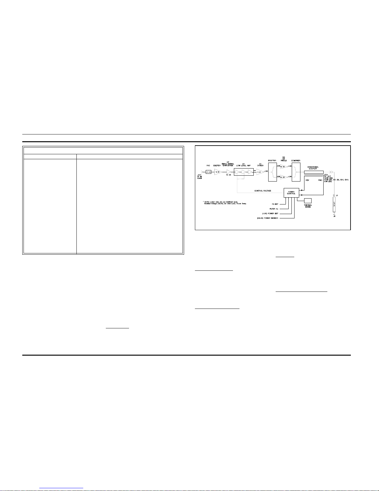
DESCRIPTION
The UHF Power Amplifier Assembly is a wide band RF
power amplifier operating over the 380-400, 410-430, 403425, 425-450, 450-470, 47 0-494, and 492-512 MHz range
without tuning. Its main function is to amplify the 10 mW FM
signal from the Transmitter Synthesizer to the rated RF output
at the antenna port. The output of the Power Amplifier Assembly is adjustable from rated power to 3dB lower at the P A output
J104.
The assembly consists of a printed wiring board (A1) and
associated components, including a power module and three
RF power transistors, mounted to the heat sink assembly. The
printed wiring board (A1) contains both the power amplifier
circuitry and the power control circuitry.
Unfiltered supply voltage, A+, for the power amplifier
circuits enters the assembly via feedthrough capacitor, C1.
Power cable W4 routes the A+ from C1 to J103 on the PWB.
Filtered A+ voltage for the power control circuit enters the
assembly via control cable W13 which connects to the PWB at
J201.
The Power Control circuitry sets the output power level by
adjusting the PA Power Set level. It keeps the output power
constant despite variations in input power, power amplifier
gain, or temperature through the use of a feedback control loop
in the PA assembly.
CIRCUIT ANALYSIS
POWER AMPLIFIER
The power amplifier section of the PA Board consists of
an Exciter, a Small Signal Gain Stage, a Low Level Amplifier,
a Driver, and the Power Amplifier Finals. All these gain sta ges
have an input and output impedance of 50 ohms. Figure 1 is a
block diagram showing the signal flow within the Power Amplifier Assembly.
Exciter (U101)
The Exciter stage uses a broadband silicon monolithic
microwave integrated circuit (MMIC) amplifier. The signal
from transmitter synthesizer, typically 10 dBm (10 mW), is
input to the Exciter through a 10 dB resistive pad (R1, R2, and
R31). The Exciter amplifies the resulting 0 dBm (1 mW)
signal to 12 dBm (16 mW).
The MMIC requires a 5 volt supply sour ce. The 8 volt
regulator (U100) provides the 5 volts to the MMIC via a
dropping resistor R30.
Small Signal Gain Stage
The Small Signal Gain Stage consists of Q7 and its
associated bias and matching circuitry. Collector voltage is
fed through R39, R40, and L23. Resistor R33 sets the quiescent bias of the part. The transistor input impedance is
matched to the 50 ohm output of the Exciter by C59, C61,
C62, and C63. L24 provides the nece s sar y out put mat c hing.
The stage provides 14 dB of gain to amplify the signal from
the Exciter to 26 dBm (400 mW).
Low Level Amplifier (U102)
The Low Level Amplifier (LLA) stage uses a 50 ohm
thick film RF Power Module to amplify and control of the
output power. Internally, the module is a three stage amplifier. The power control circuitry controls the gain of the first
and second stages by varying the collector voltage level of
Q203. The third stage gain remains constant with A+ providing the DC supply voltage.
The signal from the Small Signal Gain stage, typically
26 dBm (400 mW), is input into the LLA. Under typical
Power Set conditions, the LLA amplifies the signal to a
typical output level of 40.5 dBm (11.2 W).
Driver (Q1)
The driver is a 6 dB RF amplifier consisting of transistor
Q1 and its associated circuitry. The signal from the LLA,
typically 40.5 dBm (11.2 W), is amplified to 46.5 dBm (45.0
W). The transistor input is matched to 50 ohms by C65, C66,
C27, C67, and a piece of pr inted tran smissio n line. Th e drive
signal is then split with a printed in-phase Wilkenson splitter,
providing equal power to each of the final devices.
Power Amplifier Finals (Q2, Q3)
Each of the Power Amplifier Final devices is capable of
producing 5 to 6 dB of gain. The output signal from the
Splitter is impedance matched to each of the finals. Under
optimum conditions each final amplifies the input signal to
between 50 and 70 watts output power (depending on band
split). The outputs are then impedance matched to the input
of the Combiner. The Combiner is a printed in-phase Wilkinson type which combines (sums) the output power of the
finals. This produces an output power of approximately
100W, (depending on band split) which is coupled to the
directional coupler (part of A1 PWB) and on to the antenna
circuits. In addition, the directional coupler samples both
forward and reverse power and sends this sample to the
Power Control circuitry.
Copyright © July 1992, Ericsson GE Mobile Communications Inc.
Table 1 - General Specifications
ITEM SPECIFICATION
FREQUENCY 450 MHz - 470 MHz (G3)
403 MHz - 425 MHz (G6)
425 MHz - 450 MHz (G7)
380 MHz - 400 MHz (G8)
470 MHz - 494 MHz (G9)
492 MHz - 512 MHz (G10)
410 MHz - 430 MHz (G11)
OUTPUT POWER (RF) 65 watts - 130 watts (G3)
55 watts - 110 watts (G6, G7, G9, G10 & G11)
45 watts - 90 watts (G8)
INPUT POWER (RF) 10 mW min. into ≤ 2:1 VSWR.
TEMPERATURE RANGE -30°C TO +60°C (Ambient air)
SUPPLY VOLTAGE 13.4 Vdc
CURRENT 29 Amps max. (26 A typical @ rated power, 13.4V) (G3)
29 Amps max. (21 A typical @rated power , 13.4V)(G6, G7, G9, G10 & G11)
29 Amps max. (20 A typical @ rated power, 13.4V) (G8)
DUTY CYCLE Continuous
STABILITY Stable into 3:1 VSWR; all temp.,voltage,freq. 55 watts - 110 watts (G3)
or 45 watts - 90 watts (G6, G7, G9, G10 & G11) or 45watts - 90 watts (G8)
RUGGEDNESS AT HIGH VSWR No damage into open or shorted load.
Figure 1 - Block Diagram
LBI-38674
1

POWER CONTROL
The Power Control circuitry performs three basic functions. It keys and unkeys the PA, sets the PA output power,
and protects the PA against adverse conditions.
Keying and Unkeying the PA
To key the PA, the digital controller places 5 volts on
the PA key line, J201-2. Zero volts on the PA key line causes
the PA to unkey. If the control cable (W13) is disconnected,
with nothing actively driving the PA key line, the PA will
remain unkeyed.
PA Output Power Set
PA output power is set according to the level of the
Power Set line. Four (4) volts on this line will produce
minimum power. As the voltage increases toward eight (8)
volts, the power will increase to its maximum rated output.
The PA output power is initially set at the factory. This is
done by adjusting R43 while injecting a 10 mW signal at J1
and applying 8 volts to J201-3. After setting the maximum
power level, changing the output power in done by varying
the voltage applied on the Power Set line.
PA Protection
The power control also protects the PA against over
temperature and high VSWR conditions.
An over temperature condition exists when the flange
temperature of the final output transistor reaches 80°C. At
this point the output power will drop below its set level. The
output power will continue to drop such that when the flange
temperature reaches 12 5°C the PA output drops at least 10
dB below its set level.
Reflected power is limited to 25% of the set power. If
the output VSWR degrades to worse than 3:1 the forward
power will be reduced to limit the reflected power to 25% of
the set power. The Power Sensor line indicates when the PA
is operating in a cutback condition. If the PA is keyed and
the power control is cutting back, the Power Sensor line will
drop to zero (0) volts and the PA alarm light on the station
will turn on.
Theory of Operation
Power control of the MASTR III Power Amplifier is
accomplished with a feedback control loop. The three possible feedback signals are: representation of forward power,
temperature sensitive scaled representat ion of forward
power, or representation of reflected power. These three
signals are input to a diode summing junction which selects
the largest of the three for use as the feedback.
The stripline directional coupler samples the output
power and produces a voltage, Vf, propor tional to the forward output power. The power control comp ares the forward
voltage, Vf, to a reference voltage at U3. The output of U3
controls the current flow thru Q5 and the output of Q203.
The collector output of Q203 adjusts the control voltage,
Vct1 and Vct2. This control voltage is capable of adjusting
the total PA output power since it provides the fir st two stages
DC supply to the Low Level Amplifier, U1.
During over temperat ure operation, a scaled representation of the forward power is maintained constant by
varying the control voltage line. Thermal resistor RT1 sensing an increase in temperature causes the output of U3.1 to
increase. If the output of U3.1 becomes larger than the other
feedback lines, the output of U3.4 will begin to decrease.
This in turn will cause the output of Q203 to decrease
reducing the supply voltage to U1. Since the scaling is a
function of temperature the power is reduced as the temperature increases.
Under VSWR cutback operation the reverse voltage, Vr,
representative of the reflected output power is held below a
threshold by reducing the cont rol volt age a s ne ce ss ary. If Vr
increases at U3.1 bey o nd the preset threshold an increase at
U3.4 will result. This causes a subsequent reduction in the
control voltage to U1. Thus the power control circuit reduces
the output power in order to limit the reflected power to 25%
of the set power.
Signal Interface
The signal interface to the MASTR III Power Amplifier
is supported by a six position feedthrough connector, J201,
with the following pinout:
1
– PWR Sensor
2
– PA Key
3
– PA PWR Set
4
– NC
5
– Ground
6
– Fil A+
Pwr Sensor
This line indicates when the PA is expe riencing adverse
conditions. Under normal operation, while the PA is keyed,
this line will be proportional to forward power. Minimum
power (zero watts) corresponds to 2.5 volts while maximum
power corresponds to 4.5 volts. This voltage is not temperature compensated and no effort is made to calibrate this
signal to an absolute power level. It is intended to provide a
relative indication of forward power and to discriminate
between normal and cutback operation.
Zero volts on this line, when the PA is keyed, indicates the
forward power is cutback. This power cutback may be due to
high reflected power or may be due to high PA temperatures.
This fault condition may indicate a problem with the PA or may
indicate a system problem external to the Power Amplifier.
High VSWR may be due to a poor antenn a an d hig h tempe rature may be due to a blocked cabinet vent. Zero volts on this
line, when the PA is keyed, does not indicate zero forward
power. Zero volts indicates the PA is protecting itself due to
adverse conditions. If the adverse condition, either high VSWR
or high temperature is eliminated, the power will return to
normal and the PWR SENSOR voltage will rise above 2.5
volts.
PA Key (Interface Connector pin 2)
This line is used to key and unkey the PA. UNKEY = 0
volt and KEY = 5 volts. The driver of this line must be capable
of supplying 5 volts at 1.0 mA. The appropriate key sequence
requires RF from the transmit synthesizer be input to the PA
before the KEY line is energized.
PA PWR Set (Interface Connector pin 3)
This line is used to set the RF Power Output of the PA.
Minimum power output equals 4 volts and maximum power
output equals 8 volts. The driver of this line must be capable
of supplying 8 volts at 1.0 mA.
Fil A+ (Interface Connector pin 6)
This line provides the filtered supply voltage for the Power
Control. The driver of this line must be capable of supplying
13.4 volts ±20% at 100 mA.
SYMPTOM AREAS TO CHECK INDICATIONS
1. No Power or low Power at 1. Measure the transmitter output The presence of power at this port
Antenna Port. p ower before the duplexer or is an indication of a defective
antenna switch (for simplex mode). duplexer, switch, or cables.
2. Measure the transmitter output The presence of power at this port
power before the low pass filter. is an indication of a defective filter
or cables.
3. Measure the transmitter output The presene of power at this port
power before the optional isolator is an indication of a defective isolator
at the PA output port. or cables.
2. No power at PA output port 1. Station is in receive mode.
and PA ALARM is OFF.
3. No power at PA output port 1. No RF input to PA. Check TX Synthesizer should deliver
and PA ALARM is ON. connection between PA and TX a minimum of 10 mW
Synthesizer. (10 dBm) to the PA.
2. Check the logic or DC inputs to
the PA from the Interface Board
through J201.
a. J201-2 PA KEY 5volts during transmit
b. J201-3 POWER SET 4 volts to 8 volts (4 volts
represents zero RF power)
c. J201-6 13.8 VF 13.8 Vdc ±20%
3. Defective PA Replace PA
TROUBLESHOOTING GUIDE
LBI-38674
2
SYMPTOM AREAS TO CHECK INDICATIONS
4. Low power at PA output port 1. Low RF input to PA from TX Power should be a minimum of 10
and PA ALRAM is OFF. Synthesizer. mW (10 dBm).
2. Check the voltage on J201-3 For minimal output power, this
(POWER SET). voltage should be above 7 volts.
3. Check the power supply voltage Voltage should be minimal 13.4
on the collector of Q1, Q2 Vdc.
and Q3
4. One of the two final PA Replace the defective transistor.
transistors (Q2 or Q3) is
defective.
5. Low power at PA output port 1. Check for over temperature and/ The power control circuit protects
and PA ALARM is ON. or a high VSWR condition due to the PA by cutting back the power.
a mismatch at the output port. In case of a mismatch, refer to
symptom 1.
TROUBLESHOOTING GUIDE (cont’d)
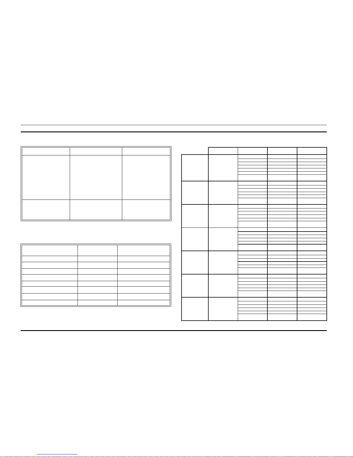
PARAMETER REFERENCE READINGS
(50 ohm, -30°C to +60°C) SYMBOL (volts DC)
SUPPLY VOLTAGE A+ 13.4 V ±20%
CONTROL VOLTAGE Vct1 0 - 12 V
FORWARD VOLTAGE Vf 3 - 7 V
REVERSE VOLTAGE Vr 2 - 6 V
POWER SENSE J201-1 2.5 - 4 V
PA KEY J201-2 5 V
POWER SET J201-3 4 - 8 V
13.8 VF J201-6 13.8 V ±20%
UHF POWER AMPLIFIER VOLTAGE CHART
Group Low Mid High
Frequency G3
G6
G7
G8
G9
G10
G11
450 MHZ
403 MHZ
425 MHZ
380 MHZ
470 MHZ
492 MHZ
410 MHZ
460 MHZ
414 MHZ
437 MHZ
390 MHZ
482 MHZ
502 MHZ
420 MHZ
470 MHZ
425 MHZ
450 MHZ
400 MHZ
494 MHZ
512 MHZ
430 MHZ
Vct 1 (Volts DC) G3
G6
G7
G8
G9 & G10
G11
7 - 10 Volts
6 - 8 Volts
6 - 8 Volts
6 - 8 Volts
6 - 8 Volts
6 - 8 Volts
6 - 8 Volts
6 - 8 Volts
6 - 8 Volts
6 - 8 Volts
6 - 8 Volts
6 - 8 Volts
4 - 6 Volts
6 - 8 Volts
6 - 8 Volts
6 - 8 Volts
6 - 8 Volts
6 - 8 Volts
Vf (Volts DC) G3
G6
G7
G8
G9 & G10
G11
5 - 7 Volts
6 - 8 Volts
6 - 8 Volts
6 - 8 Volts
6 - 8 Volts
6 - 8 Volts
5 - 7 Volts
6 - 8 Volts
6 - 8 Volts
6 - 8 Volts
6 - 8 Volts
6 - 8 Volts
5 - 7 Volts
6 - 8 Volts
6 - 8 Volts
6 - 8 Volts
6 - 8 Volts
6 - 8 Volts
Vr (Volts DC) G3
G6
G7
G8
G9 & G10
G11
2 - 3 Volts
2 - 3 Volts
2 - 3 Volts
2 - 3 Volts
2 - 3 Volts
2 - 3 Volts
2 - 3 Volts
2 - 3 Volts
2 - 3 Volts
2 - 3 Volts
2 - 3 Volts
2 - 3 Volts
2 - 3 Volts
2 - 3 Volts
2 - 3 Volts
2 - 3 Volts
2 - 3 Volts
2 - 3 Volts
J201 - 1 (Volts DC) G3
G6
G7
G8
G9 & G10
G11
2.5 - 4 Volts
2.5 - 4 Volts
2.5 - 4 Volts
2.5 - 4 Volts
2.5 - 4 Volts
2.5 - 4 Volts
2.5 - 4 Volts
2.5 - 4 Volts
2.5 - 4 Volts
2.5 - 4 Volts
2.5 - 4 Volts
2.5 - 4 Volts
2.5 - 4 Volts
2.5 - 4 Volts
2.5 - 4 Volts
2.5 - 4 Volts
2.5 - 4 Volts
2.5 - 4 Volts
J201 - 3 (Volts DC) G3
G6
G7
G8
G9 & G10
G11
6 - 8 Volts
6 - 8 Volts
6 - 8 Volts
6 - 8 Volts
6 - 8 Volts
6 - 8 Volts
6 - 8 Volts
6 - 8 Volts
6 - 8 Volts
6 - 8 Volts
6 - 8 Volts
6 - 8 Volts
6 - 8 Volts
6 - 8 Volts
6 - 8 Volts
6 - 8 Volts
6 - 8 Volts
6 - 8 Volts
J201- 6 (Volts DC) G3
G6
G7
G8
G9 & G10
G11
13.4 Volts
13.4 Volts
13.4 Volts
13.4 Volts
13.4 Volts
13.4 Volts
13.4 Volts
13.4 Volts
13.4 Volts
13.4 Volts
13.4 Volts
13.4 Volts
13.4 Volts
13.4 Volts
13.4 Volts
13.4 Volts
13.4 Volts
13.4 Volts
UHF POWER AMPLIFIER TYPICAL VOLTAGE READINGS
(50 ohm, room temperature, 13.4 Vdc supply voltage, and rated output)
LBI-38674
3

FREQUENCY STANDARD ADJUSTABLE WITH WITH WITH DUPLEXER
MHz @J2 RANGE DUPLEXER ISOLATOR AND ISOLATOR
@J104
450-470 110W 65-130W 75W 100W 70W
425-450 90W 55-110W 60W 82W 55W
403-425 90W 55-110W 60W 82W 55W
380-400 75W 45-90W 50W 68W 47W
410-430 90W 55-110W 60W 82W 55W
470-494 90W 55-110W 60W 82W 55W
492-512 90W 55-110W 60W 82W 55W
RATED POWER FOR MASTR III UHF BASE STATION
LBI-38674
4
 Loading...