

Page 1
LBI-38674C
Printed in U.S.A.
TABLE OF CONTENTS
DESCRIPTION . . . . . . . . . . . . . . . . . . . . . . . . . . . . . . . . . . . . . . . . . . . Front Cover
SPECIFICATIONS . . . . . . . . . . . . . . . . . . . . . . . . . . . . . . . . . . . . . . . . . 1
CIRCUIT ANALYSIS . . . . . . . . . . . . . . . . . . . . . . . . . . . . . . . . . . . . . . . . 1
POWER AMPLIFIER . . . . . . . . . . . . . . . . . . . . . . . . . . . . . . . . . . . . . 1
Exciter . . . . . . . . . . . . . . . . . . . . . . . . . . . . . . . . . . . . . . . . . . . 1
Small Signal Gain Stage . . . . . . . . . . . . . . . . . . . . . . . . . . . . . . . . . . 1
Low Level Amplifier . . . . . . . . . . . . . . . . . . . . . . . . . . . . . . . . . . . . 1
Driver . . . . . . . . . . . . . . . . . . . . . . . . . . . . . . . . . . . . . . . . . . . . 1
Power Amplifier Finals . . . . . . . . . . . . . . . . . . . . . . . . . . . . . . . . . . 1
POWER CONTROL . . . . . . . . . . . . . . . . . . . . . . . . . . . . . . . . . . . . . . . . . 1
Theory of Operation . . . . . . . . . . . . . . . . . . . . . . . . . . . . . . . . . . . . 2
Signal Interface . . . . . . . . . . . . . . . . . . . . . . . . . . . . . . . . . . . . . . . 2
TROUBLESHOOTING GUIDE . . . . . . . . . . . . . . . . . . . . . . . . . . . . . . . . . . 3
BLOCK DIAGRAM . . . . . . . . . . . . . . . . . . . . . . . . . . . . . . . . . . . . . . . . . 1
POWER AMPLFIER READINGS . . . . . . . . . . . . . . . . . . . . . . . . . . . . . . . . . 3
ASSEMBLY DIAGRAM . . . . . . . . . . . . . . . . . . . . . . . . . . . . . . . . . . . . . . 4
PARTS LIST . . . . . . . . . . . . . . . . . . . . . . . . . . . . . . . . . . . . . . . . . . . . . 6
IC DATA . . . . . . . . . . . . . . . . . . . . . . . . . . . . . . . . . . . . . . . . . . . . . . . 11
OUTLINE DIAGRAM . . . . . . . . . . . . . . . . . . . . . . . . . . . . . . . . . . . . . . . 8
ASSEMBLY DIAGRAM . . . . . . . . . . . . . . . . . . . . . . . . . . . . . . . . . . . . . . 8
SCHEMATIC DIAGRAM . . . . . . . . . . . . . . . . . . . . . . . . . . . . . . . . . . . . . . 9
LOW PASS FILTER . . . . . . . . . . . . . . . . . . . . . . . . . . . . . . . . . . . . . . . . . 8
MAINTENANCE MANUAL FOR
450-470 MHz, 110 WATT POWER AMPLIFIE R
19D902797G3
425-450 MHz, 90 WAT T POWER AMPLIFIER
19D902797G7
403-425 MHz, 90 WAT T POWER AMPLIFIER
19D902797G6
DESCRIPTION
The UHF Power Amplifier Assembly is a wide band RF
power amplifier operating over the 403-425, 425-45 0 and
450-470 MHz range without tuning. Its main function is to
amplify the 10 mW FM signal from the Transmitter Synthesizer to the rated RF output at the antenna port. The output
of the Power Amplifier Assembly is adjustable from rated
power to 3dB lower at the PA output J104.
The assembly consists of a printed wiring board (A1)
and associated componen ts, includ ing a power modu le and
three RF power transistors, mounted to the heat sink assembly. The printed wiring board (A1) contains both the power
amplifier circuitry and the power control circuitry.
Unfiltered supply voltage, A+, for the power amplifier
circuits enters the assembly via feedthrough capacitor, C1.
Power cable W4 routes the A+ from C1 to J103 on the PWB.
Filtered A+ voltage for the power control circuit enters the
assembly via control cable W13 which connects to the PWB
at J201.
Page 2
The Power Control circuitry sets the output power level by
adjusting the PA Power Set level. It keeps the output power
constant despite variations in input power, power amplifier
gain, or temperature through the use of a feedback control loop
in the PA assembly.
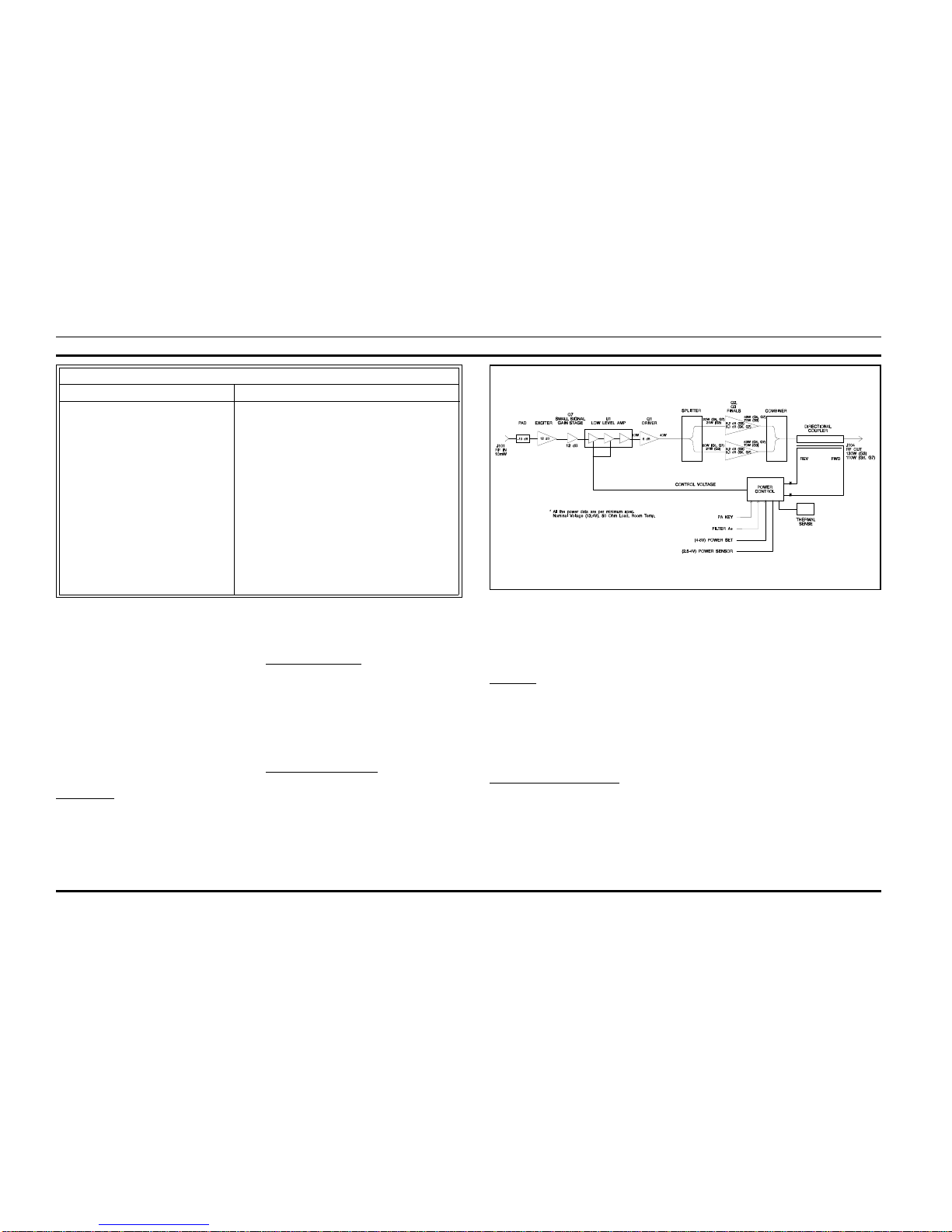
CIRCUIT ANALYSIS
POWER AMPLIFIER
The power amplifier section of the PA B oard consists of
an Exciter, a Small Signal Gain Stage, a Low Level Amplifier,
a Driver, and the Power Amplifier Finals. All these gain stages
have an input and output impedance of 50 ohms. Figure 1 is a
block diagram showing the signal flow within the Power Amplifier Assembly.
Exciter (U101)
The Exciter stage uses a broadband silicon monolithic
microwave integrated circuit (MMIC) amplifier. The signal
from transmitter synthesizer, typically 10 dBm (10 mW), is
input to the Exciter throug h a 10 dB re s ist i v e pad (R 1, R 2, a nd
R31). The Exciter amplifies the resulting 0 dBm (1 mW) signal
to 12 dBm (16 mW).
The MMIC requires a 5 volt supply source. The 8 volt
regulator (U100) provides the 5 volts to the MMIC via a
dropping resistor R30.
Small Signal Gain Stage
The Small Signal Gain Stage consists of Q7 and its associated bias and matching circuitry. Collector voltage is fed
through R39, R40, and L23. Resistor R33 sets the quiescent
bias of the part. The transistor input impedance is matched to
the 50 ohm output of the Exciter by C59, C61, C62, and C63.
L24 provides the necessary output matching. The stage provides 14 dB of gain to amplify the signal from the Exciter to
26 dBm (400 mW).
Low Level Amplifier (U102)
The Low Level Amplifier (LLA) sta ge uses a 50 ohm thick
film RF Power Module to amplify and control of the output
power. Internally, the module is a three stage amplifier. The
power control circuitry controls the gain of the first and second
stages by varying the collector voltage level of Q203. The third
stage gain remains constant with A+ providing the DC supply
voltage.
The signal from the Small Signal Gain stage, typically
26 dBm (400 mW), is input into the LLA. Under typical
Power Set conditions, the LLA amplifies the signal to a
typical output level of 40.5 dBm (11.2 W).
Driver (Q1)
The driver is a 6 dB RF amplifier consisting of transistor
Q1 and its associated circuitry. The signal from the LLA,
typically 40.5 dBm (11.2 W), is amplified to 46.5 dBm (45.0
W). The transistor input is matched to 50 ohms by C65, C66,
C27, C67, and a piece of printed transmission line. The drive
signal is then split with a printed in-phase Wilkenson splitter,
providing equal power to each of the final devices.
Power Amplifier Finals (Q2, Q3)
Each of the Power Amplifier Final devices is capable of
producing 5.2 (G3) [5.0 ( G6, G7)] dB of gain. The output
signal from the Splitter is impedance matched to each of the
finals. Under optimum conditions each final amplifies the
43.3 dBm (21 W) (G3) [43.0 d Bm (2 0W) (G6, G7)] power
input signal to 48.45 dBm (70 W) (G3) [48.0 dBm (63W)
(G6, G7)] output power. The outputs are then impedance
matched to the input of the Combiner. The Combiner is a
printed in-phase Wilkinson type which combines (sums) the
output power of the finals. This produces an output power of
approximately 51.1 dBm (130 W) (G3) [50.5 dBm (110W)
(G6, G7)] which is coupled to the directional coupler (part
of A1 PWB) and on to the antenna circuits. In addition, the
directional coupler samples both forward and reverse power
and sends this sample to the Power Control circuitry.
POWER CONTROL
The Power Control circuitry pe rforms three basic functions. It keys and unkeys the PA, sets the PA output power,
and protects the PA against adverse conditions.
Keying and Unkeying the PA
To key the P A, the digital controller places 5 vo lts on the
PA key line, J201-2. Zero volts on the PA key line causes the
PA to unkey . If the control cable (W13) is disconnected, with
nothing actively driving the PA key line, the PA will remain
unkeyed.
PA Output Power Set
PA output power is set according to the level of the
Power Set line. Four (4) volts on this line will produce
minimum power. As the voltage increases toward eight (8)
Copyright © July 1992, Ericsson GE Mobile Communications Inc.
Table 1 - General Specifications
ITEM SPECIFICATION
FREQUENCY 450 MHz - 470 MHz (G3)
403 MHz - 425 MHz (G6)
425 MHz - 450 MHz (G7)
OUTPUT POWER (RF) 65 watts - 130 watts (G3)
55 watts - 110 watts (G6, G7)
INPUT POWER (RF) 10 mW min. into ≤ 2:1 VSWR.
TEMPERATURE RANGE -30°C TO +60°C (Ambient air)
SUPPLY VOLTAGE 13.4 Vdc
CURRENT 29 Amps max. (26 A typical @ 130W, 13.4V) (G3)
29 Amps max. (21 A typical @ 110W, 13.4V) (G6, G7)
DUTY CYCLE Continuous
STABILITY Stable into 3:1 VSWR; all temp.,voltage,freq. 65
watts - 130 watts (G3) or 55 watts - 110 watts (G6, G7)
RUGGEDNESS AT HIGH VSWR No damage into open or shorted load.
Figure 1 - Block Diagram
LBI-38674
1
Page 3

volts, the power will increase to its maximum rated output.
The PA output power is initially set for an output of 130 watts
(G3), 110 watts (G6, G7) at J104. This is done by adjusting
R43 while injecting a 10 mW signal at J1 and applying 8
volts to J201-3. After setting the maximum power level,
changing the output power in done by varying the voltage
applied on the Power Set line.
PA Protection
The power control also protects the PA against over
temperature and high VSWR conditions.
An over temperature condition exists when the flange
temperature of the final output transistor reaches 80°C. At
this point the output power will drop below its set level. The
output power will continue to drop such that when the flange
temperature reaches 125°C the PA output drops at least 10
dB below its set level.
Reflected power is limited to 25% of the set power. If
the output VSWR degrades to worse than 3:1 the forward
power will be reduced to limit the reflected power to 25% of
the set power. The Power Sensor line indicates when the PA
is operating in a cutback condition. If the PA is keyed and
the power control is cutting back, the Power Sensor line will
drop to zero (0) volts and the PA alarm light on the station
will turn on.
Theory of Operation
Power control of the MASTR III Power Amplifier is
accomplished with a feedback control loop. The three possible feedback signals a re: representat ion of forward p ower,
temperature sensitive scaled representati on of forward
power, or representation of reflected power. These three
signals are input to a diode summing junction which selects
the largest of the three for use as the feedback.
The stripline directional coupler samples the output
power and produces a voltage, Vf, pro portional to the forward output power. Th e power con trol compares the f orward
voltage, Vf, to a reference voltage at U3. The output of U3
controls the current flow thru Q5 and the output of Q203.
The collector output of Q203 adjusts the control voltage,
Vct1 and Vct2. This control voltage is capable of adjusting
the total PA output power since it provides the first two stages
DC supply to the Low Level Amplifier, U1.
During over temperature operation, a scaled representation of the forward power is maintained constant by
varying the control voltage line. Thermal resistor RT1 sensing an increase in temperature causes the output of U3.1 to
increase. If the output of U3.1 becomes larger than the other
feedback lines, the output of U3.4 will begin to decrease.
This in turn will cause the output of Q203 to decrease
reducing the supply voltage to U1. Since the scaling is a
function of temperature the power is reduced as the temperature increases.
Under VSWR cutback operation the reverse voltage, Vr,
representative of the reflected output power is held below a
threshold by reducing the control voltage as necessary. If Vr
increases at U3.1 beyond the preset threshold an increase at
U3.4 will result. This causes a subsequent reduction in the
control voltage to U1. Thus the power control circuit reduces
the output power in order to limit the reflected power to 25%
of the set power.
Signal Interface
The signal interface to the MASTR III Power Amplifier
is supported by a six position feedthrough connector, J201,
with the following pinout:
1
– PWR Sensor
2
– PA Key
3
– PA PWR Set
4
– NC
5
– Ground
6
– Fil A+
Pwr Sensor
This line indicates when the PA is experiencing adve rse
conditions. Under normal operation, while the PA is keyed,
this line will be proportional to forward power. Minimum
power (zero watts) corresponds to 2.5 volts while maximum
power corresponds to 4.5 volts. This voltage is not temperature compensated and no effort is made to calibrate this
signal to an absolute power level. It is intended to provide a
relative indication of forward power and to discriminate
between normal and cutback operation.
Zero volts on this line, when the PA is keyed, indicates
the forward power is cutback. This power cutback may be
due to high reflected power or may be due to high PA
temperatures. This fault condition may indicate a problem
with the PA or may indicate a system problem external to the
Power Amplifier. High VSWR may be due to a poor antenna
and high temperature may be due to a blocked cabinet vent.
Zero volts on this line, when the PA is keyed, does not
indicate zero forward power. Zero volts indicates the PA is
protecting itself due to adverse conditions. If the adverse
condition, either high VSWR or high temperature is eliminated, the power will return to normal and the PWR SENSOR voltage will rise above 2.5 volts.
PA Key (Interface Connector pin 2)
This line is used to key and unkey the PA. UNKEY = 0
volt and KEY = 5 volts. The driver of this line must be capable
of supplying 5 volts at 1.0 mA. The approp riat e key seq uenc e
requires RF from the transmit synthesizer be input to the PA
before the KEY line is energized.
PA PWR Set (Interface Connector pin 3)
This line is used to set the RF Power Output of the PA.
Minimum power output equals 4 volts and m aximum power
output equals 8 volts. The driver of this line must be capable
of supplying 8 volts at 1.0 mA.
Fil A+ (Interface Connector pin 6)
This line provides the filtered supply voltage for the Power
Control. The driver of this line must be capable of supplying
13.4 volts ±20% at 100 mA.
SYMPTOM AREAS TO CHECK INDICATIONS
1. No Power or low Power at 1. Measure the transmitter output The presence of power at this
Antenna Port. power before the duplexer or port is an indication of a
antenna switch (for simplex defective duplexer, switch, or
mode). cables.
2. Measure the transmitter output The presence of power at this
power before the low pass filter. port is an indication of a
defective filter or cables.
3. Measure the transmitter output The presene of power at this
power before the optional isolator port is an indication of a
at the PA output port. defective isolator or cables.
2. No power at PA output port 1. Station is in receive mode.
and PA ALARM is OFF.
3. No power at PA output port 1. No RF input to PA. Check TX Synthesizer should deliver
and PA ALARM is ON. connection between PA and TX a minimum of 10 mW
Synthesizer. (10 dBm) to the PA.
2. Check the logic or DC inputs to
the PA from the Interface Board
through J201.
a. J201-2 PA KEY 5volts during transmit
b. J201-3 POWER SET 4 volts to 8 volts (4 volts
represents zero RF power)
c. J201-6 13.8 VF 13.8 Vdc ±20%
3. Defective PA Replace PA
TROUBLESHOOTING GUIDE
LBI-38674
2
Page 4
SYMPTOM AREAS TO CHECK INDICATIONS
4. Low power at PA output port 1. Low RF input to PA from TX Power should be a minimum
and PA ALRAM is OFF. Synthesizer. of 10 mW (10 dBm) .
2. Check the voltage on J201-3 For nominal output power,
(POWER SET). this voltage should be above
7 volts.
3. Check the power supply voltage Voltage should be nominal
on the collector of Q1, Q2 13.4 Vdc.
and Q3
4. One of the two final PA Replace the defective
transistors (Q2 or Q3) is transistor.
defective.
5. Low power at PA output port 1. Check for over temperature and/ The power control circuit proand PA ALARM is ON. or a high VSWR condition due to tects the PA by cutting back
a mismatch at the output port. the power. In case of a mis-
match, refer to symptom 1.
TROUBLESHOOTING GUIDE (cont’d)
FREQUENCY ADJUSTABLE WITH WITH WITH DUPLEXER
MHz STANDARD RANGE DUPLEXER ISOLATOR AND ISOLATOR
450-470 110W 65-130W 75W 100W 70W
425-450 90W 55-110W 60W 82W 55W
403-425 90W 55-110W 60W 82W 55W
RATED POWER FOR MASTR III UHF BASE STATION
PARAMETER REFERENCE READINGS
(50 ohm, -30°C to +60°C) SYMBOL (volts DC)
SUPPLY VOLTAGE A+ 13.4 V ±20%
CONTROL VOLTAGE Vct1 0 - 12 V
FORWARD VOLTAGE Vf 3 - 7 V
REVERSE VOLTAGE Vr 2 - 6 V
POWER SENSE J201-1 2.5 - 4 V
PA KEY J201-2 5 V
POWER SET J201-3 4 - 8 V
13.8 VF J201-6 13.8 V ±20%
UHF POWER AMPLIFIER VOLTAGE CHART
Group Low Mid High
Frequency G3
G6
G7
450 MHZ
403 MHZ
425 MHZ
460 MHZ
414 MHZ
437 MHZ
470 MHZ
425 MHZ
450 MHZ
Vct 1 (Volts DC) G3
G6
G7
7 - 10 Volts
6 - 8 Volts
6 - 8 Volts
6 - 8 Volts
6 - 8 Volts
6 - 8 Volts
4 - 6 Volts
6 - 8 Volts
6 - 8 Volts
Vf (Volts DC) G3
G6
G7
5 - 7 Volts
6 - 8 Volts
6 - 8 Volts
5 - 7 Volts
6 - 8 Volts
6 - 8 Volts
5 - 7 Volts
6 - 8 Volts
6 - 8 Volts
Vr (Volts DC) G3
G6
G7
2 - 3 Volts
2 - 3 Volts
2 - 3 Volts
2 - 3 Volts
2 - 3 Volts
2 - 3 Volts
2 - 3 Volts
2 - 3 Volts
2 - 3 Volts
J201 - 1 (Volts DC) G3
G6
G7
2.5 - 4 Volts
2.5 - 4 Volts
25 - 4 Volts
2.5 - 4 Volts
2.5 - 4 Volts
25 - 4 Volts
2.5 - 4 Volts
2.5 - 4 Volts
25 - 4 Volts
J201 - 3 (Volts DC) G3
G6
G7
6 - 8 Volts
6 - 8 Volts
6 - 8 Volts
6 - 8 Volts
6 - 8 Volts
6 - 8 Volts
6 - 8 Volts
6 - 8 Volts
6 - 8 Volts
J201- 6 (Volts DC) G3
G6
G7
13.4 Volts
13.4 Volts
13.4 Volts
13.4 Volts
13.4 Volts
13.4 Volts
13.4 Volts
13.4 Volts
13.4 Volts
UHF POWER AMPLIFIER TYPICAL VOLTAGE READINGS
(50 ohm, room temperature, 13.4 Vdc supply voltage, and rated output )
LBI-38674
3
Page 5

ASSEMBLY DIAGRAM
POWER AMPLIFIER ASSEMBLY
19D902797G3, G6 & G7
(19D902797 Sh.3 Rev.3)
LBI-38674
4
Page 6

ASSEMBLY DIAGRAM
POWER AMPLIFIER ASSEMBLY
19D902797G3, G6 & G7
(19D902797 Sh.2 Rev.6)
COVER ASSEMBLY
19B801659G3
(19B801659, Sh. 2, Rev. 3)
LBI-38674
5
Page 7

110 WATT UHF POWER AMPLIFIER
19D902797G3
90 WATT UHF POWER AMPLFIER
19D902797G6 & G7
ISSUE 3
PARTS LIST
SYMBOL PART NUMBER DESCRIPTION
— — — — ASSEMBLIES — — —
A1 POWER AMPLIFIER BOARD
19D902794G3, G6, G7
— — — — CAPACITORS — — —
C1 19A702052P26 Ceramic: 0.1 µF ±10%, 50 VDCW,
C2 19A702061P63 Ceramic: 120 pF ±5%, 50 VDCW,
thru temp coef 0 ±30 PPM.
C9
C10 344A3126P38 Porcelain: 100 pF ±5%, 500 VDCW.
C11 19A702061P63 Ceramic: 120 pF ±5%, 50 VDCW,
temp coef 0 ±30 PPM.
C12 19A705108P40 Mica chip: 1000 pF, ±10%, 500 VDCW.
C13 344A3126P38 Porcelain: 100 pF ±5%, 500 VDCW.
thru
C16
C17 19A702052P26 Ceramic: 0.1 µF ±10%, 50 VDCW.
C18 19A705108P40 Mica chip: 1000 pF, ±10%, 500 VDCW.
C19 344A3126P38 Porcelain: 100 pF ±5%, 500 VDCW.
C20 19A705108P40 Mica chip: 1000 pF, ±10%, 500 VDCW.
and
C21
C22 19A702052P26 Ceramic: 0.1 µF ±10%, 50 VDCW.
and
C23
C24 19A702061P63 Ceramic: 120 pF ±5%, 50 VDCW,
temp coef 0 ±30 PPM.
C25 344A3126P38 Porcelain: 100 pF ±5%, 500 VDCW.
and
C26
C27 344A3126P15 Porcelain: 12 pF ±5%, 500 VDCW (G6).
thru
C29
C27 344A3126P13 Porcelain: 10 pF ±5%, 500 VDCW (G7).
C28 344A3126P11 Porcelain: 8.2 pF ±5%, 500 VDCW (G7).
and
C29
C30 344A3126P11 Porcelain: 8.2 pF ±5%, 500 VDCW (G3).
and
C31
C32 344A3126P1 Porcelain: 3.3 pF ±.25pF, 500 VDCW
and (G3).
C33
C34 344A3126P18 Porcelain: 15 pF ±5pF, 500 VDCW
and (G6, G7).
C35
C36 344A3126P5 Porcelain: 4.7 pF ±5%, 500 VDCW (G6).
C42 19A702052P26 Ceramic: 0.1 µF ±10%, 50 VDCW.
thru
C45
C50 19A702052P26 Ceramic: 0.1 µF ±10%, 50 VDCW.
C51 19A705205P7 Tantalum: 10 µF, 25 VDCW; sim to
Sprague 293D.
C53 19A705205P7 Tantalum: 10 µF, 25 VDCW; sim to
and Sprague 293D.
C54
C57 19A705205P7 Tantalum: 10 µF, 25 VDCW; sim to
Sprague 293D.
*
COMPONENTS, ADDED, DELETED OR CHANGED BY PRODUCTION CHANGES
SYMBOL PART NUMBER DESCRIPTION
C58 344A3126P11 Porcelain: 8.2 pF ±5%, 500 VDCW
(G3).
C58 344A3126P15 Porcelain: 12 pF ±5%, 500 VDCW
(G6, G7).
C59 19A702061P49 Ceramic: 56 pF ±5%, 50 VDCW, temp
coef 0 ±30 PPM.
C60 19A702061P65 Ceramic: 150 pF ±5%, 50 VDCW,
temp coef 0 ±30 PPM/°C.
C61 19A702061P17 Ceramic: 12 pF ±10 pF, 50 VDCW,
temp coef 0 ±30 PPM/°C.
C62 19A702061P5 Ceramic: 2.2 pF ±5%, 50 VDCW, temp
coef 0 ±20 PPM/°C.
C64 344A3126P38 Porcelain: 100 pF ±5%, 500 VDCW.
C65 344A3126P11 Porcelain: 8.2 pF ±5%, 500 VDCW (G3).
C66 19A700006P50 Mica/teflon: 39 pF ±2%, 100 VDCW (G7).
thru
C69
C66 19A700006P48 Mica/teflon: 33 pF ±2%, 100 VDCW (G3).
C66 19A700006P50 Mica/teflon: 39 pF ±2%, 100 VDCW
(G6, G7).
C67 19A700006P58 Mica/teflon: 47 pF ±2%, 100 VDCW(G6).
C67 19A700006P50 Mica/teflon: 39 pF ±2%, 100 VDCW (G7).
C68 19A700006P50 Mica/teflon: 39 pF ±2%, 100 VDCW
(G6, G7).
C67 19A700006P49 Mica/teflon: 36 pF ±2%, 100 VDCW (G3).
C68 19A700006P48 Mica/teflon: 33 pF ±2%, 100 VDCW (G3).
C69 19A700006P49 Mica/teflon: 36 pF ±2%, 100 VDCW (G3).
C69 19A700006P58 Mica/teflon: 47 pF ±2%, 100 VDCW(G6).
C69 19A700006P50 Mica/teflon: 39 pF ±2%, 100 VDCW (G7).
C70 19A702061P49 Ceramic: 56 pF ±5%, 50 VDCW, temp
coef 0 ±30 PPM.
C71 19A702061P63 Ceramic: 120 pF ±5%, 50 VDCW,
temp coef 0 ±30 PPM.
C72 19A702052P26 Ceramic: 0.1 µF ±10%, 50 VDCW.
and
C73
C75 19A702052P26 Ceramic: 0.1 µF ±10%, 50 VDCW.
thru
C77
C78 19A705205P7 Tantalum: 10 µF, 25 VDCW; sim to
and Sprague 293D.
C79
C81 344A3126P62 Porcelain: 1000 pF ±5%, 500 VDCW.
C82 19A705108P40 Mica chip: 1000 pF, ±10%, 500
and VDCW.
C83
C84 19A702061P89 Ceramic: 1500 pF ±5%, 50 VDCW,
temp coef 0 ±30 PPM/°C.
C85 19A705108P40 Mica chip: 1000 pF ±10%, 500 VDCW
and
C86
C87 19A700006P50 Mica/teflon: 39 pF ±2%, 100 VDCW (G3).
C87 19A700006P58 Mica/teflon: 47 pF ±2%, 100 VDCW
(G6, G7).
C87 19A700006P57 Mica/teflon: 43 pF ±2%, 100 VDCW (G7).
thru
C90
C88 19A700006P59 Mica/teflon: 51 pF ±2%, 100 VDCW (G6).
and
C89
C88 19A700006P50 Mica/teflon: 39 pF ±2%, 100 VDCW (G3).
thru
C90
C90 19A700006P58 Mica/teflon: 47 pF ±2%, 100 VDCW (G6).
SYMBOL PART NUMBER DESCRIPTION
C91 19A700006P48 Mica/teflon: 33 pF ±2%, 100 VDCW (G3).
thru
C94
C91 19A700006P58 Mica/teflon: 47 pF ±2%, 100 VDCW(G6).
C91 19A700006P49 Mica/teflon: 36 pF ±2%, 100 VDCW (G7).
C92 19A700006P50 Mica/teflon: 39 pF ±2%, 100 VDCW
and (G7).
C93
C92 19A700006P57 Mica/teflon: 43 pF ±2%, 100 VDCW(G6).
and
C93
C94 19A700006P49 Mica/teflon: 36 pF ±2%, 100 VDCW (G7).
C94 19A700006P58 Mica/teflon: 47 pF ±2%, 100 VDCW(G6).
— — — — — DIODES — — — —
D1 19A705377P4 Silicon: 140 mW; sim to HP HSMS-2802.
thru
D3
D4 19A700053P3 Silicon: 2 Diodes in Series, Common
thru Cathode; sim to MBAV70L.
D6
— — — — — JACKS— — — — —
J101 19A705512P1 Connector, RF SMB Series: sim to
AMP No. 221111-1.
J103 19A134263P1 Contact, electrical: sim to Selectro
229-1082-00-0-590.
J201 19A704852P32 Printed wire, two part: 6 contacts, sim
to Molex 22-29-2061.
— — — — INDUCTORS— — — —
L1 19C320617P10 Coil.
L2 19A701091G1 Coil (G6, G7).
L3 19C320617P10 Coil (G6, G7).
L4 19C320617P28 Coil.
L5 19A701091G1 Coil (G6, G7).
L6 19C320617P10 Coil (G6, G7).
L7 19A705470P3 Coil, Fixed: 15 nH; sim to Toko
380NB-15nM.
L8 19A705470P8 Coil, Fixed: 39 nH; sim to Toko
380NB-39nM.
L14 19C320617P17 Coil.
L15 19A700024P13 Coil, RF: 1.0 µH ±10%.
thru
L17
L18 19C320617P17 Coil.
L23 19A705470P8 Coil, Fixed: 39 nH; sim to Toko
380NB-39nM.
L24 19A705470P1 Coil, Fixed: 10 nH; sim to Toko
380NB-15nM.
L25 19A701091G1 Coil.
L29 19C320617P10 Coil.
and
L30
— — — TRANSISTORS — — —
Q4 19A700076P2 Silicon, NPN: sim to MMBT3904, low
and profile.
Q5
Q7 344A3058P1 Silicon, NPN: sim to NE 46134.
— — — — RESISTORS— — — —
R1 19B800607P270 Metal film: 27 ohms ±5%, 1/8 w.
and
R2
SYMBOL PART NUMBER DESCRIPTION
R3 19B801486P101 Metal film: 100 ohms ±5%, 1/8 w.
thru
R6
R7 19B800607P183 Metal film: 18K ohms ±5%, 1/8 w.
R8 19B800607P103 Metal film: 10K ohms ±5%, 1/8 w.
thru
R10
R11 19B800607P223 Metal film: 22K ohms ±5%, 1/8 w.
R12 19B800607P103 Metal film: 10K ohms ±5%, 1/8 w.
thru
R18
R19 19B800607P472 Metal film: 4.7K ohms ±5%, 1/8 w.
and
R20
R21 19B800607P102 Metal film: 1K ohms ±5%, 1/8 w.
thru
R23
R24 19B800607P103 Metal film: 10K ohms ±5%, 1/8 w.
thru
R26
R27 19B800607P822 Metal film: 8.2K ohms ±5%, 1/8 w.
R30 19B800607P750 Metal film: 75 ohms ±5%, 1/8 w.
R31 19B800607P330 Metal film: 33 ohms ±5%, 1/8 w.
R32 19A700050P17 Wirewound: 2.2 ohms ±10%, 2 w (G3).
R33 19B800607P153 Metal film: 1.5K ohms ±5%, 1/8 w.
R34 19B801486P100 Metal film: 10 ohms ±5%, 1/2 w.
R35 19A700050P17 Wirewound: 2.2 ohms ±10%, 2 w (G3).
R36 19B801486P101 Metal film: 100 ohms ±5%, 1/2 w.
R37 19B801486P331 Metal film: 330 ohms ±5%, 1/2 w.
R38 19B800607P223 Metal film: 22K ohms ±5%, 1/8 w.
R39 19B800607P100 Metal film: 10 ohms ±5%, 1/8 w.
and
R40
R41 19A702931P333 Metal film: 21.5K ohms ±1%, 200
VDCW, 1/8 w.
R42 19A702931P293 Metal film: 9090 ohms ±1%, 200
VDCW, 1/8 w.
R43 19A700109P5 Variable: 25 ohms to 10K ohms ±20%,
1/4 w.
R44 19B801486P101 Metal film: 100 ohms ±5%, 1/2 w.
thru
R46
R47 19B801486P750 Metal film: 75 ohms ±5%, 1/2 w.
and
R48
R49 19B801486P101 Metal film: 100 ohms ±5%, 1/2 w.
R51 19B801486P331 Metal film: 330 ohms ±5%, 1/2 w.
R52 19B801486P101 Metal film: 10 ohms ±5%, 1/2 w.
— — — — THERMISTOR — — —
RT1 19A705813P2 Thermistor: sim to
AL03006-58.2K-97-G100.
— — INTEGRATED CIRCUITS —
U3 19A701789P4 Linear: Quad Op Amp; sim to LM224D.
U7 344A3907P1 Monolithic microwave IC (MMIC): sim
to Avantek MSA-1105.
— — VOLTAGE REGULATORS —
VR1 19A700083P102 Silicon: 5.1 Volt Zener; sim to
and BZX84-C5V1.
VR2
LBI-38674
6
Page 8

PARTS LIST
LOW PASS FILTER MODULE
19D902856G3
ISSUE 1
SYMBOL PART NUMBER DESCRIPTION
— — — — CAPACITORS — — —
C1 19A116708P2 Ceramic feedthru: 0.01 µF -0 +100%,
500 VDCW; sim to Erie
327-050-X5W0103P.
— — — — — JACKS — — — —
J1 Part of W1.
J104 7777145P5 Receptacle: sim to Amphenol 82-97.
— — — — TRANSISTORS — — —
Q1 344A3948P1 Silicon, NPN: UHF Amplifier; sim to
Motorola MRF 650.
Q2 344A4134P1 Silicon, NPN: UHF Amplifier.
and
Q3
Q203 19A700055P1 Silicon, PNP: Darlington; sim to
TIP-125.
— — — — RESISTORS — — —
R28 19A143832P6 Power: 100 ohm 5%, 40 w.
and
R29
— — INTEGRATED CIRCUITS —
U1 19A705457P2 PA module (G3).
U1 19A705457P1 PA module (G7).
U1 19a705457P4 PA module (G6).
U100 19A705532P2 Integrated Circuit, Linear (Positive
Voltage Regulator): sim to MC78T15CT.
— — — — — CABLES — — — —
W1 19B801529G4 RF Input Cable. Includes the following:
19B800560P2 RF Cable.
19A705512P3 Connector, RF SMB series: sim to AMP
228213-1.
19A115938P1 Connector, coaxial: (BNC Series); sim to
Amphenol 31-318.
W4 19B801695G11 Power Cable. Includes the following:
19B209268P115 Solderless terminal.
19B209260P11 Solderless terminal.
19A115959P2 Wire, stranded.
19A701503P2 Cable: battery, red.
19A701503P10 Cable: battery, black.
19B209268P116 Solderless terminal.
W10 19B801937P1 Power cable.
W13 19B801739P1 Power control cable.
— — — MISCELLANEOUS — —
2 19D902420P6 Heatsink.
5 19A702381P510 Screw, thread forming: TORX DRIVE
No. M3.5 0.6 x 10.
6 7139898P3 Nut, hex, brass: No. 1/4-28.
11 19A702364P310 Machine screw, TORX Drive: No.
M3-0.5 x 10.
16 19A700136P7 Insulated sleeving.
20 19B235310P1 Nameplate.
21 19A701863P27 Clip, loop.
22 19A701312P5 Flatwasher: M3.5.
28 19A702364P316 Machine Screw: Pan Head, Steel.
29 19A700034P4 Nut, hex: No. M3 x 0.5MM.
30 19A700033P5 Lock washer, external tooth: No. 3.
35 19A705469P1 Insulator Plate, TO-220.
36 19A700068P1 Insulator, bushing.
SYMBOL PART NUMBER DESCRIPTION
— — — — — JACKS — — — —
J1 7777145P5 Receptacle: sim to Amphenol 82-97.
and
J2
— — — MISCELLANEOUS — —
2 19D903063P1 Casting.
3 19D903064P1 Casting.
4 19D902853G3 UHF Filter Board. See separate parts
list.
5 19A702381P513 Screw, thread forming: TORX, No.
M3.5 - 0.6 X 13.
6 19A702364P210 Machine screw, metric: M2.5-.45 x 10.
7 19A134455P3 Flatwasher.
8 19A700032P3 Lockwasher, tooth, steel, metric: 2.5.
10 19B235310P1 Nameplate.
UHF FILTER BOARD
19D902853G3
— — — — CAPACITORS — — —
C1 19A700006P2 Mica: 5.6 pF ±10%, 100 VDCW; sim to
thru Underwood 3HS0020.
C3
C4 19A700006P1 Mica: 4.7 pF ±10%, 100VDCW.
C5 19A700006P2 Mica: 5.6 pF ±10%, 100 VDCW; sim to
Underwood 3HS0020.
— — — — INDUCTORS — — —
L1 19C320618P7 Coil.
and
L2
L3 19B227929P1 Coil.
thru
L6
— — — MISCELLANEOUS — —
11 19A702455P5 Nut, self clinching.
*
COMPONENTS, ADDED, DELETED OR CHANGED BY PRODUCTION CHANGES
PRODUCTION CHANGES
Changes in the equipment to improve performance or to simplify
circuits are identified by a "Revisio n Letter" which is stamped after
the model number of the unit. The revision stamped on the unit
includes all previous revisions. Refer to the Parts List for the
descriptions of parts af fe ct ed by th ese re vis ion s.
PRODUCTION CHANGES
REV. A
POWER AMPLIFIER 19D902797G3
POWER AMPLIFIER BOARD 19D902794G3
To make unit ETS compliant.
C17, C44, C45 were 19A702 05 2P33 .
C50 was 0.068 µF (19A702052P24).
C61 was 8.2 pF (19A702061 P12) .
C62 was 27 pF (19A702061P3 3).
C84 was 1000 pF (19A705108 P4 0).
D1, D2, D3 were (19A700047P3)
L15 thru L17 were (19A7000 24P3 7).
L24 was 15nH (19A705470P3).
R33 was 5.6K (19B800607P5 62).
R34 was 3.9 ohms composition (19A700113P5).
L26 and L27 were removed.
C48, C49, C63, C74 were removed.
C1, (19A702052P26) was added.
C25, C26 (344A3126P38) were added.
R37, R51 (19B801486P331) were added.
R52 (19B801486P100) was adde d.
Q7 was 19A701940P1.
RT1 (19A705813P2) was added.
VR2 (19A700083P102) was adde d.
REV. B
POWER AMPLIFIER 19D902797G3
POWER AMPLIFIER BOARD 19D902794G3
To update PWB for new split.
PWB changed
C26 was 100 pF (344A3126P38).
C81 was 100 pF (344A3126P38).
C27 thru C29 added: 8.2 pF (3 44 A312 6P11 ).
C34 and C35 added: 12 pF (344 A312 6P 15).
R36 was 150 ohms (19B801486P151).
R44 thru R46 were 150 ohm (19B801486P151).
R47 and R48 were 39 ohm (19B80 14 86P3 90 ).
R32 and R35 added: 2.2 ohm (19A700050P17).
SYMBOL PART NUMBER DESCRIPTION
37 19A134455P3 Flat washer.
38 19B801659G3 Cover (see separate parts list).
41 19A700033P6 Loackwasher, external tooth, M3.5.
45 N405P5B6 Lockwasher.
46 19A701312P4 Flatwasher: 3.2 ID.
50 19A702381P408 Tap screw, TORX Drive, M3-0.5 x 8.
51 19A705106P1 Resistor Spacer.
COVER
19B801659G3
2 19D902421P1 Power Amplifier Cover.
4 19A702381P522 Screw, thread forming:
5 19A701365P4 Washer.
11 19A149969P3 Shield.
13 5493477P9 Axial fan.
14 5493477P10 Grille.
15 N80P13028B6 Machine screw.
16 N210P21B6 Machine nut.
17 19A701312P5 Flatwasher: M3.5.
18 19A701863P10 Clip, loop.
20 19A702364P410 Machine screw.
24 N405P37B6 Lock washer.
25 L401P23B6 Split washer.
26 19A700034P5 Hex nut.
LBI-38674
7
Page 9

OUTLINE AND ASSEMBLY DIAGRAMS
POWER AMPLIFIER BOARD A1
19D902856G3, G6 & G7
(19D902794, Sh. 2, Rev. 2)
COMPONENT SIDE
LOW PASS FILTER MODULE
19D902856G3
(19D902856 Sh.1 Rev.0)
LBI-38674
8
Page 10

SCHEMATIC DIAGRAM
POWER AMPLIFIER ASSEMBLY
19D902797G3, G6 & G7
(19D903622 Sh.1 Rev.6)
LBI-38674
9
Page 11

OUTLINE AND SCHEMATIC DIAGRAMS
LOW PASS FILTER MODULE
19D902856G3
(19D903623 Sh.1 Rev. 1)
(19D902853, Sh. 2, Rev. 0)
(19D903638, Component Side, Rev. 0)
COMPONENT SIDE
(19D902853, Sh. 2, Rev. 0)
(19D903638, Solder Side, Rev. 0)
SOLDER SIDE
POWER AMPLIFIER ASSEMBLY
19D902797G3, G6 & G7
(19D903622 Sh.2 Rev. 6)
LBI-38674
10
Page 12

IC DATA
U1
19A705457P1, P2 AND P4
PA Amplifier Module
U3
19A701789P4
Quad Op-Amp
U100
19A705532P2
Voltage Regulator
U7
344A3907P1
MMIC Amplifier
LBI-38674
11
 Loading...