

Page 1
Printed in U.S.A.
TABLE OF CONTENTS
Page
DESCRIPTION . . . . . . . . . . . . . . . . . . . . . . . . . . . . . . . . . . . . . . . . . . . Front Cover
CIRCUIT ANALYSIS . . . . . . . . . . . . . . . . . . . . . . . . . . . . . . . . . . . . . . . . Front Cover, 1
PARTS LIST . . . . . . . . . . . . . . . . . . . . . . . . . . . . . . . . . . . . . . . . . . . . . 5
OUTLINE DIAGRAM . . . . . . . . . . . . . . . . . . . . . . . . . . . . . . . . . . . . . . . . 6
INTEGRATED CIRCUITS . . . . . . . . . . . . . . . . . . . . . . . . . . . . . . . . . . . . . 7
SCHEMATIC DIAGRAM . . . . . . . . . . . . . . . . . . . . . . . . . . . . . . . . . . . . . . 8-9
MAINTENANCE MANUAL
FOR
MTD AND DATA RADIO
900 MHz
AUDIO BOARD 19D902304G2
DESCRIPTION
Audio Board 19D902340G2 used with the MTD and
DATA RADIO 900 MHz mobile radio provides all Audio,
Data, and Tone processing for the ra dio except for Volume
Control and Audio Power Amplifier. The Audio Board interfaces with the logic board, and receives logic signals from the
microcontroller for RX, Data/ Voice, and TX Data muting. The
audio board also contains the receiver squelch circuit with the
internal squelch control. A Block Diagram of the audio board
is shown in Figure 1.
The audio board is mounted in the top front of the radio
housing assembly and connects to the logic board through an
18 pin connector, J703.
The audio board contains the following primary circuits:
• transmit audio and data
• receive audio and data
Both the transmit an d receive audio and data signa ls
include tones. A general description of the primar y circuit
functions followss.
CIRCUIT ANALYSIS
TRANSMIT AUDIO CIRCUITS
Transmit audio includes voice (microphone path), signal
tones, and 4800 Baud data (MTX). Audio for the transmit
circuit is preemphasized, limited, and coupled through a post
limiter (low pass) filter.
Transmit signal tones that are generated on the logic board are
filtered to remove any voice band harmonics. When the pushto-talk (
PTT) is activated, transmit audio and signal tones a r e
summed, and then coupled through a modem filter to the
modulator (TX MOD). MTX data is a lso su mmed and f iltered
in the same circuit for modulation. A Block Diagram of the
transmit audio circu its is sh own i n Fig u re 2.
LBI-38546A
Page 2
TX Preemphasis, Filter and Limiting Am plifier
Audio from the microphone (MIC HI) is applied t o the audio
board at J703-8. The 560-ohm resistor provid es b ias for the mic
element. Input to the active filter is AC-coupled through C301.
Operational amplifier U301B and associated circuitry operates as an active 6 dB/octave preemphasis fil-ter (preemphasis
from 300 to 3000 Hz), and limiting amplifier. The output of
U301B is applied to a post limiter filter circuit.
Clamping diodes D301A and D301B with the voltage divider R302G through R302J, bias the U 301B inverting O p Amp
at 4 volts, and limit the output to a nominal 3.6 volts peak-topeak. Controlled limiting is provided b y use o f reg ula ted p o w er
supplies for this circuit.
Post Limiter Filter
The Post Limiter Filter (PLF) foll owing U301B consists of
two sets of High/Low Pass filters. Between the RC filters is a
third order, multiple feedback low pass filter (U301A). A Chebyshev low pass filter was chosen to minimize passband ripple
(0.5 dB) and provide sharp roll off at the high end of the voice
band. Roll off fo r the Post Li miter and Summing amplifier is 28.3
dB/octave.
Summing Amplifier
The Post Limiter v oice outpu t is summed i nto U302 A, along
with subaudible tones and MTX data. Subaudible tones are audio
signals generated on the Logic Board, applied to the Signal Tone
input, and passed through the 200 Hz L ow P ass Filter t o remove
the unwanted harmonic energy in the voice band. U302A sums
all the TX signals.
Compensation Amplifier
When the DPTT line is low (in the transmit state), the filtered
tones are summed into the compensation amp then coupled
through the Modem Filter to the "TX MOD" output. A constant
set level for these tones is assured with the use of a regulated
power supply for the microcontroller and latches on the Logic
Board.
MTX Data from the Logic Board’s Modeni IC is normally
in a high impedance state exce pt when enabled to send data at
standard logic levels. T o maintai n a symmetrica l swing about t he
quiescent bias leve l, the unloaded input is biased at approximately 2.3 Vdc. Potentiome t er R 324 a djusts the Da ta Deviation
level. After the MTX Data is biased, it is summed into the
Summing Amplifier.
FET Gates
Field Effect Transistor (FET) gates operate as Pchannel
switches. FET Q30l operates as a gate for switching the TX
Audio signal on or off, and is controlled by the
Mic Mute signal from the microcontroller. When turned o ff,
FET transistor Q302 (controlled by th e
DPTT line) allows Signal
Tones to be summed. MTX Data is summed when Q303 is
activated by the
TX DATA MUTE input.
Software prevents high speed data (MTX) from being trans-
mitted simultaneously with voice or signal tones.
Modem Filter
Modem Filter U303A and associated circuitry con-sists of
two second ord er , low pa ss (B utte rworth) filters with unity gain.
The circuit provides flat passband response, and provides additional transmit path high end roll off (12 dB/octave). From the
post limiter filter to the Modem Filter output a t J703-1 1, r oll of f
at 3000 Hz is 36 dB/octave. The 20 kHz attenuation for the radio
is 84.3 dB minimum, with a 1kz reference. Nominal passband
gain is 0.222 V/V.
RECEIVE AUDIO CIRCUITS
Receive audio consists of audio, signal tones, 4800 Baud
data (MRX), and squelch detector (CAS). The receive audio is
coupled through a 300 Hz, high-pass tone reject filter, and then
applied to an audio amplifier with the required deemphasis.
Subaudible data is coupled through a 200 Hz low pass, voice
reject filter and limiter.
MRX data is AC-c ou p le d to a 3400 Hz low pass filter (data
limiter), and then to an inverting comparator with hysteresis. The
receiver squelch path consists of a 4.2 kHz high pass filter, a
noise rectifier/amplifier and a comparator.
A Block Diagram of the receiver audio circuits is shown in
Figure 3.
300 Hz High Pass Filter and Audio Amp
The Discriminator input signal at J703-7 contains both
receive audio (voice) and data. The voice path consists of two,
third order, 300 Hz high pass (Subaudible Reject) filters. The first
is a Butterworth filter (U602A) to provide low ripple in the
passband. The second, a Chebyshev (U602B) is for greater
attenuation of the low frequencies. The two filters provide 18
dB/Octave of low freq u e n c y attenuation and unity gain .
S Data/Voice Mute controls FET transistor Q602 to pro-
vide audio mute.
RX Mute allows both voice audio and
controller-generated Signal tones to be summed at Speech
Audio Amplifier U603A. Capacitor C617 provides 6 dB/Octave speech deemphasis for the circuit. The RX Audio output
at J703-6 is biased at 5 volts.
200 Hz Low Pass Filter and Tone Limiter
The discriminator audio from t he RF Board or the signalling tones from the Logic Board are switched to U605A input.
During receive, the discriminator audio at J703-7 passes
through the 200 Hz Low Pass Filter and Tone Limiter for
Channel Guard or low speed data decoding. During transmit,
the signalling tones atJ703-9 pass through the 200 Hz Low
Pass Filter for addition of Channel Guard or low speed data
onto the mic audio.
The signal from U605A is passed to the 200 Hz Low Pass
( Voice Reject) Filter. U604A and U604B make up Frequency
Dependent Negative Resistance 1 (FDNR), of the filter. The
FDNR mimics an LC ladder ci rcuit. FDNR 1 is used to p rovide
for a sharp roll off at high (voice) frequencies. U604C and
U604D of FDNR 2, allow for smo othing of t he p assba nd, and
continued attenuation of frequencies above 200 Hz.
The FDNR filters are used for transmitter subaudible
wave shaping (Channel Guard or low speed data) or receiver
subaudible filtering. The receiver subaudible filtering is sent
to the Data Limiter (U601D and associated circuitry) for
Channel Guard or low speed data decoding.
The output of the filter is passed through buffer amplifier
U605B to Data Limiter U60ID. The Liniiter provides wave
shaping (5 volt p-p) for the RX Tone Data output at J703-l2.
High Speed Data Limiter
4800 baud MRX data in the Discriminator Audio is AC
coupled to an RC type, 3400 Hz low pass filter consisting of
R636 and C625. Inverting Comparator U601C provides hysteresis at a nominal 20 dB level below the da ta sign al magnitude.
4200 Hz High Pass Filter
The discriminator output is also applied to a 4200 Hz, fifth
order, multiple feedb ack high p ass f ilter consisting o f U6 05C,
U605D and associated circuitry. The filter rejects all RX Tone,
Voice, and Data signals.
Squelch Rectifier/Amplifier and Comparator
The noise output of the 4200 Hz highpass Chebyshev
filter is applied to Rectifier/Amplifier U603B. The gain of the
amplifier is control led by Squelc h Adjust pote ntiometer R 628.
The rectified noise is filtered by R630 and C623 to
provide an average DC level proportional to the noise level.
This DC level is applied to the inver ting ( -) input o f co mpar ator U601A. The non-inverting (+) input of U601A is referenced to 5.7 Vdc.
The gain of U603B is adjusted by R6 28 suc h that when a
signal is applied to the receiver and 8 dB SINAD is measured
the DC noise level will just fall below the reference voltage
and the CAS line goes to + 5 V dc. W hen t he CAS l ine is high,
the microprocessor on the logic board knows that the channel
is busy with a carrier .
As the noise level increases (weaker signal), it will take a
level of noise larger than the refere nce to squelch the radio.
The difference between the CAS turn-on and turn-off levels
provides sufficient hysteresis to prevent the squelch circuit
from chattering.
Thermistors R645 and R646 vary the reference level of
U601A over temperature variations to compensate for temperature variations in the receive circuitry, allowing the
squelch threshold to be stabilized over a wide temperature
range.
QUICK CHECKS
1. Refer to the Block Diagrams (Figures 2 and 3) for
proper signal levels and gains for the vanous audio
paths.
2. Note the state of the F ET switc hes for muting. T hese
switches are controlled by the Logic Board. If a mute
line is high (+ 5 Volts), ground that pin and monitor
the results. However if a mute line is low, the line
may not be pulled high unless first disconnec ted from
the Logic Board.
3. All bias points (+ 5 Volts) shown on the Audio Board
Schema tic Diagram are gene rated by Op Amp
U303B. The other Op-Amp circuits will not operate
properly without this voltage.
4. When measuring signal levels, remember that inverting (-) inputs of operational amplifiers with f eedback,
are "virtual grounds". No AC voltages should be
present at these ports.
Copyright© March 1991, Ericsson GE Mobile Communications, Inc.
LBI-38546
1
Page 3
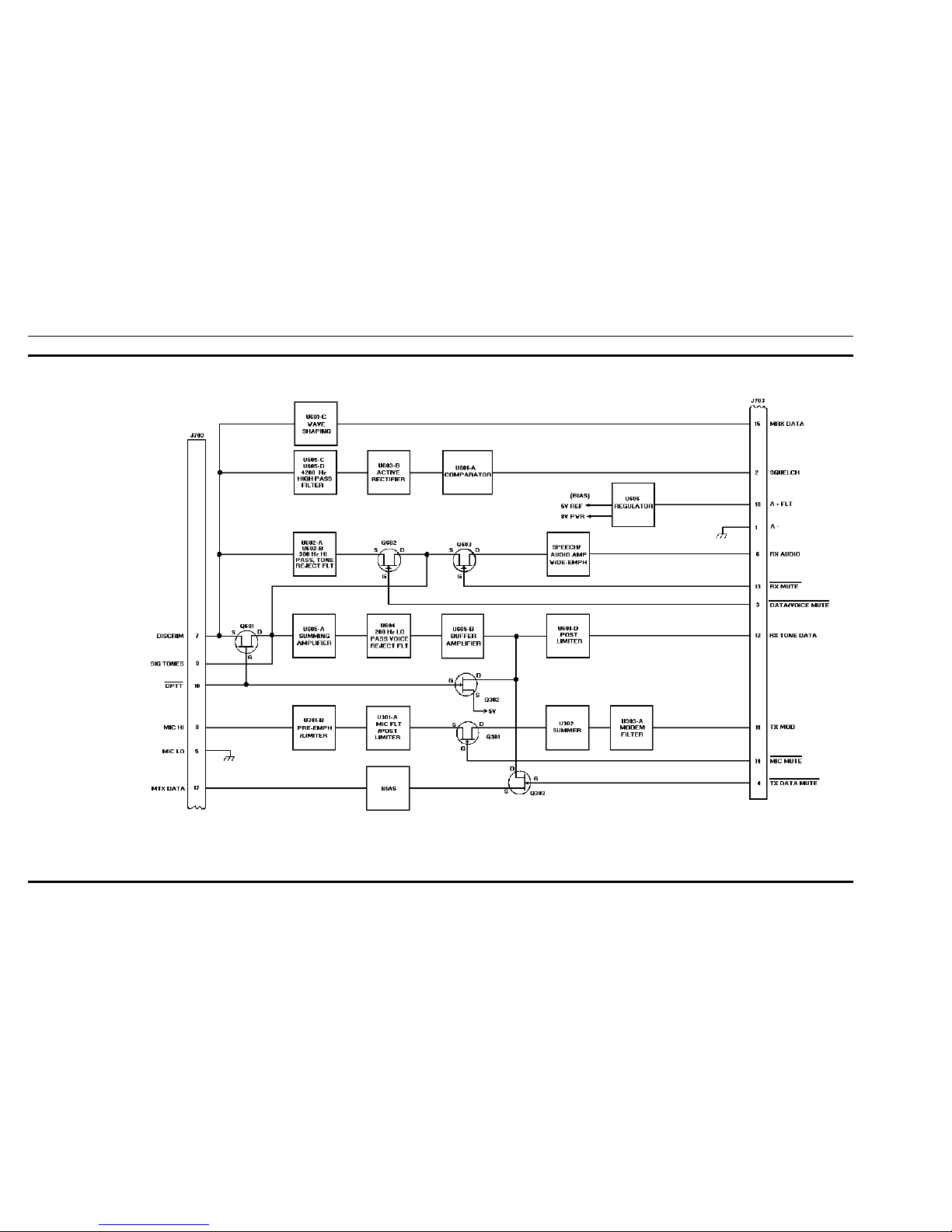
Figure 1 - Audio Board Blo ck Diagram
LBI-38546
2
Page 4

Figure 2 - Transmit Audio Circuits
LBI-38546
3
Page 5

Figure 3 - Receive Audio Circuits
LBI-38546
4
Page 6

PARTS LIST LBI-38546
5
Page 7

LBI-38546 OUTLINE DIAGRAM
(19D902304, Sh. 1, Rev. 3)
(19D902305, Component Side, Rev. 3)
COMPONENT SIDE
(19D902304, Sh. 1, Rev. 3)
(19D902305, Solder Side, Rev. 3)
SOLDER SIDE
6
Page 8

INTEGRATED CIRCUITS LBI-38546
OPERATIONAL AMPLIFIER
U301-U303, U602 & U603
19A700086P4
OPERATIONAL AMPLIFIER
U601
19A134764P1
OPERATIONAL AMPLIFIER
U604, U605
19A701789P1
VOLTAGE REGULATOR
U606
19A704073P2
7
Page 9

SCHEMATIC DIAGRAM LBI-38546
AUDIO BOARD
19D902304G2
(19D902306, Sh. 1, Rev. 10)
8
Page 10

SCHEMATIC DIAGRAM LBI-38546
AUDIO BOARD
19D902304G2
(19D902306, Sh. 2, Rev. 7)
9
 Loading...