

Ericsson 19D901841G3 Maintenance Manual
Printed in U.S.A.
MAINTENANCE MANUAL
851-870 MHz, 100 WATT POWER AMPLIFIER
19D901841G3
TABLE OF CONTENTS
Page
SPECIFICATIONS . . . . . . . . . . . . . . . . . . . . . . . . . . . . . . . . . . . . . . . . . . . . . . . Front Cover
DESCRIPTION . . . . . . . . . . . . . . . . . . . . . . . . . . . . . . . . . . . . . . . . . . . . . . . . . 1
CIRCUIT ANALYSIS . . . . . . . . . . . . . . . . . . . . . . . . . . . . . . . . . . . . . . . . . . . . . 1
Power Amplifier . . . . . . . . . . . . . . . . . . . . . . . . . . . . . . . . . . . . . . . . . . . . . 1
Power Control . . . . . . . . . . . . . . . . . . . . . . . . . . . . . . . . . . . . . . . . . . . . . . . 1
INTERCONNECTION DIAGRAM . . . . . . . . . . . . . . . . . . . . . . . . . . . . . . . . . . . . . . 2
OUTLINE DIAGRAMS
Power Amplifier . . . . . . . . . . . . . . . . . . . . . . . . . . . . . . . . . . . . . . . . . . . . . 4
Power Control Board . . . . . . . . . . . . . . . . . . . . . . . . . . . . . . . . . . . . . . . . . . . 6
Buffer Amplifier Assembly . . . . . . . . . . . . . . . . . . . . . . . . . . . . . . . . . . . . . . . . 10
SCHEMATIC DIAGRAMS
PowerAmplifier . . . . . . . . . . . . . . . . . . . . . . . . . . . . . . . . . . . . . . . . . . . . . . 5
Power Control Board . . . . . . . . . . . . . . . . . . . . . . . . . . . . . . . . . . . . . . . . . . . 7
Power Amplifier . . . . . . . . . . . . . . . . . . . . . . . . . . . . . . . . . . . . . . . . . . . . . 10
Power Amplifier Fan Assembly . . . . . . . . . . . . . . . . . . . . . . . . . . . . . . . . . . . . . 11
PARTS LIST . . . . . . . . . . . . . . . . . . . . . . . . . . . . . . . . . . . . . . . . . . . . . . . . . . 8
SPECIFICATIONS*
POWER OUTPUT 100 Watts (adjustable from 50 watts to rated power output).
FCC FILING AXATR-329
SPURIOUS AND HARMONIC EMISSION
(per EIA RS-152-B Par . 4)
-13dBm output (conducted)
-13dBm (Radiated)
DUTY CYCLE Continuous
RF OUTPUT IMPEDANCE 50 ohms
*These specifications are intended primarily for the use of the serviceman. Refer to the appropriate Specification Sheet for
the complete specifications.
Although the highest DC voltage supplied to the transmitter is + 24VDC, high currents may be drawn un de r short ci rc uit
conditions. These currents can heat metal objects such as tools, rings, watchbands, etc., enough to cause burns. Be careful
when working near energized 24 Volt circuits!
High level RF energy in the transmitter Power Amplifier assembly can cause RF burns upon contact. KEEP AWAY FROM
THESE CIRCUITS WHEN THE TRANSMITTER IS ENERGIZED!
WARNING
LBI-39030A

DESCRIPTION
The 19D901841G3 800 MHz power amplifier assembly
used in MASTR III station applications uses seven RF power
devices to provide a maximum of 100 watts output power. R11
on the Power Control Board (19D901803G3) provides adjustment of the output power over a 3 dB range (50W to 100W).
The power amplifier assembly consists of an RF board with
all the amplifier stages and an output detector, a power control
board, and an isolator. A driver amp board is also located on
the P.A. cover.
Supply voltage from the system board is connected to TB1
and decoupled by C6.
CIRCUIT ANALYSIS
DRIVER AMP
The driver amplifer board is located in a shielded enclosures mounted to the fan cover of the power amplifier assembly. This driver amp amplifie s the + 10dB (10mW) signal from
the Tx synthesizer to +20 dB (100mW).
The function of the 800 MHz Buffer Amplifier is to increase the power level from the MASTR III Exciter module to
a level sufficient to drive the 100 Watt MASTR II Power
Amplifier.
The circuit is powered from the T/R shelf’s +13 V supply.
This is connected to the board at J3.6, and powers the 8V
regulator, U1. The output of U1 is switched to the amplifier
circuit via Q2, which is turned on by a + 5V signal applied to
J3.2.
A +10 dBm RF signal is supplied at J2, and this drives the
MMIC, U2, via the attenuator network R9-R11. The output of
U2 drives the GaAs FET transistor , Q3. The nominal +20 dBm
output of U3 appears at J1.
POWER AMPLIFIER
The driver amp output (100mW) is coupled to the amplifier
input connector J1 by a 50 ohm coaxial cable. L1, C1, C2, and
the base microstrip form the input matching circuit for Q1.
Control voltage is applied to Q1 through a collector feed
network consisting of C3, C4, and L3.
Interstage matching between Q1 and Q2 is provided by L4,
L5, C6, C8, C9, and C10. Control voltage is applied to Q2
through a collector feed network consisting of Z1, C11-C13,
and L7. The output of Q2 is matched to the input of Q3 by L8,
L9, C30, C15, and the base microstrip.
Supply voltage for Q3 is applied through collector feed
network Z2, C16-C18, and L11. The output of Q3 is matched
to 50 ohms by microstrip W2. This output is applied to a
Wilkinson divider consisting of microstrips W4 and W5. R1
provides isolation between the signal paths.
Input matching for Q4 and Q5 is provided by microstrips
W8 and W9. Supply voltage is applied to Q4 and Q5 by
collector feed networks Z3, Z4, C20-C25, L12, and L13. Microstrips W12 and W13 provide output matching.
The outputs of Q4 and Q5 are summed by a Wilkinson
combiner consisting of W16, W17, and R3. The output of the
combiner is connected to pin 1 of circulator U1.
A directional coupler, W19, and detector CR1 provide a
voltage, proportional to the power out, to the power control.
POWER CONTROL
On the Power Control Board, the voltage from the detector
is compared to a stable DC reference voltage in a high gain
comparator, U2A. The comparator drives a DC amplifier, Q4
and pass transistor Q6 that supplies control voltage to the RF
board.
Thermistor RT1 is connected to the PA heatsink and, by
controlling the operation of Q2 and Q3, provides a power
cut-back for ambient temperatures that exceed 70 degrees
centigrade. Conduction of Q3 gradually decreases the power
set voltage applied to Q4. The DC reference voltage is provided
by Q1, U3, R17-19, and C5.
In other special applications of this power control board,
U2-B, CR1, and Q5 provide a low power alarm. U1 is used
to select one of four individually adjustable power levels.
In a MASTR III station application, the binary input
select lines of U1 are hardwired to select power level 0
(PLO), which is adjusted by R11. R2, R5, and R8 will have
no affect on the PA output power and should be set fully
CCW.
R1, R4, R7, and R10 are factory adjusted values.
Copyright© December 1993 Ericsson GE Mobile Communications Inc.
This amplifier is not field repairable. Should service
become necessary, the complete power amplifier
assembly must be returned to the factory for
servicing.
NOTE
The RF Power Transistors used in the transmitter
contain Beryllium Oxide, a TOXIC substance. If the
ceramic, or other encapsulation is opened, crushed,
broken, or abraded, the dust may be hazardous if
inhaled. Use care in replacing transistors of this type.
WARNING
LBI-39030 LBI-39030
1
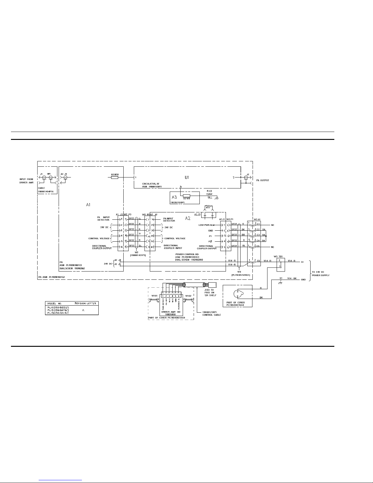
INTERCONNECTION DIAGRAN
POWER AMPLIFIER
19D901841G3
(19D902064, Sh. 1, Rev. 1)
LBI-39030 LBI-39030
2

INTERCONNECTION DIAGRAM
POWER AMPLIFIER
19D901841G3
(19D901841, Sh. 2, Rev._)
LBI-39030 LBI-39030
3
 Loading...