

Page 1
Printed in U.S.A.
MAINTENANCE MANUAL
851-870 MHz, 100 WATT POWER AMPLIFIER
19D901841G2
TABLE OF CONTENTS
Page
DESCRIPTION . . . . . . . . . . . . . . . . . . . . . . . . . . . . . . . . . . . . . . . . . . . . . . . . Front Cover
CIRCUIT ANALYSIS . . . . . . . . . . . . . . . . . . . . . . . . . . . . . . . . . . . . . . . . . . . . . Front Cover
Power Amplifier . . . . . . . . . . . . . . . . . . . . . . . . . . . . . . . . . . . . . . . . . . . . . Front Cover
Power Control . . . . . . . . . . . . . . . . . . . . . . . . . . . . . . . . . . . . . . . . . . . . . . 1
PARTS LIST . . . . . . . . . . . . . . . . . . . . . . . . . . . . . . . . . . . . . . . . . . . . . . . . . . 2
INTERCONNECTION DIAGRAM . . . . . . . . . . . . . . . . . . . . . . . . . . . . . . . . . . . . . . 4
OUTLINE DIAGRAMS
Power Amplifier . . . . . . . . . . . . . . . . . . . . . . . . . . . . . . . . . . . . . . . . . . . . . 5
Power Control Board . . . . . . . . . . . . . . . . . . . . . . . . . . . . . . . . . . . . . . . . . . . 7
SCHEMATIC DIAGRAMS
PowerAmplifier . . . . . . . . . . . . . . . . . . . . . . . . . . . . . . . . . . . . . . . . . . . . . . 6
Power Control Board . . . . . . . . . . . . . . . . . . . . . . . . . . . . . . . . . . . . . . . . . . . 8
DESCRIPTION
The 800 MHz po we r a mpli fie r a sse mbly u sed i n st ati on
applications u ses five RF power tra nsistors to provide a
maximum of 10 0 watts output power. R11 on th e Power
Control Boar d (19D 90180 3G3) p rovide s adjus tment o f the
output power ov er a 10 dB range (10W to 100 W) .
The power ampli fier asse mbly co nsists of an RF b oard
with all the amplifier stages and an output detector, a power
control board, a nd a n is o la to r.
Supply voltage from the system board is connected to
TB1 and decoupled by C6.
CIRCUIT ANALYSIS
POWER AMPLIFIER
The exciter output (65-130 mW) is coupled to the amplifier input conn ector J1 by a 50 o hm coaxial c able. L 1, C1,
C2, and the ba se m ic r os tr ip form the inpu t m a tc h in g c ir cuit
for Q1. Control voltage is applied to Q1 through a co ll e c to r
feed network consisti n g o f C3 , C4 , an d L3 .
Interstage matching between Q1 and Q2 is provided by
L4, L5, C6, C8, C9 , and C 10. C ont rol vo ltag e is app lied to
Q2 through a co lle c to r f e ed n etw o rk consisting of Z 1 , C11C13, and L7. The output of Q2 is matched to the input of Q3
by L8, L9, C30, C15, and the base microstri p .
Supply voltage for Q3 is applied through collector feed
network Z2, C16-C18, and L11. The output of Q3 is matched
to 50 ohms by microstrip W2. This output is applied to a
Wilkinson divider consisting of microstrips W4 and W5. R1
provides isola ti on between the sig na l p at h s.
Input matching for Q4 and Q5 is provided by microstrips
W8 and W9. Supply vo ltage is applied to Q4 and Q 5 by
collector feed n etworks Z3, Z4 , C20-C25, L12, a nd L13.
Microstrips W1 2 and W13 provide ou tp u t ma tc hing.
The outputs o f Q4 and Q 5 are su mmed by a Wilki nson
combiner consisting of W16, W17, and R3. The output of the
combiner is conne ct e d to pi n 1 o f ci r cu la tor U1.
LBI-38134C
Page 2
A directional coupler, W19, and detector CR1 provide a
voltage, propo rti o na l t o th e power out, to the powe r c on tro l.
POWER CONTROL
On the Power Control Board, the voltage from the detector
is compared to a stable D C reference v oltage in a h igh gain
comparator, U2A. The c om parato r d riv es a DC amp lif ier, Q4
and pass transis tor Q6 t hat s upp lies contr ol vo lta ge to the RF
board.
Thermistor RT1 is conne cted to the PA heatsink and, by
controlling the operation of Q2 and Q3, provides a power
cut-back for a mbient temperatures that e xceed 70 degrees
centigrade. C onductio n of Q3 gradua lly dec reases the p ower
set voltage applied to Q4. The DC reference voltage is provided
by Q1, U3, R17-19, a nd C5 .
In other special a pplicatio ns of this p ower contr ol board,
U2-B, CR1, and Q5 pr ov id e a lo w po wer ala rm . U1 is used to
select one of fou r in d iv i dually adjustabl e power levels.
R1, R4, R7, and R1 0 ar e fa ct o ry adjusted values.
Copyright© August 1987, General Electric Company
This amplifier is not field repairable. Should service
become necessary, the complete power amplifier
assembly must be returned to the factory for servicing.
NOTE
The RF Power Transistors used in the transmitter contain
Beryllium Oxide, a TOXIC substance. If the ceramic, or
other encapsulation is opened, crushed, broken, or
abraded, the dust may be hazardous if inhaled. Use care
in replacing transistors of this type.
WARNING
LBI-38134 LBI-38134
1
Page 3
851-870 MHZ 100 WATT POWER AMPLIFIER
19D901841G2
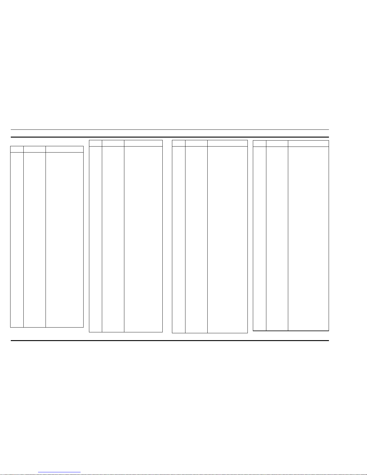
PARTS LIST
SYMBOL PARTS LIST DESCRIPTION
A1 POWER AMPLIFIER BOARD
19D901807G3
— — — CAPACITORS — — —
C1 19A702232P12
Ceramic: 9.1 pF ±5%, 50 VDCW.
C2 19A705108P13
Mica Chip: 10 pF ±5%, 500 VDCW,
temp coef 0 + 200 PPM/°C.
C3 19A702232P31
Ceramic: 56 pF ±5%, 50 VDCW.
C4 19A702250P113
Polyester: 0.1 µF ±10%, 50 VDCW.
C6 19A702232P3
Ceramic: 3.9 pF ±.25 pF, 50 VDCW.
C7 19A702232P31
Ceramic: 56 pF ±5%, 50 VDCW.
C8 19A705108P13
Mica Chip: 10 pF ±5%, 500 VDCW,
temp coef 0 + 200 PPM/°C.
C9
and
C10
19A705108P13
Mica Chip: 10 pF ±5%, 500 VDCW,
temp coef 0 + 200 PPM/°C.
C11 19A702232P31
Ceramic: 56 pF ±5%, 50 VDCW.
C12 19A702250P113
Polyester: 0.1 µF ±10%, 50 VDCW.
C13 19A701534P6
Tantalum: 4.7 µF ±20%, 35 VDCW.
C14 19A702232P31
Ceramic: 56 pF ±5%, 50 VDCW.
C15 19A705108P9
Mica: 6.8 pF ±.25 pF, 500 VDCW.
C16 19A705108P25
Mica Chip: 33 pF ±5%, 500 VDCW,
temp coef 0 + 50 PPM/°C.
C17 19A702250P113
Polyester: 0.1 µF ±10%, 50 VDCW.
C18 19A701534P6
Tantalum: 4.7 µF ±20%, 35 VDCW.
C19 19A702232P31
Ceramic: 56 pF ±5%, 50 VDCW.
C20
and
C21
19A705108P25
Mica Chip: 33 pF ±5%, 500 VDCW,
temp coef 0 + 50 PPM/C.
C22 19A701534P6
Tantalum: 4.7 µF ±20%, 35 VDCW.
C23
and
C24
19A702250P113
Polyester: 0.1 µF ±10%, 50 VDCW.
C25 19A701534P6
Tantalum: 4.7 µF ±20%, 35 VDCW.
C26
and
C27
19A702232P31
Ceramic: 56 pF ±5%, 50 VDCW.
C28 19A702232P21
Ceramic: 22 pF ±5%, 50 VDCW.
C29 19A702232P1
Ceramic: 3.3 pF ±.25 pF, 50 VDCW.
C30 19A705108P8
Mica: 6.2 pF ±.25 pF, 500 VDCW.
C31
thru
C35
19A705108P25
Mica Chip: 33 pF ±5%, 500 VDCW,
temp coef 0 + 50 PPM/°C.
— — — — DIODES — — — —
CR1
and
CR2
19A700047P3 Silicon: 100 mW; sim to 1N6263.
— — — — JACKS— — — — —
J1 19A700049P2 Connector, receptacle; 500 VDCW
maximum; sim to NTTF-1058.
J2 Part of Circulator U1.
J3 19A704852P32 Printed wire, two part: 6 contacts, sim
to Molex 22-29-2061.
J4
and
J5
19A134263P1 Contact, electrical: sim to Selectro
229-1082-00-0-590.
*
COMPONENTS ADDED, DELETED OR CHANGED BY PRODUCTION CHANGES
SYMBOL PARTS LIST DESCRIPTION
— — — INDUCTORS — — — —
L1 Part of printed wire board.
L2 19A701091G1 Coil.
L3 19A701091G1 Coil.
L4 19A701006P7 Strap.
L5 Part of printed wire board.
L6 19A701091G1 Coil.
L7 19A136533P2 Coil.
L8
and
L9
Part of printed wire board.
L10 19A701091G1 Coil.
L11
thru
L13
19A136533P2 Coil.
— — — TRANSISTORS— — — —
Q1 19A703479P1 N Channel, field effect. sim to RF
2060.
Q2 19A703480P4 Silicon, NPN: Sim to MRF-891.
Q3 19A705125P1 Silicon, NPN: Sim to MRF-895.
Q4
and
Q5
19A705125P2 Silicon, NPN: Sim to MRF-898.
— — — RESISTORS — — — —
R1 19A700111P39
Composition: 100 ohms ± 5%, 2 w.
R2 19A700106P32
Composition: 51 ohms ± 5%, 1/4 w.
R3 19A143832P1
Power: 100 ohms ±5%, 75 w.
R4 19A700113P55
Composition: 470 ohms ± 5%, 1/2
w.
R5 H212CRP247C
Deposited carbon: 4.7K ohms ±5%,
1/4 w.
R6 H212CRP310C
Deposited carbon: 10K ohms ±5%, 1/4
w.
R7 19A700106P55
Composition: 470 ohms ± 5%, 1/4 w.
R8 19B800607P101
Metal film: 100 ohms ±5%, 1/8 w.
— INTEGRATED CIRCUITS — —
U1 19B802097P2 Circulator: 120 watts.
— — — — CABLES — — — — —
W1
thru
W20
Part of printed wire board.
— — — — FILTER — — — — —
Z1
thru
Z4
19A701092G1 Filter.
19B801426P2 Support plate.
19B801426P1 Support plate.
A2 POWER CONTROL BOARD
19D901803G3
— — — CAPACITORS — — — —
C1
thru
C4
19A700233P9
Ceramic: 2200 pF ±20%, 50 VDCW.
SYMBOL PARTS LIST DESCRIPTION
C5 T644ACP310K
Polyester: .010 µF ±10%, 50 VDCW.
C6 19A701534P6
Tantalum: 4.7 µF ±20%, 35 VDCW.
C7 19A701624P12
Ceramic, disc: 15 pF ±5%, 500 VDCW,
temp coef 0 PPM ±30.
C8 19A702250P113
Polyester: 0.1 µF ±10%, 50 VDCW.
C9
thru
C12
19A701624P12
Ceramic, disc: 15 pF ±5%, 500 VDCW,
temp coef 0 PPM ±30.
C13 19A700233P6
Ceramic: 680 pF ±20%, 50 VDCW.
— — — — DIODES— — — — —
CR1 19A700028P1 Silicon: 75 mA, 75 PIV; sim to 1N4148.
— — — — — JACKS — — — — —
J1 19A704852P31 Connector: 5 contacts; sim to Molex 22-
29-2051.
J2 19A704852P32 Printed wire, two part: 6 contacts, sim to
Molex 22-29-2061.
J3 19A700072P1 Printed wire: 2 contacts rated @ 2.5
amps; sim to Molex 22-03-2021.
— — — TRANSISTORS — — —
Q1 19A700023P2 Silicon, NPN: sim to 2N3904.
Q2
and
Q3
19A700022P2 Silicon, PNP: sim to 2N3906.
Q4
and
Q5
19A700023P2 Silicon, NPN: sim to 2N3904.
Q6 19A700055P1 Silicon, PNP. (Included with Heat Sink
Assembly 19B801427G4).
Q7
and
Q8
19A700023P2 Silicon, NPN: sim to 2N3904.
— — — — RESISTORS — — — —
R1 19A134248P4 Variable, cermet, 4 turns: 25K ohms
±10%, 1/2 w; sim to Bourns 3339P-1-
253.
R2 19B800779P10
Variable: 10K ohms ±25%, 100 VDCW,
.3 watt.
R3 H212CRP210C
Deposited carbon: 1K ohms ±5%, 1/4 w.
R4 19A134248P4 Variable, cermet, 4 turns: 25K ohms
±10%,1/2 w; sim to Bourns 3339P-1-253.
R5 19B800779P10
Variable: 10K ohms ±25%, 100 VDCW,
.3 watt.
R6 H212CRP210C
Deposited carbon: 1K ohms ±5%, 1/4 w.
R7 19A134248P4 Variable, cermet, 4 turns: 25K ohms
±10%, 1/2 w; sim to Bourns 3339P-1-
253.
R8 19B800779P10
Variable: 10K ohms ±25%, 100 VDCW,
.3 watt.
R9 H212CRP210C
Deposited carbon: 1K ohms ±5%, 1/4 w.
R10 19A134248P4 Variable, cermet, 4 turns: 25K ohms
±10%, 1/2 w; sim to Bourns 3339P-1-
253.
R11 19B800779P10
Variable: 10K ohms ±25%, 100 VDCW,
.3 watt.
R12 H212CRP210C
Deposited carbon: 1K ohms ±5%, 1/4 w.
R13
and
R14
H212CRP310C
Deposited carbon: 10K ohms ±5%, 1/4
w.
R15 H212CRP415C
Deposited carbon: 0.15M ohms ±5%,
1/4 w.
R16 H212CRP368C
Deposited carbon: 68K ohms ±5%, 1/4
w.
R17 19A701250P239
Metal film: 2490 ohms ±1%, 250 VDCW,
1/4 watt.
SYMBOL PARTS LIST DESCRIPTION
R18 19A701250P295
Metal film: 9.53K ohms ±1%, 1/4 w.
R19 H212CRP168C
Deposited carbon: 680 ohms ±5%, 1/4 w.
R20
and
R21
H212CRP310C
Deposited carbon: 10K ohms ±5%, 1/4 w.
R22 H212CRP247C
Deposited carbon: 4.7K ohms ±5%, 1/4
w.
R23 H212CRP222C
Deposited carbon: 2.2K ohms ±5%, 1/4
w.
R24 H212CRP310C
Deposited carbon: 10K ohms ±5%, 1/4 w.
R25 H212CRP233C
Deposited carbon: 3.3K ohms ±5%, 1/4
w.
R26 H212CRP239C
Deposited carbon: 3.9K ohms ±5%, 1/4
w.
R27 H212CRP218C
Deposited carbon: 1.8K ohms ±5%, 1/4
w.
R28 H212CRP256C
Deposited carbon: 5.6K ohms ±5%, 1/4
w.
R29 H212CRP227C
Deposited carbon: 2.7K ohms ±5%, 1/4
w.
R30 H212CRP268C
Deposited carbon: 6.8K ohms ±5%, 1/4
w.
R31 H212CRP210C
Deposited carbon: 1K ohms ±5%, 1/4 w.
R32 H212CRP147C
Deposited carbon: 470 ohms ±5%, 1/4 w.
R33 19A143832P
Power: 50 ohms ±5%, 150 watts. (Used
with A3).
R34 H212CRP439C
Deposited carbon: 0.39M ±5%, 1/4 w.
R35 H212CRP347C
Deposited carbon: 47K ohms ±5%, 1/4 w.
— — — THERMISTOR — — — —
RT1 19A702176G2
Thermistor: 40K ohms ±20%.
— INTEGRATED CIRCUITS — —
U1 19A700029P36 Digital: Single 8-Channel Multiplexer; sim
to 4051B.
U2 19A701789P2 Linear: Dual Op Amp; sim to LM358.
U3 19A702939P2 Linear: Adjustable Shunt Regulator; sim
to TL431CLP.
— — MISCELLANEOUS — — —
19A702364P305 Machine screw: TORX DRIVE, M3-.5 x 5.
19B801427G4 Heat Sink Assembly. Includes Q6 and:
19A700115P3 Insulator, plate.
19A700068P1 Insularor, bushing.
19B801428G3 Heat Sink.
N404P11B6 Lockwasher; internal: No. 4.
N402P5B6 Washer: narrow, steel.
N80P9005B6 Machine screw: pan head, steel.
A3 PRINTED WIRE BOARD
— — — — CABLES — — — — —
W1 19A705075P1 Cable.
W2 19B801431P3 Cable.
W3 19C851528G1 Cable. (Includes Feed-thru Plate,
connector P1 and associated hardware).
— — MISCELLANEOUS — — —
19B801424G1 Frame.
19B801423G3 Plate.
19B226212G1 Heat Sink. (Mounts on Plate, Qty of 4).
LBI-38134 LBI-38134
2
Page 4

PARTS LIST
SYMBOL PARTS LIST DESCRIPTI ON
19B226212G5 Heat Sink. (Mounts on Plate, Qty of 1).
NP280071 Nameplate. (CAUTION).
19B209103P410 Tap screw, hex head: No. 8-32 x 5/8.
(Secures Heat Sink to plate).
19B201074P308 Tap screw, Phillips POZIDRIV: No. 6-32
x 1/2. (Used with A1, Q4, Q5 and
ground strap).
19B209103P306 Tap screw, hex head: No. 6-32 x 3/8.
(Secures frame to plate).
N403P13B6 Lockwasher: No. 6. (Used with ground
strap).
N81P9012 Machine screw, recessed pan: No. 4-40
x 3/4.
N414P11 Lockwasher, internal tooth: No. 4.
(Used with Circulator).
N44P9006B6 Machine screw, fillister head. (Secures
Q2-Q5).
N405P5B6 Lockwasher. (Used with Q2-Q5, R3 and
R33).
5492178P2 Washer, spring tension: sim to Wallace
Barnes 375-20. (Used with Q1).
19A148323P1 Heat Sink. (Used with Q1).
N210P15B6 Nut, hex: No. 8-32. (Used with Q1).
N402P8B6 Flatwasher, steel: No. 8. (Used with Q1).
19C851552P1 Guide. (Used around potentiometers on
A2).
19B201074P320 Tap screw, Phillips POZIDRIV: No. 6-32
x 1-1/4. (Secures A2 Q6 Heat Sink).
19A705329P1 Temperature indicator: sim to Tempil
Division of Big Three Industries Cat. No.
BU-175/79. (Attached to A1 Q4).
19A116552P3 Cable clip: sim to Richco KKC-4.
(Supports W3).
19A705097G1 Support. (Used with input connector J1).
N80P13004B6 Screw, machine: Pan head; No. 6-32 x
1/4". (Secures support).
19D438235G7 Fan Assembly, 24 Vdc.
19A701863P13 Cable clip. (Secures fan assembly
wiring).
7141225P2 Nut, Hex: 4-40. (Secures cable clip).
N80P13006B6 Machine screw: Pan head, Phillips; No.
8-32 x 3/8"
N404P13B6 Lockwasher, internal tooth: No. 6.
N402P7B6 Flatwasher, narrow: No. 6.
7141225P3 Hex Nut: No. 6-32.
N80P9005B6 Machine screw, pan head, steel, No. 4-
40UNC x 5/16".
N402P5B6 Washer: narrow, steel.
N404P11B6 Loackwasher, internal tooth, No. 4.
PRODUCTION CHANGES
Changes in the equipment t o improve performance or to simplify
circuits are identified by a "Revision Letter" which is stamped after
the model number of the unit. The revision stamped on the unit
includes all previous revision s. Re fer to the Pa r ts L ist for th e d esc ri ptions of parts affected by these revisions.
REV. A -
POWER AMPLIFIER 19D901807G3
To allow maximum power transfer from the exciter, changed C2 and L4,
deleted R6 and added R7.
C2 was 19A705108P15 Mica: 12pF ±5%, 500 VDCW.
L4 was 19A701006P6 Strap.
R6 was H212CRP310C Deposited carbon: 10K ±5%, 1/4 w.
REV. B -
POWER AMPLIFIER 19D901807G3
To improve power cutoff when no RF is present at the input. Changed R5
and added R6.
R5 was H212CRP318C Deposited carbon: 18K ±5%, 1/4 w.
REV. C -
POWER AMPLIFIER 19D901807G3
To improve stability, added R8.
REV. A -
POWER CONTROL BOARD 19D901803G3
To allow alarming of a low or missing drive level to the Power Amplifier,
changed R15, R16, R35 and Q8. Changed R34 and relocated as shown
below. Also changed R1, R4, R7 and R10 from a 1 turn potentiometer to
a 4 turn potentiometer.
R1 is 19A134248P4 - Variable, cermet, 4 turns: 25K o h ms ±10%, 1/2 w;
sim to Bourns 3339P-1-253.
R4 is 19A134248P4 - Variable, cermet, 4 turns: 25K ohms ±10%, 1/2 w;
sim to Bourns 3339-1-253.
R7 is 19A134248P4 - Variable, cermet, 4 turns: 25K ohms ±10%, 1/2 w;
sim to Bourns 3339P-253.
R10 is 19A134248P4 - Variable, cermet, 4 tu rns: 25K oh ms ±10%, 1/2
w; sim to Bourns 3339P-1-253.
R15 is H212CRP415C - Deposited carbon: .15M ohms ±5%, 1/4 w.
R16 is H212CRP368C - Deposited carbon: 68K ohms ±5%, 1/4 w.
R34 is H212CRP439C - Deposited carbon: .39M ohms ±5%, 1/4 w.
R35 is H212CRP347C - Deposited carbon: 47K ohms ±5%, 1/4 w.
Q8 is 19A700023P2 - Silicon, NPN: sim to 2N3904.
LBI-38134 LBI-38134
3
Page 5

INTERCONNECTION DIAGRAM
POWER AMPLIFIER
19D901841G2
(19D902064, Sh. 1, Rev. 1)
LBI-38134 LBI-38134
4
Page 6

POWER AMPLIFIER
19D901807G3
(19D901807, Sh. 2, Rev. 6)
(19D705468, Sh. 1, Rev. 3)
(19A705468, Sh. 2, Rev. 1)
OUTLINE DIAGRAM
COMPONENT SIDE
LBI-38134 LBI-38134
5
Page 7

SCHEMATIC DIAGRAM
POWER AMPLIFIER
19D901807G3
(19D902062, Rev. 4)
LBI-38134 LBI-38134
6
Page 8

OUTLINE DIAGRAM
COMPONENT SIDE
SOLDER SIDE
POWER CONTROL BOARD
19D901803G3
(19D901803, Sh. 1, Rev. 1)
(19D902059, Component Side, Rev. 1)
(19D902059, Solder Side, Rev. 1)
LBI-38134 LBI-38134
7
Page 9

SCHEMATIC DIAGRAM
POWER CONTROL BOARD
19D901803G3
(19D902060, Sh. 1, Rev. 11)
LBI-38134 LBI-38134
8
Page 10

This page intentionally left blank
LBI-38134 LBI-38134
9
 Loading...