

Page 1
Mobile Communications
VEHICULAR CHARGER/
REPEATER UNIT
19B801507P2
Printed in U.S.A.
Maintenance Manual
LBI-31869A
Page 2
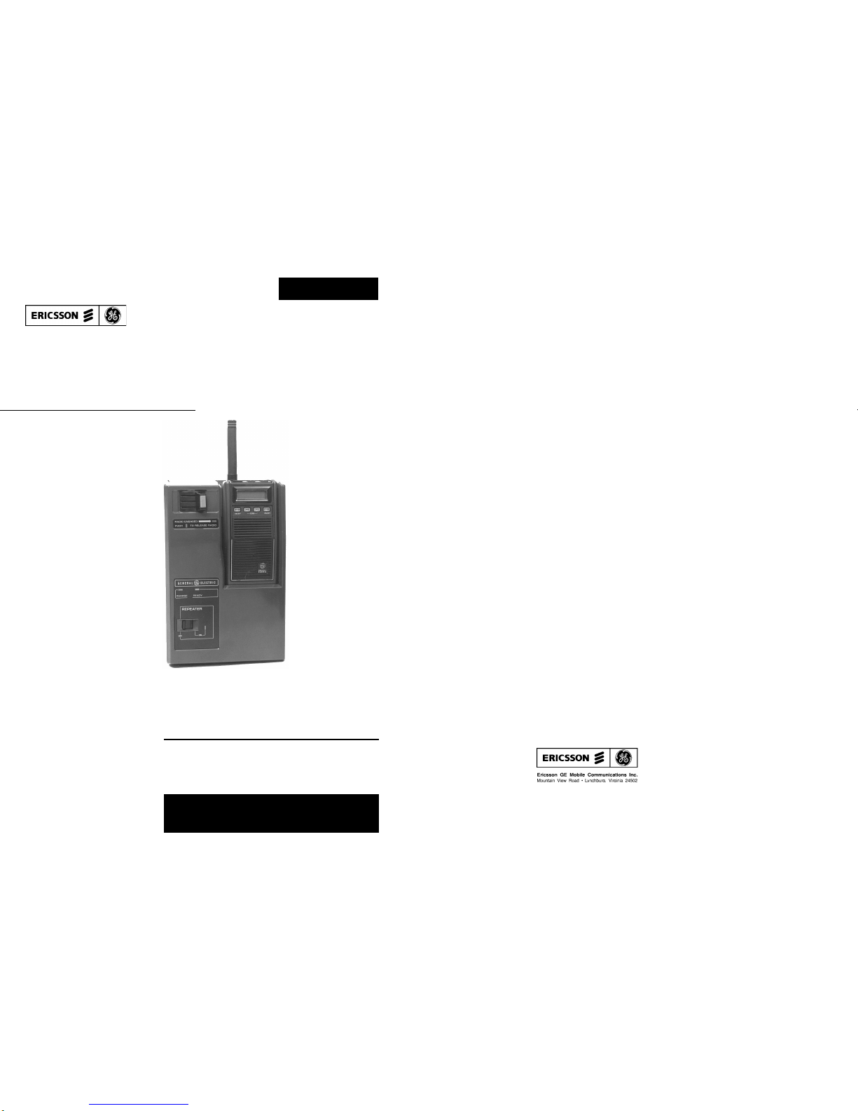
DESCRIPTION
General Electric Vehicular Charger/Repeater units provide the charging facility for the portable radio unit and the
Vehicular Repeater System enable/disable function. The
portable radio unit battery pack will be charged as long as
the radio is inserted i nto the charging compartment. The
Vehicular Repeater System is automatically disabled whenever the portable radio unit is inserted into the charging
compartment. It will recharge either the standard high, or
extra high capacity nickel-cadmium batteries.
The charging contacts are automatically connected
when the radio is inserted into the charger. Radio detect
switch S1, located in the battery compartment, applies power
to the charging circuit when the radio is inserted. A second
switch senses the size of the battery pack and adjusts the
charging rate accordingly.
Heat sensors constantly monitor the temperature of both
the battery pack and the charging insert. When a cold battery
pack is inserted into the charging insert, the charger will wait
until the battery pack has warmed up to within about 10°C
of ambient. The charger will then, automatically, ap pl y t he
high charge rate. When the battery pack overcharges enough
to heat the cells 10°C above ambient, the charger will switch
from fast charge to trickle charge.
The charger also has a memory that is set when the
charger switches from the high charging rate to the trickle
charge rate and is reset when the battery pack is removed
from the charging insert. If a hot battery is in the charging
insert and the memory has not been reset, the charger will
remain at the trickle charge rate. If the memory has been reset
the charger will wait until the battery pack has cooled before
automatically switching to fast charge. If a fully charged
battery pack is removed from the charging insert and then
reinserted, it will charge for about 1/2 hour until the battery
pack reheats.
A voltage cut-off circuit has also been incorporated to
prevent overcharging and "gassing" of the battery pack.
Battery voltage is constantly monitored and, if the battery
pack charge terminal voltage exceeds 9.5 volts, high rate
charge is terminated and the LED READY light is turned on.
If the radio is on when it is in the charger, it is powered
from the radio battery while it is being charged. If the radio
is OFF while it is in the charger, it is inoperative; the battery
is charged if either condition exists.
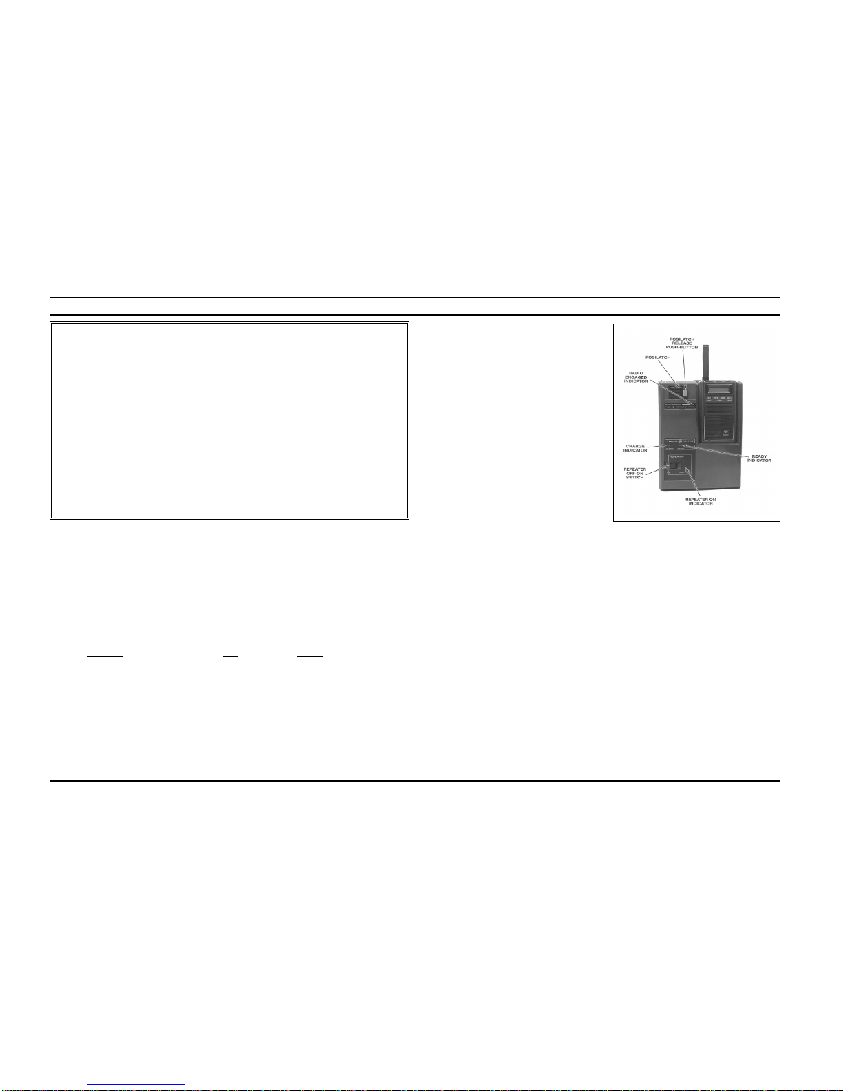
CONTROLS AND INDICATORS
Four switches and four indicators provide control and
status information for the Vehicular Cha rger. Refer to Figure
1 for location of controls and indicators.
RADIO ENGAGED (RED) Lights when the radio is
inserted properly into the
charger and the radio i s
latched.
CHARGE (red) Indicates the battery is
being charged.
READY (GREEN) Indicates the battery is
fully charged. The
charger will automatically switch from a rapid
charge rate to a trickle
charge rate.
REPEATER ON-OFF (yellow) Indicates the repeater is
on.
S1 Radio Detect Closes when the radio is
inserted into the charger.
Applies battery voltage
to Charger Control circuit and Repeater Display board.
S2 Battery Set Resets the power off and
memory circuit.
Copyright © September 1987, General Electric Company
TABLE OF CONTENTS
SPECIFICATIONS . . . . . . . . . . . . . . . . . . . . . . . . . . . . . . . . . . . . . . . . . . . . . . . . . . 1
DESCRIPTION . . . . . . . . . . . . . . . . . . . . . . . . . . . . . . . . . . . . . . . . . . . . . . . . . . . 1
OPERATION . . . . . . . . . . . . . . . . . . . . . . . . . . . . . . . . . . . . . . . . . . . . . . . . . . . . . 2
CIRCUIT ANALYSIS . . . . . . . . . . . . . . . . . . . . . . . . . . . . . . . . . . . . . . . . . . . . . . . . 2
CHARGER BOARD . . . . . . . . . . . . . . . . . . . . . . . . . . . . . . . . . . . . . . . . . . . . . . 2
DISPLAY REP . . . . . . . . . . . . . . . . . . . . . . . . . . . . . . . . . . . . . . . . . . . . . . . . . 3
INSTALLATION . . . . . . . . . . . . . . . . . . . . . . . . . . . . . . . . . . . . . . . . . . . . . . . . . . . 3
MAINTENANCE . . . . . . . . . . . . . . . . . . . . . . . . . . . . . . . . . . . . . . . . . . . . . . . . . . 3
DISASSEMBLY PROCEDURES . . . . . . . . . . . . . . . . . . . . . . . . . . . . . . . . . . . . . . . 3
ADJUSTMENT PROCEDURES . . . . . . . . . . . . . . . . . . . . . . . . . . . . . . . . . . . . . . . . 4
TROUBLESHOOTING PROCEDURES . . . . . . . . . . . . . . . . . . . . . . . . . . . . . . . . . . . 4
TEST ADAPTOR . . . . . . . . . . . . . . . . . . . . . . . . . . . . . . . . . . . . . . . . . . . . . . . . . . 5
LIST OF TABLES
TABLE 1 - QUICK CHECKS . . . . . . . . . . . . . . . . . . . . . . . . . . . . . . . . . . . . . . . . . . . . 4
TABLE 2 - EQUIPMENT STATUS . . . . . . . . . . . . . . . . . . . . . . . . . . . . . . . . . . . . . . . . . 4
TABLE 3 - VOLTAGE READINGS . . . . . . . . . . . . . . . . . . . . . . . . . . . . . . . . . . . . . . . . 4
SPECIFICATIONS*
INPUT POWER 11.1 TO 16.5 Volts
DC, negative ground
CURRENT DRAIN 1.7 A maximum
INPUT CURRENTS
Standby 1 mA maximum
Radio Squelched, Trickle Charge 100 mA maximum
Radio Squelched, Rapid Charge 1700 mA maximum
CHARGE TIME
Standard High Capacity 3 Hours
Extra High Capacity 4 Hours
CHARGE CAPACITY AND TIME VS TEMPERATURE (Standard High Capacity)
Temperature Time Capacity
+5°C (+41°F) 3.3 Hours 100%
+25°C (+77°F) 3.0 Hours 100%
+45°C (+113°F) 2.7 Hours 70%
INDICATORS
Radio Engaged Red
Charge Red
Repeater ON Yellow
DIMENSIONS.(H x W x D) 22.6 x 15 x 7 cm
(8.9 x 5.9 x 2.7 ins.)
WEIGHT 1.4 kG (3.1 lb)
* These specifications are intended primarily for the use of the service technician.
Figure 1 - Veh icular Charge r
LBI-31869 LBI-31869
1
Page 3

S3 Radio Engaged C loses when r adio i s
properly inserted into
charging insert and applies power to DS1, RADIO ENGAGED
indicator.
S1 Repeater OFF-ON ON: Enables Vehicular
Repeater function if radio is not inserted into
charging compartment.
OFF: Vehicular Repeater
System is disabled.
OPERATION
Temperature characteristics of nickel-cadmium batteries, prevent a full charge at temperature extremes. For maximum charge, recharge the battery pack at ambient room
temperature or between 65° and 85°F.
CHARGER/REPEATER OPERATION
The following procedures describe the recharging of the
portable radio battery pack and the operation of the Vehicular
Repeater System.
1. The power switch on the radio battery pack may be
in the ON or OFF position.
2. Insert radio unit into charging compartment with its
speaker facing forward (see Figure 2.).
3. Slide the PO SILATCH
TM
toward the portable radio
unit until you feel it engage and the red RADIO
ENGAGED indicator lights.
4. Place the REPEATER ON OFF switch to the ON
position. The red repeater ON indicator will not light
until the portable radio is removed from the charging
compartment.
5. The red CHARGE indicator will light and remain lit
until the portable radio unit is removed or until the
vehicular repeater/charger unit circuits sense that the
battery pack has reached total charge capacity. At this
time the green READY indicator will also light,
indicating that the charger has switched to th e trickle
charge rate.
6. To remove the portable radio from the charging
compartment, depress the blue push-button release
on the POSILATCH and sli de the latch completely
away from the portable radio unit. The red RADIO
ENGAGED indicator will turn off and the portable
radio unit can be removed from the charging compartment (see Figure 2).
7. Removing the portable radio unit will automat i ca lly
enable the Vehicular Repeater System and the red
REPEATER ON indicator will light.
CIRCUIT ANALYSIS
The Vehicular Charger is comprised of a Charger board,
LED board, Display Repeater board, and a UDC board.
CHARGER BOARD
The Charger board contains the charging circuit, with
voltage and temperature cut-off circuits.
CHARGING CIRCUIT
When power is first applied to the charger, the voltage at
pin 5 of Comparator A7 is higher than at pin 6 of A7 due to the
charging time of C18. The higher voltage causes the output at
pin 7 of A7 to go high, keeping A13 turned off. This allows the
battery to start charging. A block diagram of the Vehicular
Charger is shown in Figure 3.
Charging current flows through series connected resistors
R21 and R22 to regulator transistor Q3. The output of Q3 i s
connected to the positive charging contact of the battery. Test
Point TP2 provides a convenient
place to monitor the positive battery contact. A portion of the
charging current is routed through resistor R24 and transistor
Q2 to turn on CHARGE LED DS3 on the LED board and to
provide a trickle charge when Q2 turns off. The series connected charge circuit determines the high charge rate and is
controlled by the temperature controlled cut-off circuit.
CHARGER CONTROL CIRCUIT
The Charger Control circuit consists of a temperature
controlled cut-off circuit and battery charged memory circuit.
The temperature controlled cut-off circuit consists of integrated circuit A13, a bridge circuit comprised of R29, R30,
R33, thermistors RT1 and RT (B ATT), and associated circuitry.
Temperature cut-off IC A13 monitors the temperature of the
charging insert through thermistor RT1 and the temperature of
the battery pack through internal thermistor RT (B AT T). It also
controls transistors Q3 and Q4, turns the "READY" indicator
on when the battery pack is fully charged, and provides memory to prevent the same battery pack from being recharged a t
the high rate.
Thermistors RT1 and R T (BATT) are connected with R29,
R30, and R33 to form a bridge circuit (see Figure 4). The output
of the bridge circuit is connected to terminals 13 and 14 of A13.
The General Electric Vehicular Charger is designed
to recharge the GE standard high capacity battery
pack and the extra high capacity battery pack. Attempting to recharge any other battery pack or batteries may result in damage to equipment, leakage,
or explosion.
WARNING
NOTE
The REPEATER OFF-ON switch must be in the
ON position for the Vehicular Repeater System to
function.
NOTE
When the portable radio unit is placed in the charging insert, set the REPEATER OFF-ON switch to
ON so the Vehicular Repeater System will be enabled automatically when the portable radio is removed from the charger.
DO NOT use the antenna to remove the portable
radio from the charging compartment.
CAUTION
NOTE
The Vehicular Repeater System will be disabled as
long as the portable radio unit is in the charging
compartment or the REPEATER OFF-ON switch is
in the OFF position.
Figure 2 - Inserting and Removing Portable Radio Unit
LBI-31869 LBI-31869
2
Page 4

When the battery pack temperature is more than 10°C
(18°F.) below ambient, thermistor RT (BATT) exhibits a high
resistance, causing the voltage on A13-13 to be larger than the
voltage on A13-14. (The same thing would occur if there were
no battery pack present). There is no output from A13-6 or
A13-10. Transistor Q3 and LED READY indicator DS2 remain
off. The battery pack charges at the trickle charge rate, determined by series resistance R24, until the temperature is less
than 10°C below ambient. At less than 10°C below ambient,
the voltage at A13-13 is still larger than the voltage on A13-14,
the output at A13-6 goes high causing transistor Q4 to conduct,
turning Q3 on and beginning the high-rate charge.
As the battery pack temperature increases to 10°C above
ambient at end of charge, the voltages at A13-13 and A13-14
become equal, indicating the bridge circuit is balanced and the
battery pack is fully charged. A14-6 goes low, causing Q4 to
stop conducting. Q3 cuts off and the charge rate switches from
the high charge rate to the trickle charge rate . The equal
voltages on A13-13 and A13-14 cause the output at A13-10 to
go high, turning READY indicator DS2 on.
A memory circuit internal to A13 is set so that the same
battery can not be recharged at the high rate unless it first has
been discharged or removed from the charger. When the battery
pack is removed from the charging insert, RT (BATT) is removed from the bridge circuit causing the bridge to again be
unbalanced. A13 senses the bridge in an unbalanced state, the
voltage A13-13 being larger than the voltage on A13-14, and
resets the charger memory. Microswitch S1 (RADIO DETECT) will also remove power from the charger circuits,
causing the memory to reset.
VOLTAGE CONTROLLED CUT-OFF
The voltage controlled cut-off circuit monitors the battery
voltage and cuts off regulator Q3 when the battery charging
terminal voltage exceeds 9.5 Vdc. It is comprised of Comparator A7, Charge Control IC A13, and associated circuitry.
A reference voltage derived from voltage divider R37,
R38, R41, and zener diode CR12 is applied to pin 2 of Comparator A7. Resistor R43 is adjusted for a battery charg ing
terminal voltage of 9.5 Vdc. A voltage equal to the reference
voltage on pin 2 is applied to pin 3 of A7. This causes A7-1 to
go high, applying a lesser voltage to A13-14 than is applied
to A13-13. This causes A13 to turn Q3 off and turn READY
indicator DS2 on. NOTE: During charging there is one
diode drop between the (+) charge terminal and the (+)
terminal of the battery pack.
POWER INPUT CIRCUIT
When a radio is present in the Vehicular Repeater
Charger, 13.8 Vdc from the vehicle battery is supplied to the
Charger board through a 5 ampere fuse and J1-6. This
voltage is then passed through normally open (no) contacts
of S1 and terminated at J7-4 on the Charger board. Diode
CR1 provides reverse voltage polarity protection. The
charger circuit is powered through a noise filter consisting
of C1, C2, L1, and C7.
When the radio is removed from the charging insert,
radio detect microswitch S1 closes and applies 13.8 Vdc to
the base of repeater enable transistor Q2 on the Display
Repeater board. If Q2 collector voltage (from J2-1) is present, and if the REPEATER OFF-ON switch is in the ON
position, then the REPEATER EN ABLE line (J1-3) goes
high.
DISPLAY REP CA2
The Display board provides the current status information for the Vehicular Repeater Charger and radio. It contains
the READ Y, CHARGE, and REPEATER ON indicators and
associated repeater control circuitry. The cathodes of DS2
and DS3 are at ground and turn on when a positive voltage
from the charge control circuit is applied.
READY indicator DS2 is controlled by A13 and turned
on when the battery is fully charged as indicated by a positive
voltage being applied from A13-10 through J7-7 to the anode
of DS2, turning DS2 on.
CHARGE indicator DS3 is c o ntrolled by BATT SET 2
transistor Q2. When the battery is being charged Q2 is turned
on, applying 13.8 Vdc from the battery input at J1-6 through
J7-6 to the anode of DS3, turning DS3 on.
REPEATER ON indicator DS4 is controlled by the
REPEATER OFF-ON switch. A+ from the mobile radio is
applied to the anode of DS4 through J2-1. A+ from the
battery is applied to the base of Q2 through J1-6, S1, and
J7-4. When the REPEATER OFF-ON switch S1 is turned
ON, A- is applied to the emitter of Q2, turning Q2 and DS4
on.
LED BOARD CA1
LED board CA1 contains the RADIO ENGAGED indi-
cator. When the POSILATCH switch is moved to the
latched position, battery voltage is applied to the anode of
DS1 through J1-7 and S3, turning the RADIO ENGAGED
indicator on.
INSTALLATION
Install the Vehicular Charger in a convenient place
where it will not interfere with the safe operation of the
vehicle. Refer to the Installation manual for specific installation instructions.
MAINTENANCE
The Maintenance section contains Disassembly instructions, Troubleshooting Procedures, and Adjustment Procedures. A Test Adaptor may be constructed to facilitate
servicing the Vehicular Charger. The Test Adaptor is used to
simulate actual battery pack conditions and to determine if
the charger is working properly. Simulations include cold
battery pack, battery pack at room temperature, and hot
battery pack. Pertinent information is provided in the last
section of this manual.
DISASSEMBLY PROCEDURES
To remove the Top Cover:
• Remove the six Phillips head screws on the back of
the housing. (Three at the top edge, two at the
bottom corners, and one in the center).
To Remove The Charge Board:
• Remove the top cover.
• Remove the four screws from the Charge board and
one screw from the heatsink for Q3.
To Remove The Repeater Display Board:
• Remove the top cover.
• Remove the four screws securing the Display board
to the chassis.
Figure 3 - Vehicular Repeater Charger
Figure 4 - Simplified Temper at ure Cu t-Off C ir cuit
LBI-31869 LBI-31869
3
Page 5

ADJUSTMENT PROCEDURES
Test Equipment Required
1. Test Adaptor (See Figure 5)
2. Digital Voltmeter
Voltage Cutoff
1. Connect the Test Adaptor to TB-1.
2. Set switch S1 on Test Adaptor to position 2.
3. Set S1 on Charge Board to "ON" to apply power to
the charging circuit.
4. Set R43 on Charge Board fully counter clockwise
(CCW).
5. Connect the Digital Voltmeter to TP2, and set its
voltage at +9.5 V
+ 0.05 V by adjusting trimmer R4
on the Test Adaptor.
6. Verify that voltage on A13-6 exceeds +10 volts.
7.
Slowly adjust R43 clockwise until the R DY indicator
just turns on.
TROUBLESHOOTING
PROCEDURES
A Troubleshooting Procedure is provided to assist the
service technician to rapidly isolate a fault in the equipment.
A table of Quick Checks and reference tables containing
typical voltage readings and pin status for
various modes of operation are provided as a troubleshooting aid.
Test Equipment Required
Multimeter
Test Adaptor
Procedures
1. Connect the Test Adaptor to TB1 on the Charge
Board.
2. Set S1 on the Test Adaptor to position 2.
3. Set S1 on the Charger Board to ON to power up the
charging circuit.
4. Adjust R4 on the Test Adaptor for +8.5 Vdc as
measured at TP2 on the Charge Board.
5. Sets S1 on the Charge Board to OFF. Set S1 on the
Test Adaptor to position 1.
6. Set S1 on the Charge board to ON. Ref er to Ta bles 1
and 2 and monitor the reference points listed. Problem areas are identi fied by an indi cation ot her tha n
that listed in the tables.
7. Set S1 on the Charger Board t o t he OFF position. Set
S1 on the Test Adaptor to position 3.
8. Set S1 on the Charge Board to the ON position and
then back to the OFF position.
9. Disconnect the Test adaptor from TB1.
10. Set S1 on the Charge Board to the ON position. This
completes the operational checks of the charger.
PROBLEM ACTION
CHARGE Led does not light. Check input fuse, Q2, & C19
READY light fails to come on. Check Q3, Q4, & DS4
Battery pack is good.
Charging time has elapsed.
A13-10 always high. Logic fails to reset. Check C19
A13-6 always low. No fast reset Check C22 charge.
A13-5 always low. Check C23
Fast charge circuit does not function Check CR9, Q3, & Q4 for open.
Table 1 - Quick Checks
REF. SW A13 PIN NO CHRG READY REMARKS
STEP POS 6 5 10 LED LED
1 Low* Low Low On Off Cold Battery
6 2 High Low Low On Off Normal Battery Charging
3 Low High High On On Charged Battery
7 3 Low Low Low On Off Hot Battery
8 N/A Low Low Low Off Off No Battery
*LOW- Pin Voltage less than 1.0 Volt
HIGH- Pin voltage greater than 3.0 Volts
Table 2 - Equipment Status
Power Supply Voltage: +13.8 Vdc.
CHECK S1 : ON RAPID CH AR G IN G TRICKLE CHARGIN G
POINT W/O BATTERY STANDARD HI CAPACITY STANDARD/HI CAPACITY
TP2 8.35 8.50 8.57 8.37
TP5 - 4.15 4.20 4.8
TP6 4.74 4.74 4.74 4.74
TB1-4 5.60 5.47 5.54 3.53
(T)
Q3-E 13.79 12.02 11.981 3.79
Q4-C 13.37 0.03 0.03 13.36
A13-14 4.04 3.58 3.68 8.08
A13-12 5.13 11.09 11.05 5.21
Table 3 - Typical Voltage Readings (all voltages are + dc.)
LBI-31869 LBI-31869
4
Page 6

TEST ADAPTOR
A Test Adaptor may be constructed to facilitate servicing
the Vehicular Charger. The Test Adaptor is used to simulate
actual battery pack conditions and to determine if the charger
is working properly. Simulations include cold battery pack,
battery pack at room temperature, and a hot battery pack. A
Schematic Diagram and Parts List are shown below.
LBI-31911
TEST ADAPTOR
VEHICULAR CHARGER/REPEATER UNIT
19B801507P2
ISSUE 1
PARTS LIST
SYMBOL PART NUMBER DESCRIPTION
— — INTEGRATED CIRCUITS —
A1 K19/2AAB0005141 OP-AMP HA17904GS
— — — — CAPACITORS — — —
C1 K19/2CBB035045 A1. Electrolytic: 100 µF, 25V
C2 K19/2CAJ031592 Ceramic: RPE122F104Z50, 0.01 µF
thru
C5
C6 K19/ A1. Electrolytic: 1000 µF, 35V
— — — — — DIODES — — — —
CR1 K19/2QBC008319 V06C
and
CR2
CR3 K19/2QBB005845 RD6.8EB
— — — TRANSISTORS — — —
Q1 K19/ 2SC1815
Q2 K19/ 2SD235
— — — — RESISTORS— — — —
R1 K19/2RAA002026 Carbon fixed: RD25S, 680 ohms ±5%
R2 K19/2RAA002059 Carbon fixed: RD25S, 1 K ohms ±5%
R3 K19/2RAA002299 Carbon fixed: RD25S, 15 K ohms ±5%
R4 K19/2RFA045016 Variable: K161108TE, 10 K ohms ±5%
R5 K19/2RAA002299 Carbon fixed: RD25S, 15 K ohms ±5%
and
R6
R7 K19/2RAA002448 Carbon fixed: RD25S, 100 K ohms ±5%
R8 K19/2RAA002299 Carbon fixed: RD25S, 15 K ohms ±5%
R9 K19/2RAA002448 Carbon fixed: RD25S, 100 K ohms ±5%
R10 K19/2RAA002299 Carbon fixed: RD25S, 15 K ohms ±5%
R11 K19/2RAA002448 Carbon fixed: RD25S, 100 K ohms ±5%
R12 K19/2RAA002299 Carbon fixed: RD25S, 15 K ohms ±5%
R13 K19/2RBA001802 Metal fixed: RSF2B 3R3, 3.3 ohms ±5%
and
R14
R15 K19/2RBD004043 Metal fixed: RNF1/4C3, 51 K ohms ±1%
R16 K19/ Metal fixed: RNF1/4C3, 24 K ohms ±1%
R17 K19/ Metal fixed: RNF1/4C3, 27 K ohms ±1%
— — — — SWITCHES — — — —
S1 K19/ SRF113
*
COMPONENTS, ADDED, DELETED OR CHANGED BY PRODUCTION CHANGES
SYMBOL PART NUMBER DESCRIPTION
— — INTEGRATED CIRCUITS —
A7 K19/2AAB005141 OP-AMP HA17004GS
A13 K192AAE035061 HIC H8D2036
— — — — CAPACITORS — — —
C1 K19/2CAK005503 Ceramic chip: 0.1 µF +80/-20%, 50V
C2 K19/2CBB043197 A1. Electrolytic: 220 µF, 25V
C3 K19/2CAK005503 Ceramic chip: 0.1 µF +80/-20%, 50V
C4 K19/2CAK005292 Ceramic chip: 470 pF ±5%, 50V
C5 K19/2CCC024137 Tantalum: 4.7 µF, 16V
C6 K19/2CBB042215 A1. Electrolytic: 220 µF, 16V
C7 K19/2CBB043205 A1. Electrolytic: 470 µF, 25V
C18 K19/2CCC032072 Tantalum: 4.7 µF, 25V
C19 K19/2CAJ031527 Ceramic: RPE113F474Z50, 0.47 µF
C20 K19/ A1. Electrolytic: 2.2 µF, 50V
C21 K19/2CDC001018 Plastic film: ECQ-V1H104JZ, 0.1 µF
C22 K19/ Tantalum: 0.47 µF, 50V
C23 K19/2CBB087228 A1. Electrolytic: 22 µF, 16V
C32 K19/2CAK005838 Ceramic chip: 1000 pF ±10%, 50V
(3.2x1.6)
C33 K19/2CAK005503 Ceramic chip: 0.1 µF +80/-20%, 50V
C37 K19/2CAK005503 Ceramic chip: 0.1 µF +80/-20%, 50V
C39 K19/2CAK005503 Ceramic chip: 0.1 µF +80/-20%, 50V
C52 K19/2CAK005383 Ceramic chip: 1000 pF ±10%, 50V
and (3.2x1.6)
C53
C55 K19/2CAK013127 Ceramic chip: 1000 pF ±10%, 50V
thru (2x1.2)
C60
C101 K19/2CAK013127 Ceramic chip: 1000 pF ±10%, 50V
thru (2x1.2)
C104
C105 K19/2CAK005474 Ceramic chip: 100 pF ±10%, 50V
and (2x1.2)
C106
C107 K19/2CAK013127 Ceramic chip: 1000 pF ±10%, 50V
thru (2x1.2)
C116
C117 K19/2CAK005474 Ceramic chip: 100 pF ±10%, 50V
(2x1.2)
C119 K19/2CAK013127 Ceramic chip: 1000 pF ±10%, 50V
and (2x1.2)
C120
C121 K19/2CAK005474 Ceramic chip: 100 pF ±10%, 50V
(2x1.2)
C122 K19/2CAK013127 Ceramic chip: 1000 pF ±10%, 50V
thru (2x1.2)
C132
C133 K19/2CAK005383 Ceramic chip: 1000 pF ±10%, 50V
thru (3.2x1.6)
C135
C136 K19/2CAK013127 Ceramic chip: 1000 pF ±10%, 50V
and (2x1.2)
C137
C140 K19/2CAK005383 Ceramic chip: 1000 pF ±10%, 50V
thru (3.2x1.6)
*
COMPONENTS, ADDED, DELETED OR CHANGED BY PRODUCTION CHANGES
LBI-31869 LBI-31869
5
Page 7

PRODUCT I ON CHANGES
Changes in the equipment to improv e performance or to simplify
circuits are identified by a "Revision Letter" which is stamped after the
model number of the unit. The rev ision stam ped on t he unit inc ludes
all previous revisions. Refer to the P arts List for the desc riptions of
parts affected by these revisions.
REV.A. -
Vehicular Charger/Repeater Unit 19B901507P2
To increase trickle charge current. Changed R24
Old Part No. was:
K19/2RBA001331Metal fixed: RSF1B, 120 ohms ±5%
PARTS LIST
SYMBOL PART NUMBER DESCRIPTION
— — — CABLE ASSEMBLY — —
CA1 K19/2WHE010461 LL-S-2S-S2C2-S L=200mm
A4WX01801
— — — — — DIODES — — — —
CR1 K19/2QBC008129 S11B
CR4 K19/2QBE003029 1S2835-T1
thru
CR11
CR12 K19/2QBB001737 HZ-7B-1
CR13 K19/2QBE003029 1D2835-T1
CR14 K19/2QBD011429 ERZ-M10DK220
— — — — CONNECTORS — — —
J1 K19/2PDA020172 5278-05A
J2 K19/2PDA020123 5274-06A
J3 K19/2PDA029058 5274-04A
and
J4
J5 K19/2PDA029074 LL-S-3P-S2T2-EF
J6 K19/2PDA026374 LL-S-7P-S2T2-EF
J7 K19/2PDA012740 LL-S-11P-S2T2-EF
J8 K19/2PDA029058 LL-S-2P-S2T2-EF
and
J9
— — — — INDUCTORS — — —
L1 K19/2LAA024083 A4ZX00299B
— — — — TRANSISTORS — — —
Q2 K19/2QAD001018 2SA1052MCTL
Q3 K19/2QAB008239 2SB553Y
Q4 K19/2QAD001158 2SC2618RCTL
— — — — RESISTORS — — —
R13 K19/2RGC001155 Square chip: 1 K ohms ±5%
R21 K19/2RBA001190 Metal fixed: RSF1B, 4.7 ohms ±5%
R22 K19/2RBA004626 Metal fixed: RSF1/2B, 8.2 ohms ±5%
R23 K19/2RGC001155 Square chip: 1 K ohms ±5%
R24 K19/2RBD003045 Metal fixed: RSM2FB51ΩJ, 51 ohms
±5%
R25 K19/2RBA001455 Metal fixed: RSF1B, 560 ohms ±5%
R26 K19/2RGC001213 Square chip: 10 K ohms ±5%
R27 K19/2RGC001205 Square chip: 6.8 K ohms ±5%
R28 K19/2RGC001023 Square chip: 10 K ohms ±5%
R29 K19/2BDC004035 Metal fixed: RNF1/4C3, 100 Kohms
±1%
R30 K19/2BDC004043 Metal fixed: RNF1/4C3, 51 Kohms
±1%
R31 K19/2RGC001197 Square chip: 4.7 K ohms ±5%
R32 K19/2RGC001288 Square chip: 68 K ohms ±5%
R33 K19/2RBD Metal fixed: RNF1/4C3, 120 Kohms
±1%
R34 K19/2RGC001304 Square chip: 100 K ohms ±5%
and
R35
R36 K19/2RGC001346 Square chip: 470 K ohms ±5%
SYMBOL PART NUMBER DESCRIPTION
R38 K19/2RGC001197 Square chip: 4.7 K ohms ±5%
R39 K19/2RGC001304 Square chip: 100 K ohms ±5%
and
R40
R41 K19/2RGC001213 Square chip: 10 K ohms ±5%
R42 K19/2RGC001171 Square chip: 2.2 K ohms ±5%
R43 K19/2RFB017043 Variable: RGS6-FAN, 1 K ohms ±5%
R44 K19/2RGC001171 Square chip: 2.2 K ohms ±5%
R45 K19/2RGC001155 Square chip: 1 K ohms ±5%
R54 K19/2RGC001213 Square chip: 10 K ohms ±5%
R62 K19/2RGC001312 Square chip: 150 K ohms ±5%
R74 K19/2RDA073021 Wire wound: M-3, 0.33 ohms ±5%
R77 K19/2RGC001320 Square chip: 220 Kohms ±5%
— — — — THERMISTORS — — —
RT1 K19/2QBD016121 NTCDS40204AG503GC, 50 Kohms,
A4WX01483
— — — — — SWITCHES — — — —
S1 K19/2KKA001718 SS-5GL3004
thru
S3
— — — — — TERMINALS — — — —
TB1 K19/ Terminal
— — — — TEST POINTS — — — —
TP1 K19/2PYD002718 75404-001
thru
TP6
— — — MISCELLANEOUS — — —
Z1 K19/2QYY013059 Silicon rubber 30F-TO-3PF.
(Used for Q1).
Z3 K19/2QYY013034 Silicon rubber 30F-TO-220.
(Used for Q3).
Z4 K19/2QYY002094 Isolated washer YC40B.
(Used for Q3).
DISPLAY REPEATER
— — — — C APACITORS — — — —
C2 K19/2CAK013127 Ceramic chip: 1000 pF ±10%, 50V
and
C3
C5 K19/2CAK013127 Ceramic chip: 1000 pF ±10%, 50V
thru
C10
— — — CABLE ASSEMBLY — — —
CA1 K19/2WHE010404 LL-T-11P-S2C2-W LL-S-11S-S2C2-S
CA2 K19/2WHE010396 LL-T-3P-S2C2-W L=120mm
A4WX01776
— — — — — DIODES — — — — —
DS2 K19/2HAC010127 LED LD-201MG
DS3 K19/2HAC001013 LED LD-201VR
DS4 K19/2HAC010143 LED LD-201YY
— — — — TRANSISTORS — — —
Q1 K19/2QAD001158 2SC2618RCTL
and
SYMBOL PART NUMBER DESCRIPTION
— — — — RESISTORS— — — —
R2 K19/2RAA002059 Carbon fixed: RD25S, 1 K ohms ±5%
thru
R4
R5 K19/2RAA002265 Carbon fixed: RD25S, 1 K ohms ±5%
R6 K19/2RAA002059 Carbon fixed: RD25S, 1 K ohms ±5%
R7 K19/2RAA002265 Carbon fixed: RD25S, 10 K ohms ±5%
— — — — SWITCHES — — — —
S1 K19/2KGC002127 8M1011 w/8Z0011
LED BOARD
— — — — CAPACITORS — — —
C1 K19/2CAK013127 Ceramic chip: 1000 pF ±10%, 50V
— — — CABLE ASSEMBLY — —
CA1 K19/2WHE010412 LL-T-2P-S2C2-W LL-S-2S-S2C2-S
— — — — — DIODES — — — —
DS1 K19/2HAC010135 LED LD-201VR
CHASSIS ACCESSORIES
— — — CABLE ASSEMBLY — —
CA1 K19/2WHE010446 Power cable: A4WX01796-1
— — — MISCELLANEOUS— — —
Z11 K19/2PGA004112 Terminal V1.25-5 (Red)
Z12 K19/2PGA002538 Terminal V1.25-6 (Red)
Z13 K19/ Terminal V1.25-8 (Red)
TEST ADAPTOR
— — INTEGRATED CIRCUITS —
A1 K19/2AAB005141 OP-AMP HA17904GS
— — — — CAPACITORS — — —
C1 K19/2CBB035045 A1. Electrolytic: 100 µF, 25V
C2 K19/2CAJ031592 Ceramic: RPE122F104Z50, 0.01 µF
thru
C5
C6 K19/ A1. Electrolytic: 100 µF, 35V
— — — — — DIODES — — — —
CR1 K19/2QBC008319 V06C
and
CR2
CR3 K19/2QBB005845 RD6.8EB
— — — TRANSISTORS — — —
Q1 K19/ 2SC1815
Q2 K19/ 2SD235
— — — — RESISTORS— — — —
R1 K19/2RAA002026 Carbon fixed: RD25S, 680 ohms ±5%
R2 K19/2RAA002059 Carbon fixed: RD25S, 1 K ohms ±5%
R3 K19/2RAA002299 Carbon fixed: RD25S, 15 K ohms ±5%
R4 K19/2RFA045016 Varoable: K161108TE, 10 K ohms ±5%
SYMBOL PART NUMBER DESCRIPTION
R5 K19/2RAA002299 Carbon fixed: RD25S, 15 K ohms ±5%
and
R6
R7 K19/2RAA002448 Carbon fixed: RD25S, 100 K ohms ±5%
R8 K19/2RAA002299 Carbon fixed: RD25S, 15 K ohms ±5%
R9 K19/2RAA002448 Carbon fixed: RD25S, 100 K ohms ±5%
R10 K19/2RAA002299 Carbon fixed: RD25S, 15 K ohms ±5%
R11 K19/2RAA002448 Carbon fixed: RD25S, 100 K ohms ±5%
R12 K19/2RAA002299 Carbon fixed: RD25S, 15 K ohms ±5%
R13 K19/2RBA001802 Metal fixed: RSF2B 3R3, 3.3 ohms ±5%
and
R14
R15 K19/2RBD004043 Metal fixed: RNF1/4C3, 51 K ohms ±1%
R16 K19/ Metal fixed: RNF1/4C3, 24 K ohms ± 1%
R17 K19/ Metal fixed: RNF1/4C3, 27 K ohms ±1%
— — — — SWITCHES — — —
S1 K19/ SRF113
LBI-31869 LBI-31869
6
Page 8

DISPLAY REPEAT BOARD
LED BOARD
UDC BOARD
OUTLINE DIAGRAMS
COMPONENT SIDE
UDC BOARD
SOLDER SIDE
COMPONENT SIDE
DISPLAY REPEATER P2
SOLDER SIDE
LED BOARD
COMPONENT SIDE
COMPONENT SIDE
LBI-31869 LBI-31869
7
Page 9

CHARGE BOARD
Issue 1
OUTLINE DIAGRAMS
(SA A3Z03063A)
(TA A3Z03063A)
COMPONENT SIDE
(SB A3Z03063A)
(TB A3Z03063A)
SOLDER SIDE
LBI-31869 LBI-31869
8
Page 10

VEHICULAR CHARGER REPEATER
UDC CONNECTOR
Issue 1
SCHEMATIC DIAGRAM
LBI-31869 LBI-31869
9
 Loading...