

Page 1
MF855-03
CMOS 4-BIT SINGLE CHIP MICROCOMPUTER
S1C63000
Core CPU Manual
Page 2

NOTICE
No part of this material may be reproduced or duplicated in any form or by any means without the written permission of Seiko
Epson. Seiko Epson reserves the right to make changes to this material without notice. Seiko Epson does not assume any
liability of any kind arising out of any inaccuracies contained in this material or due to its application or use in any product or
circuit and, further, there is no representation that this material is applicable to products requiring high level reliability, such
as medical products. Moreover, no license to any intellectual property rights is granted by implication or otherwise, and there
is no representation or warranty that anything made in accordance with this material will be free from any patent or copyright
infringement of a third party. This material or portions thereof may contain technology or the subject relating to strategic
products under the control of the Foreign Exchange and Foreign Trade Law of Japan and may require an export license from
the Ministry of International Trade and Industry or other approval from another government agency.
© SEIKO EPSON CORPORATION 2001 All rights reserved.
Page 3
The information of the product number change
Starting April 1, 2001, the product number will be changed as listed below. To order from April 1,
2001 please use the new product number. For further information, please contact Epson sales
representative.
Configuration of product number
Devices
S1 C 63158 F 0A01
Development tools
S5U1
∗1: For details about tool types, see the tables below. (In some manuals, tool types are represented by one digit.)
∗2: Actual versions are not written in the manuals.
C 63000 A1 1
00
Packing specification
Specification
Package (D: die form; F: QFP)
Model number
Model name (C: microcomputer, digital products)
Product classification (S1: semiconductor)
00
Packing specification
Version (1: Version 1 ∗2)
Tool type (A1: Assembler Package ∗1)
Corresponding model number
(63000: common to S1C63 Family)
Tool classification (C: microcomputer use)
Product classification
(S5U1: development tool for semiconductor products)
Comparison table between new and previous number
S1C63 Family processors
Previous No.
E0C63158
E0C63256
E0C63358
E0C63P366
E0C63404
E0C63406
E0C63408
E0C63F408
E0C63454
E0C63455
E0C63458
E0C63466
E0C63P466
New No.
S1C63158
S1C63256
S1C63358
S1C6P366
S1C63404
S1C63406
S1C63408
S1C6F408
S1C63454
S1C63455
S1C63458
S1C63466
S1C6P466
Previous No.
E0C63467
E0C63557
E0C63558
E0C63567
E0C63F567
E0C63658
E0C63666
E0C63F666
E0C63A08
E0C63B07
E0C63B08
E0C63B58
New No.
S1C63467
S1C63557
S1C63558
S1C63567
S1C6F567
S1C63658
S1C63666
S1C6F666
S1C63A08
S1C63B07
S1C63B08
S1C63B58
S1C63 Family peripheral products
Previous No.
E0C5250
E0C5251
New No.
S1C05250
S1C05251
Comparison table between new and previous number of development tools
Development tools for the S1C63 Family Development tools for the S1C63/88 Family
Previous No.
ADP63366
ADP63466
ASM63
GAM63001
ICE63
PRC63001
PRC63002
PRC63004
PRC63005
PRC63006
PRC63007
URS63366
New No.
S5U1C63366X
S5U1C63466X
S5U1C63000A
S5U1C63000G
S5U1C63000H1
S5U1C63001P
S5U1C63002P
S5U1C63004P
S5U1C63005P
S5U1C63006P
S5U1C63007P
S5U1C63366Y
Previous No.
ADS00002
GWH00002
URM00002
New No.
S5U1C88000X1
S5U1C88000W2
S5U1C88000W1
Page 4

Page 5

CONTENTS
S1C63000 CORE CPU MANU AL
PREFACE
This manual explains the architecture, operation and instruction of the core CPU S1C63 of the CMOS 4-bit
single chip microcomputer S1C63 Family.
Also, since the memory configuration and the peripheral circuit configuration is different for each device
of the S1C63 Family, you should refer to the respective manuals for specific details other than the basic
functions.
CONTENTS
CHAPTER 1OUTLINE ................................................................................................. 1
1.1 Features......................................................................................................... 1
1.2 Instruction Set Features ................................................................................1
1.3 Block Diagram ..............................................................................................2
1.4 Input-Output Signals .....................................................................................2
CHAPTER 2ARCHITECTURE ........................................................................................ 4
2.1 ALU and Registers ........................................................................................ 4
2.1.1 ALU ............................................................................................................. 4
2.1.2 Register configuration ................................................................................ 4
2.1.3 Flags ........................................................................................................... 5
2.1.4 Arithmetic operations with numbering system............................................ 7
2.1.5 EXT register and data extension ................................................................. 8
2.2 Program Memory ......................................................................................... 11
2.2.1 Configuration of program memory ............................................................ 11
2.2.2 PC (program counter)................................................................................ 11
2.2.3 Branch instructions .................................................................................... 12
2.2.4 Table look-up instruction ........................................................................... 16
2.3 Data Memory ............................................................................................... 17
2.3.1 Configuration of data memory................................................................... 17
2.3.2 Addressing for data memory ...................................................................... 18
2.3.3 Stack and stack pointer .............................................................................. 19
2.3.4 Memory mapped I/O .................................................................................. 21
CHAPTER 3 CPU OPERATION.................................................................................... 22
3.1 Timing Generator and Bus Cycle................................................................. 22
3.2 Instruction Fetch and Execution ..................................................................22
3.3 Data Bus (Data Memory) Control ............................................................... 23
3.3.1 Data bus status........................................................................................... 23
3.3.2 High-impedance control ............................................................................ 23
3.3.3 Interrupt vector read.................................................................................. 24
3.3.4 Memory write ............................................................................................. 24
3.3.5 Memory read .............................................................................................. 25
3.4 Initial Reset .................................................................................................. 25
3.4.1 Initial reset sequence ................................................................................. 25
3.4.2 Initial setting of internal registers ............................................................. 26
S1C63000 CORE CPU MANUAL EPSON i
Page 6

CONTENTS
3.5 Interrupts...................................................................................................... 26
3.5.1 Interrupt vectors ........................................................................................ 26
3.5.2 Interrupt sequence ..................................................................................... 27
3.5.3 Notes for interrupt processing ................................................................... 30
3.6 Standby Status ..............................................................................................31
3.6.1 HALT status................................................................................................ 31
3.6.2 SLEEP status.............................................................................................. 31
CHAPTER 4INSTRUCTION SET ................................................................................... 33
4.1 Addressing Mode.......................................................................................... 33
4.1.1 Basic addressing modes ............................................................................. 33
4.1.2 Extended addressing mode......................................................................... 35
4.2 Instruction List ............................................................................................. 37
4.2.1 Function classification............................................................................... 37
4.2.2 Symbol meanings ....................................................................................... 38
4.2.3 Instruction list by function ......................................................................... 40
4.2.4 List in alphabetical order........................................................................... 48
4.2.5 List of extended addressing instructions.................................................... 55
4.3 Instruction Formats...................................................................................... 59
4.4 Detailed Explanation of Instructions ........................................................... 60
ii EPSON S1C63000 CORE CPU MANUAL
Page 7

CHAPTER 1: OUTLINE
CHAPTER 1OUTLINE
The S1C63000 is the core CPU of the 4-bit single chip microcomputer S1C63 Family that utilizes
original EPSON architecture. It has a large and linear addressable space, maximum 64K words (13 bits/
word) program memory (code ROM area) and maximum 64K words (4 bits/word) data memory (RAM,
data ROM and I/O area), and high speed, abundant instruction sets. It operates in a wide range of supply
voltage and features low power consumption. Furthermore, modularization of programs can be done
easily because the program memory does not need bank and page management and relocatable programming is possible.
In addition, it has adopted a unified architecture and a peripheral circuit interface in memory mapped I/O
method to flexibly meet future expansion of the S1C63 Family.
1.1 Features
The S1C63000 boasts the below features.
Program memory Maximum 64K × 13 bits (linear address, non-page method)
Data memory Maximum 64K × 4 bits
Basic instruction set 47 types with 5 types of basic addressing modes and 3 types of extended
addressing modes
Instruction cycle 1 cycle (2 clocks), 2 cycles (4 clocks) and 3 cycles (6 clocks)
Register configuration Data register 2 × 4 bits
Index register 2 × 16 bits
Address extension register 8 bits
Program counter 16 bits
Stack pointer 2 × 8 bits
Condition flag 4 bits
Queue register 16 bits
Interrupt function NMI (Non Maskable Interrupt) vector 1
Hardware interrupt vector Maximum 15 vectors
Software interrupt vector Maximum 63 vectors
Standby function HALT/SLEEP
Peripheral circuit interface Memory mapped I/O method
Pipeline processing 2 stages (fetch and execution) pipeline processing
1.2 Instruction Set Features
(1) It adopts high efficiency machine cycles, high speed and abundant instruction set.
Almost all standard instructions operate in 1 cycle (2 clock).
(2) Both the program space and the data space are designed as a 64K-word linear space without page
concept and can be addressed with 1 instruction.
(3) The instruction system includes relocatable jump instructions and allows a relocatable programming.
Thus modular programming and software library development can be realized easily, and it increases
an efficiency for developing applications.
(4) Memory management can be done easily by 5 types of basic addressing modes, 3 types of extended
addressing modes with the address extension register and 16-bit operation function that is useful in
address calculations.
(5) 8-bit data processing is possible using the table look-up instruction and other instructions.
(6) Some instructions support a numbering system, thus binary to hexadecimal software counters can be
made easily.
S1C63000 CORE CPU MANUAL EPSON 1
Page 8
CHAPTER 1: OUTLINE
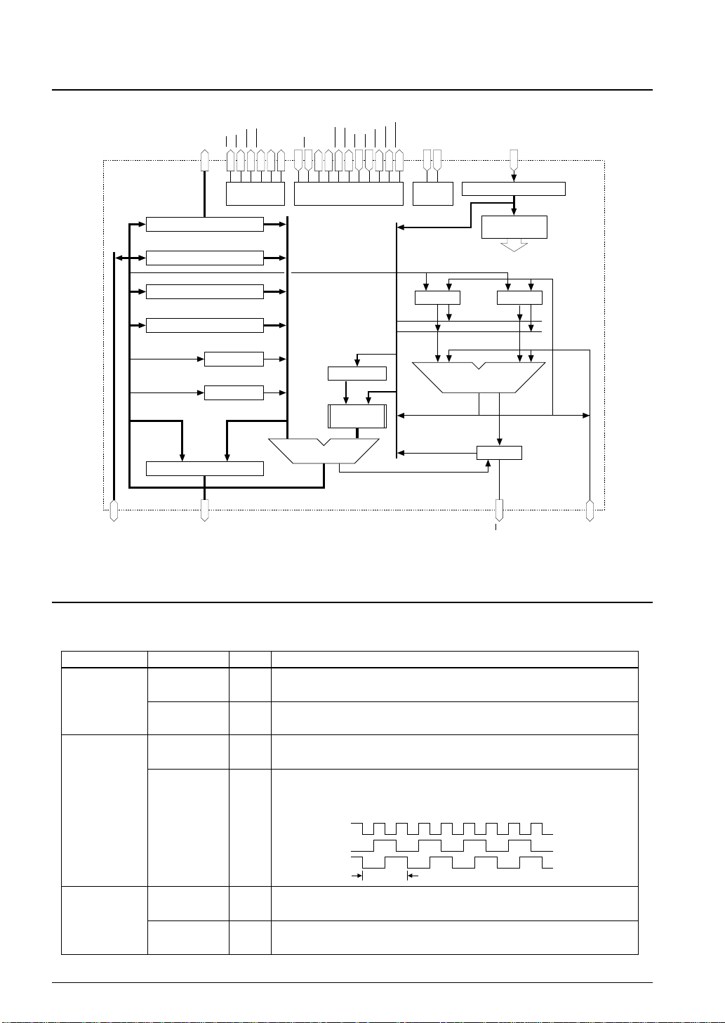
1.3 Block Diagram
Figure 1.3.1 shows the S1C63000 block diagram.
M00
DATA ADDRESS LATCH
–M15
IA00
–IA15
PC (16)
QUEUE (16)
X (16)
Y (16)
SP2 (8)
SP1 (8)
DA00
–DA15
RDWRRDIV
BS16
DBS0
DBS1
BUS
CONTROL
CLKSRPKPLSTOP
TIMING & INTERRUPT
Port A Port B
16-bit ADDER
USLP
CONTROL
EXT (8)
ADDRESS
OPERATOR
IRQ
NMI
IACK
Fig. 1.3.1 S1C63000 block diagram
NACK
SS
FETCH
VDDV
POWER
SUPPLY
A (4)
Port A Port B
S1C63000
INSTRUCTION
4-bit ALU
I00
–I12
IR (13)
DECODER
µ Instruction
B (4)
F (4)
IF
D0
–D3
1.4 Input-Output Signals
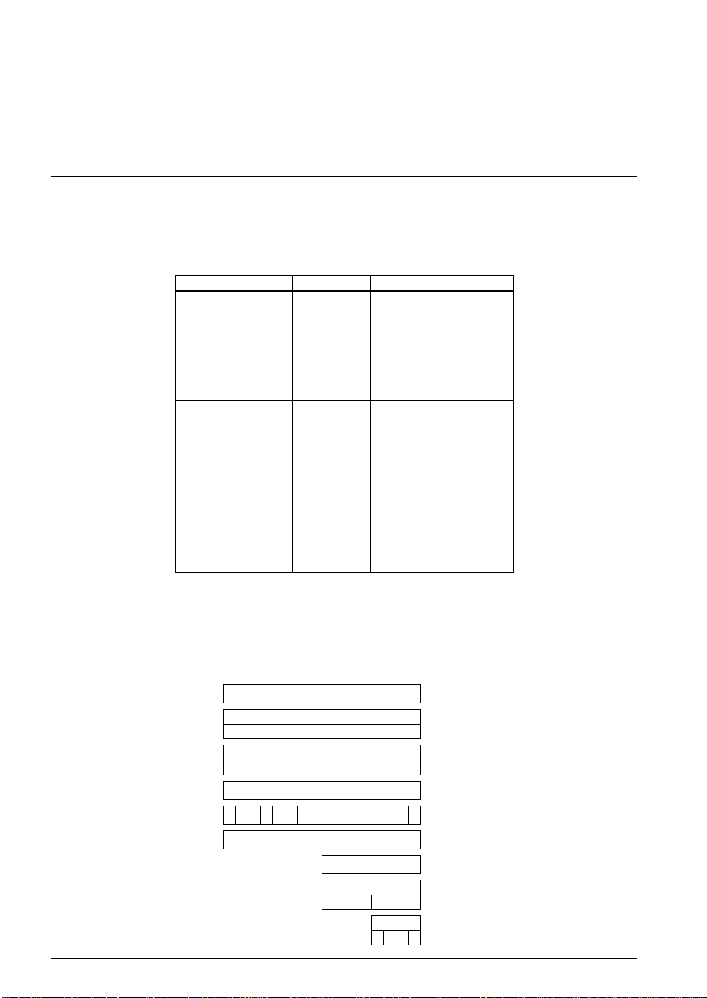
Tables 1.4.1 (a) and 1.4.1 (b) show the input/output signals between the S1C63000 and peripheral circuits.
Table 1.4.1(a) Input/output signal list (1)
Type I/O
Power supply
VDD (VD1)
Power supply (+)
I
Inputs a plus supply voltage.
VSS (VS1)
Power supply (-)
I
Inputs a minus supply voltage.
Clock
CLK
I
Clock input
Inputs the system clock from the peripheral circuit.
PK
PL
2-phase divided clock output
O
Outputs the 2-phase divided signals to be generated from the system clock
input to the CLK terminal as following phase.
CLK
PK
PL
1 cycle
Address bus
IA00–IA15
Instruction address output
O
Outputs an instruction (code ROM) address.
DA00–DA15
Data address output
O
Outputs a data (RAM, I/O) address.
2 EPSON S1C63000 CORE CPU MANUAL
FunctionTerminal name
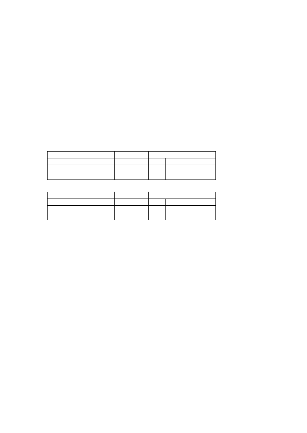
Page 9
Type I/O
Data bus
Bus control
signal
System control
signal
Interrupt signal
Status signal
I00–I12
M00–M15
D0–D3
RD
WR
RDIV
SR
USLP
NMI
IRQ
IACK
NACK
FETCH
STOP
IF
BS16
DBS0
DBS1
CHAPTER 1: OUTLINE
Table 1.4.1(b) Input/output signal list (2)
FunctionTerminal name
I
Instruction bus
Inputs an instruction code.
I/O
16-bit data bus
A bidirectional data bus to connect to the RAM (stack RAM) for 16-bit accessing.
I/O
4-bit data bus
A bidirectional data bus to connect to the RAM and I/O.
O
Data read
Goes to a low level when the CPU reads data (from RAM, I/O).
O
Data write
Goes to a low level when the CPU writes data (to RAM, I/O).
O
Read interrupt vector
Goes to a low level when the CPU reads an interrupt vector.
I
Reset input
A low level input resets the CPU.
O
Micro sleep
Goes to a low level when the CPU executes the SLP instruction.
The peripheral circuit stops oscillation on the basis of this signal.
I
Non-maskable interrupt request
An interrupt request terminal for an interrupt that cannot be masked by software.
It is accepted at the falling edge of an input signal to this terminal.
I
Interrupt request
An interrupt request terminal for interrupts that can be masked by software.
It is accepted by a low level signal input to this terminal.
O
Interrupt acknowledge
Goes to a low level while executing an NMI or IRQ interrupt response cycle.
O
Non-maskable interrupt acknowledge
Goes to a low level while executing a non-maskable interrupt response cycle.
O
Fetch cycle
Goes to a low level when the CPU fetches an instruction.
O
Stop signal
Goes to a low level when the CPU is in stop status after executing the HALT
or SLP instruction, or in reset status (SR is low).
O
Interrupt flag
Outputs a status (inverted value) of the interrupt flag in the flag (F) register.
O
16-bit access
Goes to a low level when the CPU accesses to a 16-bit RAM.
O
Data bus status
Outputs data bus status (for both the 4-bit and 16-bit data bus).
DBS1
DBS0
State
0
0
High impedance
0
1
Interrupt vector read
1
0
Memory write
1
1
Memory read
See Chapter 3, "CPU OPERATION", for the timing of the signals.
S1C63000 CORE CPU MANUAL EPSON 3
Page 10
CHAPTER 2: ARCHITECTURE
CHAPTER 2ARCHITECTURE
This chapter explains the S1C63000 ALU, registers, configuration of the program memory area and
data memory area, and addressing.
2.1 ALU and Registers
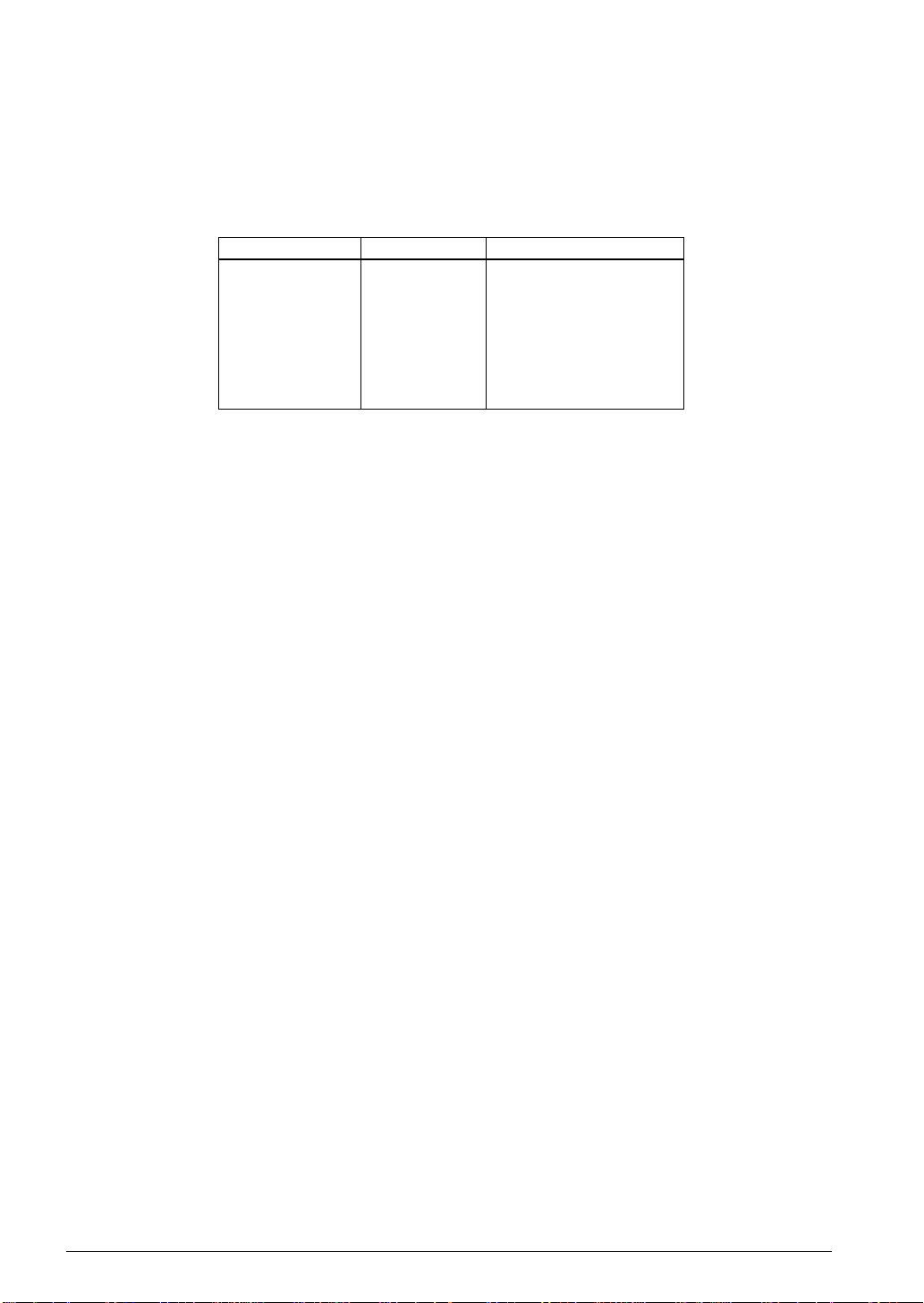
2.1.1 ALU
The ALU (Arithmetic and Logic Unit) loads 4-bit data from a memory or a register and operates the data
according to the instruction. Table 2.1.1.1 shows the ALU operation functions.
Table 2.1.1.1 ALU operation functions
Function classification
Arithmetic
Logic
Rotate / shift
Mnemonic Operation
ADD
ADC
SUB
SBC
CMP
INC
DEC
AND
OR
XOR
BIT
CLR
SET
TST
RL
RR
SLL
SRL
Addition
Addition with carry
Subtraction
Subtraction with carry
Comparison
Increment (adds 1)
Decrement (subtracts 1)
Logical product
Logical sum
Exclusive OR
Bit test
Bit clear
Bit set
Bit test
Rotate to left with carry
Rotate to right with carry
Logical shift to left
Logical shift to right
The operation result is stored to a register or memory according to the instruction.
In addition, the Z (zero) flag and C (carry) flag are set/reset according to the operation result.
2.1.2 Register configuration
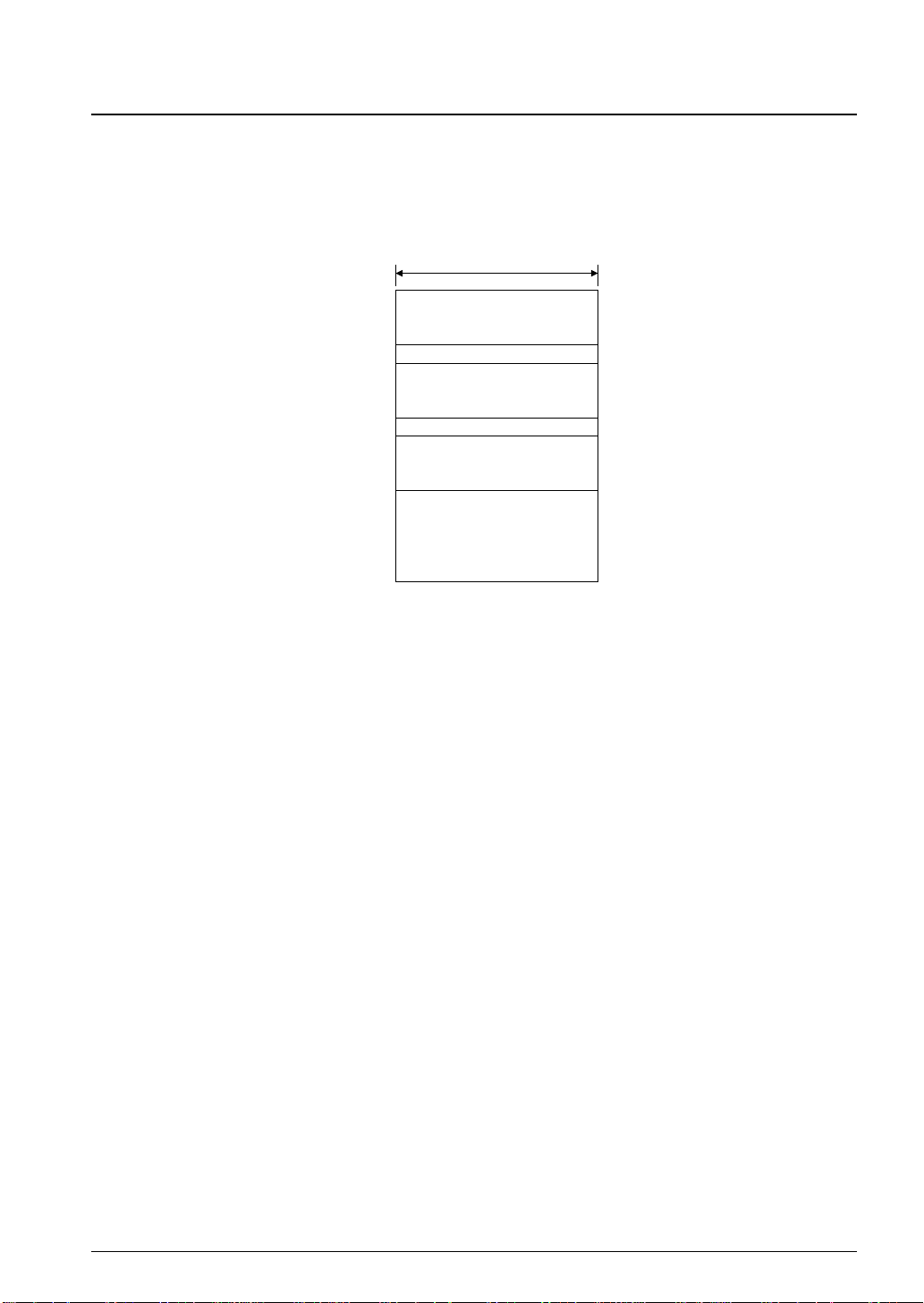
Figure 2.1.2.1 shows the register configuration of the S1C63000.
15 0
15 0
XH
70
15 0
YH
70
15 0
00H
Fig. 2.1.2.1 Register configuration
4 EPSON S1C63000 CORE CPU MANUAL
PC
X
07
XL
Y
07
YL
QUEUE
SP1
7
7
7
70
B
30
0
SP2
EXT
BA
03
30
Program counter
Index register X
Index register Y
Queue register
Stack pointer 1
00000000
Stack pointer 2
0
Extension register
0
Data register B & A
A
F
Flag register
ZCIE
Page 11

CHAPTER 2: ARCHITECTURE
• A and B registers
The A and B registers are respective 4-bit data registers that are used for data transfer and operation
with other registers, data memories or immediate data. They are used independently for 4-bit trans-
fer/operations and used in a BA pair that makes the B register the high-order 4 bits for 8-bit transfer/
operations.
• X and Y registers
The X and Y registers are respective 16-bit index registers that are used for indirect addressing of the
data memory. These registers are configured as an 8-bit register pair (high-order 8 bits: XH/YH, low-
order 8 bits: XL/YL) and data transfer/operations can be done in an 8-bit unit or a 16-bit unit.
• PC (program counter)
The PC is a 16-bit counter to address a program memory and indicates the following address to be
executed.
• SP1 and SP2 (stack pointers)
The SP1 and SP2 are respective 8-bit registers that indicate a stack address in the data memory. 8 bits
of the SP1 correspond to the DA02 to DA09 bits of the address bus for 16-bit data accessing (address
stacking) and it is used to operate the stack in a 4-word (16-bit) unit. 8 bits of the SP2 correspond to
the low-order 8 bits (DA01 to DA07) of the address bus for 4-bit data accessing and it is used to
operate stack in 1-word (4-bit) unit.
See Section 2.3.3, "Stack and stack pointer" for details of the stack operation.
• EXT register
The EXT register is an 8-bit data register that is used when an address or data is extended into 16 bits.
See Section 2.1.5, "EXT register and data extension", for details.
• F register
The F register includes 4 bits of flags; Z and C flags that are changed by operation results, I flag that is
used to enable/disable interrupts, and E flag that indicates extended addressing mode.
• Queue register
The queue register is used as a queue buffer for data when the SP1 processes 16-bit stack operations.
This register is provided in order to process 16-bit data pop operations from the SP1 stack at high-
speed. The queue register is accessed by the hardware, so it is not necessary to be aware of the register
operation when programming.
2.1.3 Flags
The S1C63000 contains a 4-bit flag register (F register) that indicates such things as the operation result
status within the CPU.
30
F
Flag register
ZCIE
Z (zero) flag
C (carry) flag
I (interrupt) flag
E (extension mode) flag
Fig. 2.1.3.1 F (flag) register
• Z (zero) flag
The Z flag is set to "1" when the execution result of an arithmetic instruction or a shift/rotate instruc-
tion has become "0" and is reset to "0'" when the result is other than "0".
Arithmetic instructions that change the Z flag:
ADD, ADC, SUB, SBC, CMP, INC, DEC, AND, OR, XOR, BIT, CLR, SET, TST
S1C63000 CORE CPU MANUAL EPSON 5
Page 12

CHAPTER 2: ARCHITECTURE
Shift/Rotate instructions that change the Z flag:
SLL, SRL, RL, RR
The Z flag is used for condition judgments when executing the conditional jump ("JRZ sign8" and
"JRNZ sign8") instructions, thus it is possible to branch processing to a routine according to the
operation result.
• C (carry) flag
The C flag is set to "1" when a carry (carry from the most significant bit) or a borrow (the most significant bit borrows) has been generated by the execution of an arithmetic instruction and a shift/rotate
instruction, otherwise the flag is set to "0".
Arithmetic instructions that change the C flag:
ADD, ADC, SUB, SBC, CMP, INC, DEC
(It is different from the Z flag, the logic operation instructions except for the instruction that operates
the F register does not change the C flag. In addition, the ADD instructions for the X and Y register
operations and the INC and DEC instructions for the stack pointer operation does not change the C
flag.)
Shift/Rotate instructions that change the C flag:
SLL, SRL, RL, RR
The C flag is used for condition judgments when executing the conditional jump ("JRC sign8" and
"JRNC sign8") instructions, thus it is possible to branch processing to a routine according to the
operation result.
• I flag
The I flag permits and forbids the hardware interrupts except for the NMI. By setting the I flag to "1",
the CPU enters in the EI (enable interrupts) status and the hardware interrupts are enabled. When the
I flag is set to "0", the CPU is in the DI (disable interrupts) and the interrupts except for NMI are
disabled. Furthermore, when a hardware interrupt (including the NMI) is generated, the I flag is reset
to "0" and interrupts after that point are disabled. The multiple interrupts can be accepted by setting
the I flag to "1" in the interrupt processing routine.
The NMI (non-maskable interrupt) is accepted regardless of the I flag setting.
The software interrupts are accepted regardless of the I flag and do not reset the I flag.
The I flag is set to "0" (DI status) at an initial reset, therefore it is necessary to set "1" before using
interrupts by software.
See Section 3.5, "Interrupts" for details.
• E (extension mode) flag
The E flag indicates whether an extended addressing that uses the EXT (extension) register is valid or
invalid. When data is loaded into the EXT register, this flag is set to "1" and the data of the instruction
immediately after that (extended addressable instructions only) is extended with the EXT register.
Then the instruction is executed and the E flag is reset to "0".
See Section 2.1.5, "EXT register and data extension" for details.
• Flag operations
As described above, the flags are automatically set/reset by the hardware. However, it is necessary to
set by software, especially the I flag. The following instructions are provided in order to operate the F
flag.
LD %A,%F Reads all the flag data
LD %F,%A Writes all the flag data
LD %F,imm4 Writes all the flag data
AND %F,imm4 Resets flag(s)
OR %F,imm4 Sets flag(s)
∗ The RETI instruction is used to return from interrupt processing routines (including software
interrupts), and returns the F register data that was evacuated when the interrupt was generated.
XOR %F,imm4 Inverts flag(s)
PUSH %F Evacuates the F register
POP %F Returns the F register
RETI Returns the F register∗
6 EPSON S1C63000 CORE CPU MANUAL
Page 13
CHAPTER 2: ARCHITECTURE
2.1.4 Arithmetic operations with numbering system
In the S1C63000, some instructions support a numbering system. These instructions are indicated with
the following notations in the instruction list.
ADC operand,n4
SBC operand,n4
INC operand,n4
DEC operand,n4
(See "Instruction List" or "Detailed Explanation of Instructions" for the contents of the operand.)
"n4" is a radix, and can be specified from 1 to 16. The additions/subtractions are done in the numbering
system with n4 as the radix. Various counters (such as binary, octal, decimal and hexadecimal) can be
realized easily by software.
The Z flag indicates that an operation result is "0" or not in arithmetics with any numbering system. The
C flag indicates a carry/borrow according to the radix.
The following shows examples of these operation.
Example 1) Octal addition ADC %B,%A,8 (C flag is "0" before operation)
Setting value Result F register
B register A register B register E I C Z
0010B(2) 0111B(7) 0001B(1) 0 – 1 0
0101B(5) 0011B(3) 0000B(0) 0 – 1 1
Example 2) Decimal subtractio SBC %B,%A,10 (C flag is "0" before operation)
Setting value Result F register
B register A register B register E I C Z
1001B(9) 0111B(7) 0010B(2) 0 – 0 0
0001B(1) 0010B(2) 1001B(9) 0 – 1 0
Example 3) 3-digit BCD down counter
LDB %EXT,0 ; Counter base address [0010H]
LD %XL,0x10
LDB [%X]+,0 ; Initial value setting [100]
LDB [%X]+,0
LDB [%X]+,1
:
:
CTDOWN: ; Count down subroutine----------
LDB %EXT,0 ; Counter base address [0010H]
LD %XL,0x10
DEC [%X]+,10 ; Decrements digit 1
SBC [%X]+,0,10 ; Decrements carry from digit 2
SBC [%X],0,10 ; Decrements carry from digit 3
CALR CTDISP ; Count number display routine
LD %A,0 ; Zero check
ADD %A,[%X]
ADD %X,-1
ADD %A,[%X]
ADD %X,-1
JRNZ CTEXIT ; Return if counter is not zero
CALR CTOVER ; Count over processing routine
CTEXIT:
RET
This routine constructs a 3-digit BCD counter using the decimal operation instructions underlined.
Calling the CTDOWN subroutine decrements the counter, and then returns to the main routine. If the
counter has to be zero, the CTOVER subroutine is called before returning to the main routine to
process the end of counting.
S1C63000 CORE CPU MANUAL EPSON 7
Page 14

CHAPTER 2: ARCHITECTURE
• Notes in numbering operations
When performing a numbering operation, set operands in correct notation according to the radix
before operation.
For example, if a decimal operation is done for hexadecimal values (AH to FH), the correct operation
result is not obtained as shown in the following example.
Example: ADC %B,%A,10
Setting value Result F register
B register A register B register E I C Z
1 1001B(9) 1001B(9) 1000B(8) 0 – 1 0 ●●
2 0101B(AH) 1001B(9) 1001B(9) 0 – 1 0 ▲▲
3 1010B(AH) 1010B(AH) 1010B(AH) 0 – 1 0 ×
4 1010B(AH) 1111B(FH) 1111B(FH) 0 – 1 0 ×
Example 1 operates correctly because a decimal value is loaded in the B and A registers.
Examples 3 and 4 do not operate correctly.
Example 2 operates correctly even though it is a wrong setting.
2.1.5 EXT register and data extension
The S1C63000 has a linear 64K-word addressable space, therefore it is required to handle 16-bit address
data. The EXT register and the F flag that extend 8-bit data into 16-bit data permit 16-bit data processing.
The EXT register is an 8-bit register for storing extension data. The E flag indicates that the EXT register
data is valid (extended addressing mode), and is set to "1" by writing data to the EXT register. The E flag
is reset at 1 cycle after setting (during executing the next instruction), therefore an EXT register data is
valid only for the executable instruction immediately after writing. However, that executable instruction
must be a specific instruction which permits the extended addressing to extend the data using the EXT
register. These instructions are specified in "Instruction List" and "Detailed Explanation of Instructions".
Make sure of the instructions when programming.
Note: Do not use instructions (see Instruction List) which are invalid for the extended addressing when
the E flag is set to "1". (Do not use them following instructions that write data to the EXT register or
that set the E flag.) Normal operations cannot be guaranteed if such instructions are used.
(1)Operation for EXT register and E flag (flag register)
The following explains the operation for the EXT register and the E flag (flag register).
• Data setting to the EXT register
The following two instructions are provided to set data in the EXT register.
LDB %EXT,imm8 Loads an 8-bit immediate data to the EXT register
LDB %EXT,%BA Loads the content of the BA register to the EXT register
By executing the instruction, the EXT flag is set to "1" and it indicates that the content of the EXT
register is valid (the content of the EXT register will be used for data extension in the following
instructions).
Furthermore, the content of the EXT register can be read using the instruction below.
LDB %BA,%EXT Loads the content of the EXT register to the BA register
• Setting/resetting the E flag
As mentioned above, the E flag is set to "1" by data setting to the EXT register and reset to "0" while
executing the next instruction.
In addition, the E flag can be set/reset using the following instructions that operate the flags.
LD %F,%A Writes all the flag data
LD %F,imm4 Writes all the flag data
AND %F,imm4 Resets flag(s)
OR %F,imm4 Sets flag(s)
XOR %F,imm4 Inverts flag(s)
8 EPSON S1C63000 CORE CPU MANUAL
Page 15

CHAPTER 2: ARCHITECTURE
The EXT register maintains the data set previously until new data is written or an initial reset. In other
words, the content of the EXT register becomes valid by only setting the E flag using an above instruc-
tion without the register writing and is used for an extended addressing. However, the EXT register is
undefined at an initial reset, therefore, do not directly set the E flag except when the content of the
EXT register has been set for certain.
The following shows the other instructions related to flag data transfer.
LD %A,%F Reads all the flag data
PUSH %F Evacuates the F register
POP %F Returns the F register
RETI Returns the F register ∗
∗ The RETI instruction is used to return from interrupt processing routines (including software inter-
rupts), and returns the F register data that was evacuated when the interrupt was generated.
If an interrupt (including NMI) is generated while fetching an instruction, such as a "LDB %EXT, ••"
instruction or an instruction which writes data to the flag register (the E flag may be set), the interrupt
is accepted after fetching (and executing) the next instruction. In normal processing, data extension
processing is not performed after returning from the interrupt service routine because the interrupt
processing including the F register evacuation is performed after the data extension has finished (E
flag is reset). However, if the stack data in the memory is directly changed in the interrupt service
routine, the F register in which the E flag is set may return. In this case, the instruction immediately
after returning by the RETI instruction is executed in the extended addressing mode by the E flag set
to "1". Pay attention to the F register setting except when consciously describing such a processing. It
is necessary to pay the same attention when returning the F register using the "POP %F" instruction.
(2)Extension with E flag
The following explains the instructions that can be executed when the E flag is set to "1" and its
operation.
• Modifying the indirect addressing with the X and Y registers (for 4-bit data access)
The indirect addressing instructions, which contain [%X] or [%Y] as an operand and accesses 4-bit
data using the X or Y register, functions as an absolute addressing that uses the EXT register data
together with the E flag (= "1").
When an 8-bit immediate data (imm8) is written to the EXT register and the E flag is set immediately
before these instructions, the instruction is modified executing as [%X] = [0000H + imm8] or [%Y] =
[FF00H + imm8]. Therefore, the addressable space with this function is data memory address from
0000H to 00FFH when [%X] is used, and from FF00H to FFFFH when [%Y] is used. Generally, data
that are often used are allocated to the data memory from 0000H to 00FFH and the area from FF00H to
FFFFH is assigned to the I/O memory area (for peripheral circuit control), so these areas are fre-
quently accessed. To access these areas by a normal indirect addressing (if the E flag has not been set)
using the X or Y register, two or three steps of instructions are necessary for setting an address data. In
other words, using this function promotes efficiency of the entire program. See Section 2.3, "Data
Memory" for details of the data memory.
Examples:
LDB %EXT,0x37
LD %A,[%X] ...Works as "LD %A, [0x0037]"
LDB %EXT,0x9C
ADD [%Y],5 ...Works as "ADD [0xFF9C], 5"
Note: This function can be used by only the specific instructions which permits the extended addressing
(see "Instruction List"). Be aware that the operation cannot be guaranteed if the instructions
indicated below are used.
1.Instructions which have a source and /or a destination operand with the post-increment function,
[%X]+ and [%Y]+.
2.Instructions which have [%X] and/or [%Y] in both the source and destination operands.
3.The RETD instruction and the LDB instructions which transfers 8-bit data.
S1C63000 CORE CPU MANUAL EPSON 9
Page 16

CHAPTER 2: ARCHITECTURE
• 16-bit data transfer/arithmetic for the index registers X and Y
The following six instructions, which handle the X or Y register and have an 8-bit immediate data as
the operand, permit the extended addressing.
LDB %XL,imm8 LDB %YL,imm8
ADD %X,sign8 ADD %Y,sign8
CMP %X,imm8 CMP %Y,imm8
When data is written to the EXT register and the E flag is set immediately before these instructions,
the data is processed after extending into 16-bit; imm8 (sign8) is used as the low-order 8 bits and the
content of the EXT register is used as the high-order 8 bits.
Examples:
LDB %EXT,0x15
LDB %XL,0x7D ...Works as "LD %X,0x157D"
LDB %EXT,0xB8
ADD %X,0x4F ...Works as "ADD %X, 0xB84F"
LDB %EXT,0xE6
CMP %X,0xA2 ...Works as "CMP %X, 0x19A2"
∗ 19H = FFH - [EXT] (E6H)
Above examples use the X register, but work the same even when the Y register is used.
Note: The CMP instruction performs a subtraction with a complement, therefore it is necessary to set the
complement (1's complement) of the high-order 8-bit data in the EXT register.
EXT register
←
[FFH - High-order 8-bit data]
• Extending branch addresses
The following PC relative branch instructions, which have a signed 8-bit relative address as the
operand, permit extended addressing.
JR sign8 JRC sign8 JRNC sign8 JRZ sign8 JRNZ sign8
CALR sign8
When data is written to the EXT register and the E flag is set immediately before these instructions,
the relative address is processed after extending into signed 16-bit; sign8 is used as the low-order 8
bits and the content of the EXT register is as the high-order 8 bits.
Examples:
LDB %EXT,0x64
JR 0x29 ...Works as "JR 0x6429"
LDB %EXT,0x00
JR 127 ...Works as "JR 127"
LDB %EXT,0xFF
JR -128 ...Works as "JR -128"
LDB %EXT,0x3A
JR∗ 0x88 ...Works as "JR∗ 0x3A88" (∗ = C, NC, Z, or NZ)
LDB %EXT,0xF8
CALR 0x62 ...Works as "CALR 0xF862"
See Section 2.2.3, "Branch instructions" for the branch instructions.
10 EPSON S1C63000 CORE CPU MANUAL
Page 17
CHAPTER 2: ARCHITECTURE
2.2 Program Memory
2.2.1 Configuration of program memory
The S1C63000 can access a maximum 64K-word (× 13 bits) program memory space. In the individual
model of the S1C63 Family, the ROM of which size is decided depending on the model is connected to
this space to write a program and static data.
Figure 2.2.1.1 shows the program memory map of the S1C63000.
Address
0000H
00FFH
0100H
0101H
010FH
0110H
0111H
013FH
0140H
Program area
Common subroutine, etc.
NMI interrupt vector
Hardware interrupt vectors
Program start address
Software interrupt vectors
Program area
13-bit
FFFFH
Fig. 2.2.1.1 S1C63000 program memory map
The S1C63000 can access 64K-word space linearly without any page management used in current 4-bit
microcomputers.
As shown in Figure 2.2.1.1, the program start address after an initial reset is fixed at 0110H independent
of the S1C63 Family models. Programming should be done so that the execution program starts from that
address.
The address 0100H to 010FH is the hardware interrupt vector's area in which up to 16 interrupt vectors
can be assigned. Address 0100H is for the exclusive use of NMI (non-maskable interrupt). The number of
interrupt vectors is dependent on the interrupt function of the S1C63 Family models. Branch instructions
to the interrupt service routines should be written in this area. See Section 3.5, "Interrupts" for details of
the interrupts.
The address 0111H to 013FH is the software interrupt vector's area. Up to 63 software interrupts can be
set up together with the hardware interrupt vector area. Set branch instructions to the interrupt service
routines in this area similarly to the hardware interrupts.
Addresses from 0000H to 00FFH and from 0140H to FFFFH are program area. A call instruction (CALZ)
that is for the exclusive use of the area from 0000H to 00FFH is provided so that the area is useful to store
common subroutines that are called from relocatable modules.
2.2.2 PC (program counter)
The PC (program counter) is a 16-bit counter that keeps the program address to be executed next. The PC
is incremented by executing every instruction step to execute a program sequentially. When a branch
instruction is executed or an interrupt is generated, the content of the PC is modified to branch the
process flow.
The PC covers the entire program memory space alone, therefore processing such as page management
are unnecessary.
At initial reset, the PC is initialized to 0110H and the program starts executing from that address.
S1C63000 CORE CPU MANUAL EPSON 11
Page 18
CHAPTER 2: ARCHITECTURE
2.2.3 Branch instructions
Various branch instructions are provided for program repeat and subroutine calls that change a sequential program flow controlled with the PC. The branch instruction modifies the PC to branch the program
to an optional address. The types of the branch instructions are classified as follows, according to their
operation differences.
Table 2.2.3.1 Types of branch instructions
Type
PC relative jump
PC relative jump
Indirect jump
Absolute call
PC relative call
Return
Software interrupt
• PC relative jump instructions (JR)
The PC relative jump instruction adds the relative address specified in the operand to the PC that has
indicated the next address, and branches to that address. It permits relocatable programming.
The relative address to be specified in the operand is a displacement from the PC value (address of the
next instruction) when the branch instruction is executed to the branch destination address. When
programming using the S1C63 Family assembler, it is not necessary to calculate displacements
because a branch destination address can be defined as a label and it can be used as an operand.
However, the range of branch destination addresses is different depending on the number of data bits
that are handled as relative addresses.
The following explains the PC relative jump instructions and the relative addresses.
Condition Instruction
Unconditional
Conditional
Unconditional
Unconditional
Unconditional
Unconditional
Unconditional
JR
JRC, JRNC, JRZ, JRNZ
JP
CALZ
CALR
RET, RETS, RETD, RETI
INT
(1) Instructions with a signed 8-bit immediate data sign8 that specifies a relative address
Unconditional jump JR sign8
Conditional jump JRC sign8 JRNC sign8 JRZ sign8 JRNZ sign8
These instructions branch the program sequence with the sign8 specified in the operand as a
signed 8-bit relative address. The range that can be branched is from the next instruction address 128 to +127. A value within the range from -128 to +127 should be used if specifying a value for
jumping in the assembler. Generally branch destination labels such as "JR LABEL" are used, and
they are expanded into the actual address by the assembler.
These instructions permit the extended addressing with the E flag, and the 8-bit relative address
can be extended into 16 bits (the contents of the EXT register become the high-order 8 bits). In this
case, the range that can be branched is from the next instruction address -32768 to +32767. Consequently, in the extended addressing mode these instructions can branch the entire 64K program
memory.
Examples:
JR -100 ...Jumps to the instruction 99 steps before
LDB %EXT,100 ...(100 × 256) = 25600
JR 100 ...Jumps to the instruction 25701 steps after
The unconditional jump instruction "JR sign8" jumps to the branch destination unconditionally
when it is executed.
The conditional jump instructions jump according to the status of C flag or the Z flag.
JRC sign8 ...Jumps if the C flag is "1", or executes the next instruction if the C flag is "0"
JRNC sign8 ...Jumps if the C flag is "0", or executes the next instruction if the C flag is "1"
JRZ sign8 ...Jumps if the Z flag is "1", or executes the next instruction if the Z flag is "0"
JRNZ sign8 ...Jumps if the Z flag is "0", or executes the next instruction if the Z flag is "1"
12 EPSON S1C63000 CORE CPU MANUAL
Page 19

CHAPTER 2: ARCHITECTURE
(2) Instruction with a 4-bit A register data that specifies a relative address
JR %A
This instruction branches the program sequence with the content of the A register as an unsigned
4-bit relative address. The range that can be branched is from the next instruction address +0 to
+15 (absolute value in the A register). This instruction is useful when operation results are used as
the 4-bit relative addresses.
Example:
LD %A,4
JR %A ...Jumps to the instruction 5 steps after
(3) Instruction with an 8-bit BA register data that specifies a relative address
JR %BA
This instruction branches the program sequence with the content of the BA register as an unsigned
8-bit relative address ( the B register data becomes the high-order 4 bits). The range that can be
branched is from the next instruction address +0 to +255 (absolute value in the BA register). This
instruction is useful when operation results are used as the 8-bit relative addresses.
Example:
LDB %BA,29
JR %BA ...Jumps to the instruction 30 steps after
(4) Instruction with a data memory address within 0000H to 003FH in which the content specifies a 4-bit
relative address
JR [addr6]
This instruction branches the program sequence with the content of the data memory specified by
the [addr6] as an unsigned 4-bit relative address. The operand [addr6] can specify a data memory
address within 0000H to 003FH. The range that can be branched is from the next instruction
address +0 to +15 (absolute value in the specified data memory). For the data memory area that is
specified with [addr6], bit operation instructions (CLR, SET, TST) are provided so that various
flags can be set simply. This jump instruction can be used as a conditional jump according to these
flags.
Example: When the content of the address 0010H is 4 (0100B).
SET [0x0010],0 ...Sets the bit 0 in the address 0010H to "1" ([0010H] = 5)
JR [0x0010] ...Jumps to the instruction 6 steps after
• Indirect jump instruction (JP)
The indirect jump instruction "JP %Y" loads the content of the Y register into the PC to branch to that
address unconditionally. This instruction can branch entire 64K program memory because the 16-bit
data in the Y register becomes a branch destination address as it is.
Example:
LDB %EXT,0x24
LDB %YL,0x00 ...Y = 2400H
JP %Y ...Jumps to the address 2400H
Figure 2.2.3.1 shows the operation of the jump instructions and the branch range.
S1C63000 CORE CPU MANUAL EPSON 13
Page 20
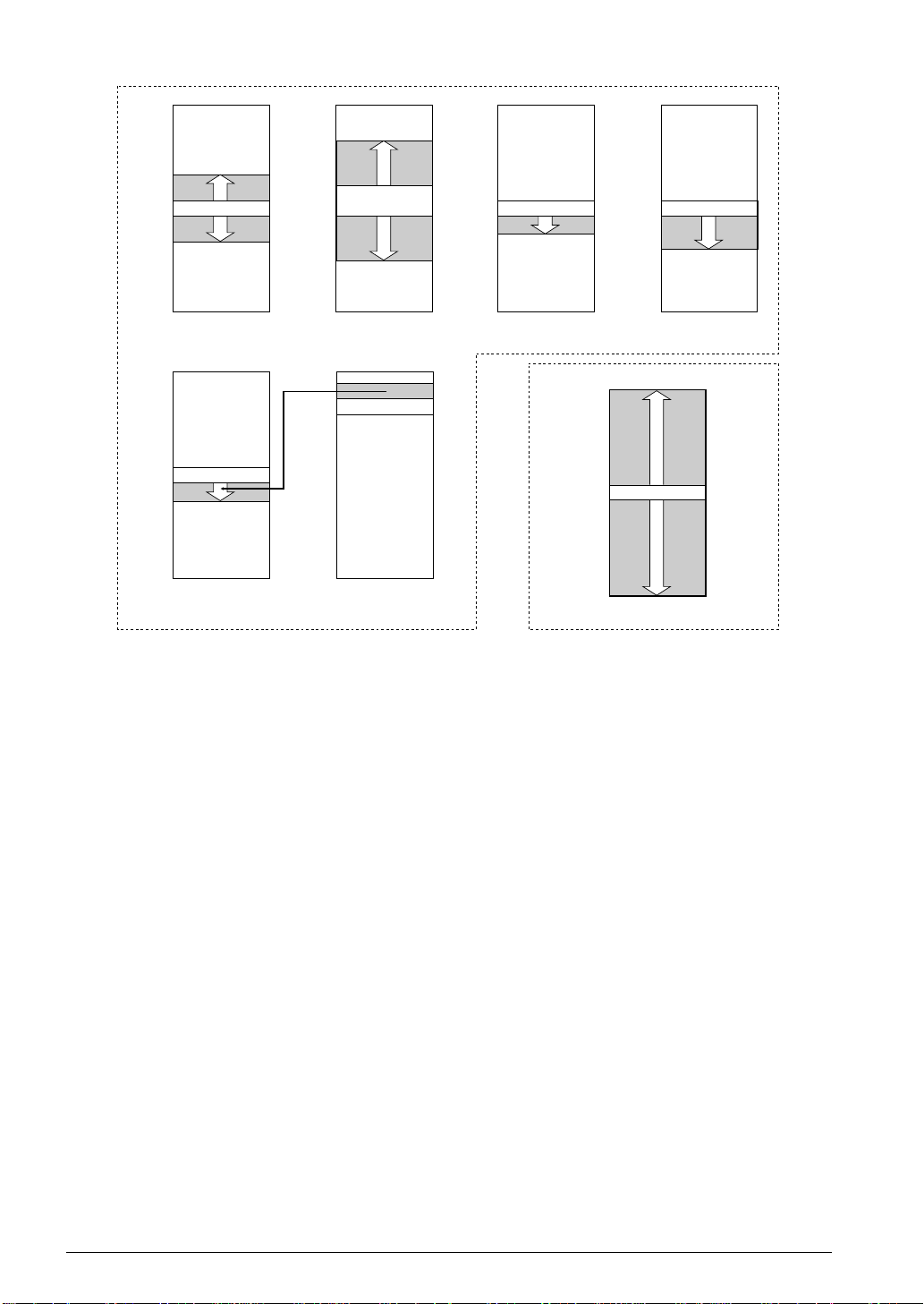
CHAPTER 2: ARCHITECTURE
0000H
xxxxH-127
xxxxH
xxxxH+128
FFFFH
0000H
xxxxH
xxxxH+16
FFFFH
Program memory
Program memory Program memory Program memory
0000H
∗
xxxxH-32767
xxxxH-1
JR sign8
xxxxH+32768
LDB %EXT,imm8
xxxxH
JR sign8
∗
FFFFH
∗ In the extended addressing mode,
this instruction can branch the
entire 64K program memory.
Program memory Data memory
JR [addr6]
[addr6]=0 → xxxxH+1
:
[addr6]=15 → xxxxH+16
PC relative jump instructions
Fig. 2.2.3.1 Operation of jump instructions
xxxxH+16
0000H
addr6
003FH
FFFFH
0000H
xxxxH
FFFFH
JR %A
A=0 → xxxxH+1
:
A=15 → xxxxH+16
0000H
xxxxH
xxxxH+256
FFFFH
Program memory
0000H
JP %Y
FFFFH
Y → Branch destination
absolute address
Indirect jump instruction
JR %BA
BA=0 → xxxxH+1
:
BA=255 → xxxxH+256
• Absolute call instruction (CALZ)
The absolute call instruction "CALZ imm8" calls a subroutine within addresses 0000H to 00FFH. A
subroutine start address (absolute address) should be specified to imm8. When the call instruction is
executed, the PC value (address of the next instruction) is saved into the stack for return, then it
branches to the specified address.
Generally common subroutines that are called from two or more modules are placed in this area when
the program is developed as multiple modules.
Example:
CALZ 0x50 ...Calls the subroutine located at the address 0050H
See Section 2.3.3, "Stack and stack pointer" for stack.
• PC relative call instructions (CALR)
The PC relative call instruction adds the relative address specified in the operand to the PC that has
indicated the next address, and calls a subroutine started from that address. It permits relocatable
programming.
The relative address to be specified in the operand is same as the PC related jump instruction.
The PC value (address of the next instruction) is saved into the stack before branching.
(1) Instructions with a signed 8-bit immediate data sign8 that specifies a relative address
CALR sign8
This instruction branches the program sequence with the sign8 specified in the operand as a
signed 8-bit relative address. The range that can be branched is from the next instruction address 128 to +127. A value within the range from -128 to +127 should be used if specifying a value for
calling in the assembler. Generally branch destination labels such as "CALR LABEL" are used, and
they are expanded into the actual address by the assembler.
14 EPSON S1C63000 CORE CPU MANUAL
Page 21
CHAPTER 2: ARCHITECTURE
This instruction permits the extended addressing with the E flag, and the 8-bit relative address can
be extended into 16 bits (the contents of the EXT register becomes the high-order 8 bits). In this
case, the range that can be branched is from the next instruction address -32768 to +32767. Consequently, in the extended addressing mode this instruction can call subroutines over a 64K program
memory.
Examples:
CALR -50 ...Calls the subroutine 49 steps before
LDB %EXT,50 ...(50 × 256) = 17800
CALR 50 ...Calls the subroutine 17851 steps after
(2) Instruction with a data memory address within 0000H to 003FH in which the content specifies a 4-bit
relative address
CALR [addr6]
This instruction branches the program sequence with the content of the data memory specified by
the [addr6] as an unsigned 4-bit relative address. The operand [addr6] can specify a data memory
address within 0000H to 003FH. The range that can be branched is from the next instruction
address +0 to +15. Same with the "JR [addr6]", this call instruction can be used as a conditional
call according to the flags that are set in the memory specified with [addr6].
Example: When the content of the address 0010H is 4 (0100B).
SET [0x0010],0 ...Sets the bit 0 in the address 0010H to "1" ([0010H] = 5)
CALR [0x0010] ...Calls the subroutine 6 steps after
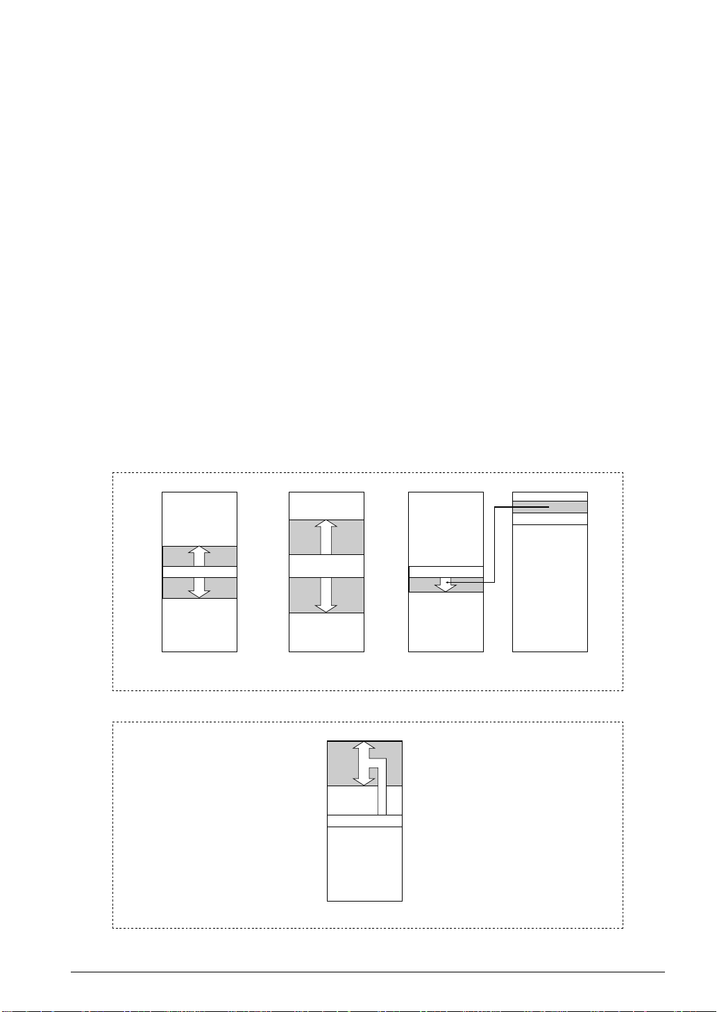
Figure 2.2.3.2 shows the operation of the call instructions and the branch range.
0000H
xxxxH-127
xxxxH
xxxxH+128
FFFFH
Program memory
xxxxH-32767
CALR sign8
xxxxH+32768
Program memory Program memory Data memory
0000H
∗
xxxxH-1
LDB %EXT,imm8
xxxxH
CALR sign8
xxxxH
xxxxH+16
CALR [addr6]
∗
FFFFH
∗ In the extended addressing mode,
this instruction can call subroutines
over a 64K program memory.
FFFFH
[addr6]=0 → xxxxH+1
:
[addr6]=15 → xxxxH+16
PC relative call instructions
Program memory
0000H
00FFH
CALZ imm8
0000H
addr6
003FH
FFFFH
FFFFH
imm → Branch destination
absolute address
Absolute call instruction
Fig. 2.2.3.2 Operation of call instructions
S1C63000 CORE CPU MANUAL EPSON 15
Page 22
CHAPTER 2: ARCHITECTURE
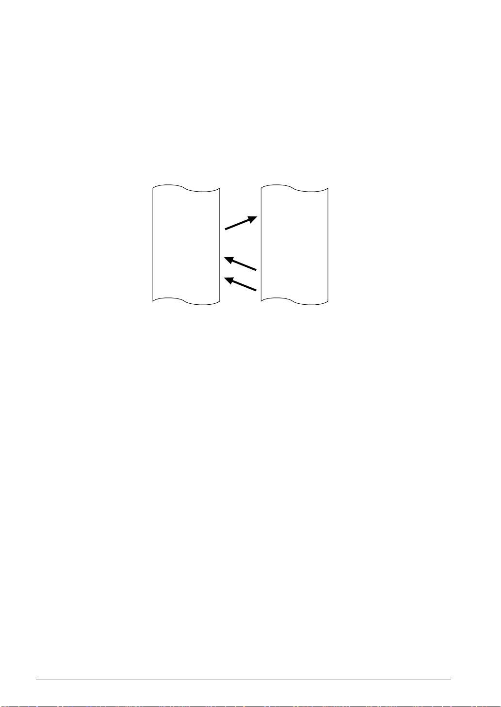
• Return instructions (RET, RETS, RETD, RETI)
A return instruction is used to return from a subroutine called by the call instruction to the routine
that called the subroutine. Return operation is done by loading the PC value (address next to the call
instruction) that was stored in the stack when the subroutine was called into the PC.
The RET instruction operates only to return the PC value in the stack, and the processing is continued
from the address next to the call instruction.
The RETS instruction returns the PC value then adds "1" to the PC. It skips executing an instruction
next to the call instruction.
Figure 2.2.3.3 shows return operations from a subroutine.
Mainroutine Subroutine
:
:
Address
xxxxH
xxxxH+1
xxxxH+2 Return to
:
CALR sign8
JR
sign8
LD
%A,[%X]
:
ADD
A,B
:
JR
NC,1
RET (RETD)
RETS
xxxxH+1
Return to
xxxxH+2
Fig. 2.2.3.3 Return from subroutine
The RETD instruction performs the same operation as the RET instruction, then stores the 8-bit data
specified in the operand into the memory specified with the X register. This function is useful to create
data tables that will be explained in the next section.
The RETI instruction is for the exclusive use of hardware and software interrupt service routines.
When an interrupt is generated, the content of the F register is saved into the stack with the current
PC value. The RETI instruction returns them.
• Software interrupt instruction (INT)
The software interrupt instruction "INT imm6" specifies a vector address within the addresses from
0111H to 013FH to execute its interrupt service routine. It can also call a hardware interrupt service
routine because it can specify an address from 0100H. It performs the same operation with the call
instruction, but the F register is also saved into the stack before branching. Consequently, the RETI
instruction must be used for returning from interrupt service routines. See Section 3.5, "Interrupts" for
details of the interrupt.
2.2.4 Table look-up instruction
The RETD instruction, one of the return instructions, has an 8-bit data in the operand, and stores the data
in the memory specified with the X register (the low-order 8 bits are stored in [X] and the high-order 8
bits are stored in [X+1]) immediately after returning.
By using the RETD instruction combined with the "JR %BA" or "JR %A" instructions, an 8-bit data table
for an LCD segment data conversion or similar can simply be constructed in the code ROM.
Example: The following is an example of a table for converting a BCD data (0 to 9) in the A register
into an ASCII code (30H to 39H). The conversion result is stored in the addresses 0040H
(low-order 4 bits) and 0041H (high-order 4 bits).
LD %A,3 ;Sets data to be converted
CALR TOASCII ;Calls converting routine
LDB %BA,[%X]+ ;Loads result from memory to BA register
:
:
16 EPSON S1C63000 CORE CPU MANUAL
Page 23

CHAPTER 2: ARCHITECTURE
TOASCII: ;BCD to ASCII conversion
LDB %EXT,0x00 ;Sets address 0040H
LDB %XL,0x40
JR %A
RETD 0x30 ;"0"
RETD 0x31 ;"1"
RETD 0x32 ;"2"
RETD 0x33 ;"3"
RETD 0x34 ;"4"
RETD 0x35 ;"5"
RETD 0x36 ;"6"
RETD 0x37 ;"7"
RETD 0x38 ;"8"
RETD 0x39 ;"9"
As shown in the example, operation results in the A or BA register can simply be converted into other
formats.
2.3 Data Memory
2.3.1 Configuration of data memory
In addition to the program memory space, the S1C63000 can also access 64K-word (× 4 bits) data memory.
In the individual model of the S1C63 Family, RAM of which size is decided depending on the model and
I/O memory are connected to this space.
Figure 2.3.1.1 shows the data memory map of the S1C63000.
4-bit
Address
0000H
00FFH
0100H
03FFH
0400H
FEFFH
FF00H
FFFFH
Fig. 2.3.1.1 S1C63000 data memory map
The S1C63000 can access 64K-word space linearly without any of the page management commonly used
in current 4-bit microcomputers.
The S1C63000 has a built-in 16-bit data bus for the address stack (SP1), and a RAM that permits 16-bit
data accessing can be connected to the addresses 0000H to 03FFH. The 16-bit accessible area is different
depending on the individual models. That area permits normal 4-bit accessing. Switching between 4-bit
accessing and 16-bit accessing is done according to the instruction by the hardware. A normal 4-bit data
stack (SP2) is assigned within the addresses 0000H to 00FFH.
SP1, SP2 stack area
Data
and
Data
and
SP1 stack area
Data area
I/O memory area
The addresses FF00H to FFFFH are used for an I/O memory area to control the peripheral circuits.
S1C63000 CORE CPU MANUAL EPSON 17
Page 24

CHAPTER 2: ARCHITECTURE
2.3.2 Addressing for data memory
For addressing to access the data memory, the index registers X and Y, and stack pointers SP1 and SP2 are
used. (The next section will explain the stack pointers.)
Index registers X and Y are both 16-bit registers and cover the entire 64K data memory space. The data
memory is accessed by setting an address in the register.
Example:
LDB %EXT,0x00
LDB %XL,0x10 ...Sets 0010H in the X register
LD A,[%X] ...Loads the content of the memory address 0010H into the A register
The indirect addressing with the X or Y register permits use of the post-increment function and processing for continuous addresses can be done efficiently. This function can be used in the instruction with
[%X]+ or [%Y]+ as an operand. [%X]+ indicates that the content of the X register is incremented after end
of transfer or operation, therefore the next address can be accessed without the X register re-setting. It is
the same in case of the Y register.
Example: To copy the 3-word data from the address specified with the X register to the area specified
with the Y register
LD [%Y]+,[%X]+
LD [%Y]+,[%X]+
LD [%Y],[%X]
In addition, the S1C63000 has also provided instructions in order to efficiently access only the area which
is accessed frequently such as the I/O memory and lower addresses.
One of that is the addressing using the EXT register explained in Section 2.1.5.
• Accessing for addresses 0000H to 00FFH
For absolute addressing in this area, the EXT register and an indirect instruction with the X register
([%X]) are used. To access this area, first write an 8-bit low-order address (00H to FFH) in the EXT
register, then execute an indirect addressing instruction with an operand [%X] (only the instruction
that permits the extended addressing). In this case, the content of the X register does not affect the
address to be accessed. Also the content of the X register is not changed.
Example:
LDB %EXT,0x37
LD %A,[%X] ...Works as "LD %A, [0x0037]"
• Accessing for addresses FF00H to FFFFH (I/O memory area)
For absolute addressing in this area, the EXT register and an indirect instruction with the Y register
([%Y]) are used. To access this area, first write an 8-bit low-order address (00H to FFH) in the EXT
register, then execute an indirect addressing instruction with an operand [%Y] (only the instruction
that permits the extended addressing). In this case, the content of the Y register does not affect the
address to be accessed. Also the content of the Y register is not changed.
Example:
LDB %EXT,0x9C
ADD [%Y],5 ...Works as "ADD [0xFF9C], 5"
Note: The extended addressing function using the EXT register is effective only for the instruction
following immediately after writing data to the EXT register or setting the E flag to "1". For that
instruction, do not use instructions other than the instructions that permit the extended addressing.
Operation cannot be guaranteed if used.
In addition to the above functions, some 6-bit addressing instructions are provided to directly access
that area. These instructions have a [addr6] as the operand and can alone directly access the area
0000H to 003FH or FFC0H to FFFFH.
18 EPSON S1C63000 CORE CPU MANUAL
Page 25
CHAPTER 2: ARCHITECTURE
• Accessing for addresses 0000H to 003FH
Data in this area is used for a relative address by the "JR [addr6]" and "CALR [addr6]" explained in
Section 2.2.3. This area is suitable for setting up various flags and counters since the bit operation
instructions (CLR, SET, TST) and increment/decrement instructions (INC, DEC) are provided for
accessing this area.
• Accessing for addresses FFC0H to FFFFH (I/O memory area)
The bit operation instructions (CLR, SET, TST) are provided for accessing this area. Therefore, control
bits in the I/O memory can be operated simply.
Examples:
CLR [0xFFC0],0 ...Clears the D0 bit in the I/O memory address FFC0H to "0"
SET [0xFFD2],3 ...Sets the D3 bit in the I/O memory address FFD2H to "1"
2.3.3 Stack and stack pointer
The stack is a memory that is accessed in the LIFO (Last In, First Out) format and is allocated to the RAM
area of the address 0000H to 03FFH. The stack area can be set from an optional address (toward the lower
address) using the stack pointer.
The S1C63000 contains two stack pointers SP1 and SP2.
(1)Stack pointer SP1
The SP1 is used for the address data stack, and permits 16-bit data accessing.
D0D1D2D9D10D15
0SP17 00000000
Stack pointer 1
8 bits to be modified
Fig. 2.3.3.1 SP1 configuration
As shown in the figure, the D0, D1 and D10–D15 within the 16 bits are fixed at "0". 8 bits of the D2–D9
can be set by software. Furthermore, the hardware also operates for this 8-bit field. Therefore, addressing by the SP1 is done in 4-word units, and a 16-bit address data can be transferred in one
accessing. Since the SP1 performs 16-bit data accessing, this stack area is limited to the 16-bit accessible RAM area even though it is within the addresses 0000H to 03FFH.
This stack is used to evacuate return addresses when the call instructions are executed or the interrupts are generated. It is also used when the 16-bit data in the X or Y register is evacuated using the
PUSH instruction. The return address data is written into the stack as shown in Figure 2.3.3.2.
The SP1 is decremented after the data is evacuated and is incremented when a return instruction is
executed or after returning data by executing the POP instruction.
Program memory
ROM
Address
1234H
1235H
:
CALR sign8
:
Subroutine
:
RET
PC
1235H
PC
1235H
Address
00FFH
00FEH
00FDH
00FCH
00FFH
00FEH
00FDH
00FCH
ROM
Stack (SP1)
5H
3H
2H
1H
5H
3H
2H
1H
SP1
40H
(= Address 100H)
(= Address FCH)
3FH
SP1
40H
(= Address 100H)
(= Address FCH)
3FH
Fig. 2.3.3.2 Address stack operation
S1C63000 CORE CPU MANUAL EPSON 19
Page 26

CHAPTER 2: ARCHITECTURE
The SP1 increment/decrement affects only the 8-bit field shown in Figure 2.3.3.1, and its operation is
performed cyclically. In other words, if the SP1 is decremented by the PUSH instruction or other
conditions when the SP1 is 00H (indicating the memory address 0000H), the SP1 becomes FFH
(indicating the memory address 03FCH). Similarly, if the SP1 is incremented by the POP instruction or
other conditions when the SP1 is FFH (indicating the memory address 03FCH), the SP1 becomes 00H
(indicating the memory address 0000H).
• Queue register
The queue register is provided in order to reduce the process time of the 16-bit data transfer by
the SP1. The queue register retains 16-bit data in the RAM indicated with the SP1. It is accessed
when the following instructions are executed, not by programs directly.
1. When the call instruction or the PUSH instruction is executed, and when an interrupt is generated
When the CALR or CALZ instruction is executed, a software interrupt by the INT instruction is
generated, and a hardware interrupt is generated, the PC value for returning is written in the
memory [SP1-1]. When the "PUSH %X" or "PUSH %Y" instruction is executed, the content of
the X register or Y register is written in the memory [SP1-1]. At this time, the same data which
is written in the memory [SP1-1] is also written to the queue register.
2. When the return instruction or the POP instruction is executed
When the RET, RETS, RETD, RETI, "POP %X" or "POP %Y" instructions are executed, the data
retained in the queue register is returned to the PC, X register or Y register. Since the SP1 is
incremented, the content of the queue register is renewed (it generates a bus cycle to load the
content of the memory [SP1+1] to the queue register).
3. When the "LDB %SP1, %BA", "INC SP1" or "DEC SP1" instructions are executed
When these instructions are executed, the content of the queue register is also renewed (it
generates a bus cycle to load the content of the memory [SP1] to the queue register).
Note: As shown above, the memory content that is indicated by the SP1 is written to the queue register
according to the SP1 changes. Therefore, the queue register is not renewed even if the memory
[SP1] is directly modified when the SP1 is not changed. Be aware that intended return and POP
operations cannot be performed if such an operation is done.
(2)Stack pointer SP2
The SP2 is used for the normal 4-bit data stack.
D0D7D8D15
Stack pointer 2
SP2
00H
7
8 bits to be modified
Fig. 2.3.3.3 SP2 configuration
In the case of the SP1, the D8–D15 within the 16 bits are fixed at "0". 8 bits of the D0–D7 can be set by
software. Furthermore, the hardware also operates for this 8-bit field. The address range that can be
used for the data stack is limited to within 0000H to 00FFH. Data evacuation/return is done in 1-word
units.
This stack is used to evacuate the F register data when an interrupt is generated. It is also used when
the 4-bit register data (A, B, F) is evacuated using the PUSH instruction. The register data is written
into the stack as shown in Figure 2.3.3.4.
The SP2 is decremented after the data is evacuated and is incremented when the data is returned.
0
20 EPSON S1C63000 CORE CPU MANUAL
Page 27
CHAPTER 2: ARCHITECTURE
Program memory
:
PUSH A
:
POP A
A register
6H
A register
6H
Address
004FH
004EH
004FH
004EH
ROM
Stack (SP2)
6H
6H
SP2
50H
4FH
SP2
50H
4FH
Fig. 2.3.3.4 4-bit stack operation
The SP2 increment/decrement affects only the 8-bit field shown in Figure 2.3.3.3, and its operation is
performed cyclically. In other words, if the SP2 is decremented by the PUSH instruction or other
conditions when the SP2 is 00H (indicating the memory address 0000H), the SP2 becomes FFH
(indicating the memory address 00FFH). Similarly, if the SP2 is incremented by the POP instruction or
other conditions when the SP2 is FFH (indicating the memory address 00FFH), the SP2 becomes 00H
(indicating the memory address 0000H).
(3)Notes for using the stack pointer
• The SP1 and SP2 are undefined at an initial reset. Therefore, both the stack pointers must be initialized
by software.
For safety, all the interrupts including NMI are masked until both the SP1 and SP2 are set by software.
Furthermore, if either the SP1 or SP2 is re-set, all the interrupts are masked again until the other is reset. Therefore be sure to set the SP1 and SP2 as a pair.
• The increment/decrement for the SP1 and SP2 is operated cyclically from 0000H to 03FFH (SP1) and
from 0000H to 00FFH (SP2) regardless of the memory capacity/allocation set up in each model.
Control with the program so that the stacks do not cross over the upper/lower limits of the mounted
memory.
• The SP1 must be set in the RAM area that permits 16-bit accessing depending on the model. The SP1
address stack cannot be allocated to other than the 16-bit accessible area even if the address is less
than 03FFH.
• The area management for the SP1 stack, SP2 stack and data RAM should be done by the user. Pay
attention to these areas so that they do not overlap in the same addresses.
2.3.4 Memory mapped I/O
The S1C63 Family contains the S1C63000 as the core CPU and various types of peripheral circuits, such as
input/output ports. The S1C63000 has adopted a memory mapped I/O system for controlling the
peripheral circuits, and the control bits and the registers for exchanging data are arranged in the data
memory area.
The I/O memory for controlling the peripheral circuits is assigned to the area from FF00H to FFFFH, and
is distinguished from RAM and others. However, the accessing method is the same as RAM, so indirect
addressing can be done using the X or Y register. In addition, since the I/O memory is accessed frequently, the exclusive instructions for this area are also provided. (See Section 2.3.2.)
Refer to the manual for the individual model of the S1C63 Family for the I/O memory and the peripheral
circuits.
S1C63000 CORE CPU MANUAL EPSON 21
Page 28
CHAPTER 3: CPU OPERATION
CHAPTER 3 CPU OPERATION
This section explains the CPU operations and the operation timings.
3.1 Timing Generator and Bus Cycle
The S1C63000 has a built-in timing generator. The timing generator of the S1C63000 generates the twophase divided signals PK and PL based on the clock (CLK) input externally (∗) to make states. One state
is a 1/2 cycle of the CLK and the one bus cycle that becomes the instruction execution unit is composed
of four states.
∗ The clock that is input to the S1C63000 is generated by an oscillation circuit provided outside of the
CPU. The S1C63 Family models have a built-in oscillation circuit.
State State State State
T1 T2 T3 T4
CLK
PK
PL
Bus cycle
Fig. 3.1.1 State and bus cycle
The number of cycles which is stated in the instruction list indicates the number of bus cycles.
3.2 Instruction Fetch and Execution
The S1C63000 executes the instructions indicated with the PC (program counter) one by one. That
operation for an instruction is divided into two stages; one is a fetch cycle to read an instruction, and
another is an execution cycle to execute the instruction that has been read.
All the S1C63000 instructions are composed of one step (word), and are fetched in one bus cycle. An
instruction code that is written in the ROM is read out during the fetch cycle and is analyzed by the
instruction decoder. The FETCH signal goes to a low level during that time. In addition, the PC is
incremented at the end of each fetch.
The analyzed instruction is executed from the next bus cycle. The number of execution cycles is shown in
the instruction list and it is one, two or three bus cycles depending on the instruction.
The S1C63000 contains two different buses for the program memory and the data memory. Consequently,
a fetch cycle for the next instruction can be executed to overlap with the last execution cycle, and it
increases the processing speed. In the one-cycle instructions, the next instruction is fetched at the same
time an instruction is executed.
One bus cycle
T1 T2 T3 T4
CLK
ROM address (PC)
FETCH
Fetch cycle
Execution cycle
PC PC+1 PC+2 PC+3
(PC) (PC+1) (PC+2)
inst. 1 inst. 2 inst. 3
inst. 1 inst. 2 inst. 3
ROM address
:
PC
PC+1
PC+2
PC+3
:
one-cycle
instruction
inst. 1 (one-cycle instruction)
inst. 2 (two-cycle instruction)
inst. 3 (three-cycle instruction)
inst. 4 (one-cycle instruction)
two-cycle
instruction
Instruction
:
:
(PC+3)
inst. 4
three-cycle
instruction
Fig. 3.2.1 Fetch cycle and execution cycle
22 EPSON S1C63000 CORE CPU MANUAL
Page 29
CHAPTER 3: CPU OPERATION
3.3 Data Bus (Data Memory) Control
3.3.1 Data bus status
The S1C63000 output the data bus status in each bus cycle externally on the DBS0 and DBS1 signals as a
2-bit status. The peripheral circuits perform the direction control of the bus driver and other controls with
these signals. The data bus statuses indicated by the DBS0 and DBS1 are as shown in Table 3.3.1.1.
Table 3.3.1.1 Data bus status
DBS1
3.3.2 High-impedance control
The data bus goes to a high-impedance during an execution cycle (∗) that accesses only the internal
registers in the CPU. During the bus cycle period, both the read signal RD and write signal WR are fixed
at a high level and a dummy address is output on the address bus.
CLK
DBS0
0
0
1
1
0
High impedance
1
Interrupt vector read
0
Memory write
1
Memory read
T1 T2 T3 T4
State
PK
PL
DA00–DA15
WR
RD
D0–D3
DBS1
DBS0
Dummy address
Bus cycle
Fig. 3.3.2.1 Bus cycle during accessing internal register
∗ Data is output on the data bus only when the stack pointer SP1 is accessed because a data transfer is
performed between the queue register and the data memory. In this case, the data bus status becomes a
memory write or a memory read depending on the instruction that accesses the SP1.
S1C63000 CORE CPU MANUAL EPSON 23
Page 30
CHAPTER 3: CPU OPERATION
3.3.3 Interrupt vector read
When an interrupt is generated, the CPU reads the interrupt vector output to the data bus by the peripheral circuit that has generated the interrupt. The interrupt vector read status indicates this bus cycle. The
peripheral circuit outputs the interrupt vector to the data bus during this status, and the CPU reads the
data between the T2 and T3 states. At this time, the CPU outputs the RDIV signal (for exclusive use of the
interrupt vector read) as a read signal, not the RD signal that is used for normal data memory read. The
address bus outputs a dummy address during this bus cycle. See Section 3.5 for the operation when an
interrupt is generated.
CLK
PK
PL
DA00–DA15
RDIV
WR
RD
D0–D3
DBS1
T1 T2 T3 T4
Dummy address
Interrupt vector
DBS0
Bus cycle
Fig. 3.3.3.1 Bus cycle during reading interrupt vector
3.3.4 Memory write
In an execution cycle that writes data to the data memory, the writing data is output to the data bus
between the T2 and T4 states and the write signal WR is output in the T3 state. The address bus outputs
the target address during this bus cycle.
The S1C63000 contains a 4-bit data bus (D0–D3) and a 16-bit data bus (M00–M15) for an address stacking.
The CPU switches the data bus according to the instruction. The BS16 signal is provided for this switching.
DA00–DA15
CLaK
PK
PL
WR
RD
D0–D3
BS16
DBS1
DBS0
T1 T2 T3 T4
Address
Write data
CLK
PK
PL
DA00–DA15
WR
RD
M00–M15
BS16
DBS1
DBS0
T1 T2 T3 T4
Address
Write data
Bus cycle
Bus cycle
(a) During 4-bit data access (b) During 16-bit data access
Fig. 3.3.4.1 Bus cycle during memory write
24 EPSON S1C63000 CORE CPU MANUAL
Page 31
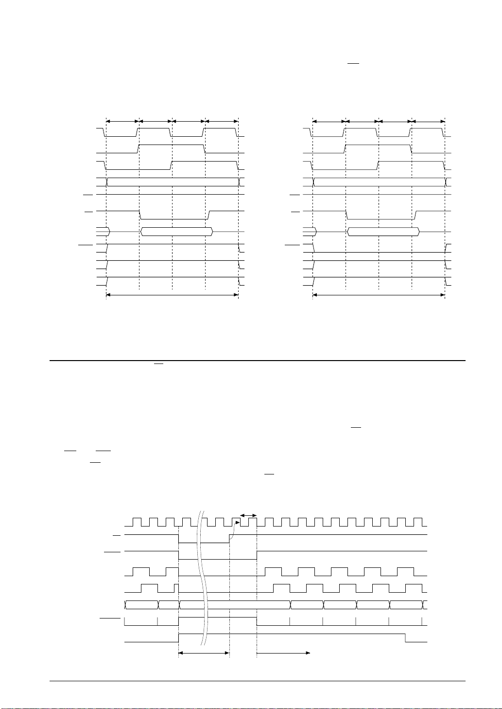
CHAPTER 3: CPU OPERATION
3.3.5 Memory read
In an execution cycle that reads data from the data memory, the read signal RD is output between the T2
and T3 states and data is read from the data bus. The address bus outputs the target address during this
bus cycle.
The 4-bit/16-bit access is the same as the memory write.
CLK
PK
PL
DA00–DA15
WR
RD
D0–D3
BS16
DBS1
DBS0
T1 T2 T3 T4
Address
Read data
CLK
PK
PL
DA00–DA15
WR
RD
M00–M15
BS16
DBS1
DBS0
T1 T2 T3 T4
Address
Read data
Bus cycle
Bus cycle
(a) During 4-bit data access (b) During 16-bit data access
Fig. 3.3.5.1 Bus cycle during memory read
3.4 Initial Reset
The S1C63000 has a reset (SR) terminal in order to start the program after initializing the circuit when the
power is turned on or other situations. The following explains the operation at an initial reset and the
initial setting of the internal registers.
3.4.1 Initial reset sequence
The S1C63000 enters into an initial reset status immediately after setting the SR terminal to a low level,
and the internal circuits are initialized. During an initial reset, the data bus goes to a high-impedance and
the RD and WR signals go to a high level.
When the SR terminal goes to a high level, the initial reset is released and the program starts executing
from address 0110H. The release of an initial reset (the SR terminal goes a high level) is accepted at the
rising edge of the CPU operation clock (CLK), and the first bus cycle ( fetching the instruction of the
address 0110H) starts from 1 clock after.
CLK
SR
STOP
PK
PL
ANY
ANY
ANY
ANY
PC
FETCH
Interrupt mask
110H
1 clock
111H 112H 113H 114H
LDB %BA,imm8 LDB %SP1,%BA LDB %BA,imm8 LDB %SP2,%BA
Interrupt mask
ANY
Reset status Sequence after releasing
Fig. 3.4.1.1 Initial reset status and sequence after releasing
S1C63000 CORE CPU MANUAL EPSON 25
Page 32

CHAPTER 3: CPU OPERATION
After an initial reset, all the interrupts including NMI are masked until both the stack pointers SP1 and
SP2 are set by software.
3.4.2 Initial setting of internal registers
An initial reset initializes the internal registers in the CPU as shown in Table 3.4.2.1.
Table 3.4.2.1 Initial setting of internal registers
Name
Data register A
Data register B
Extension register EXT
Index register X
Index register Y
Program counter
Stack pointer SP1
Stack pointer SP2
Zero flag
Carry flag
Interrupt flag
Extension flag
Queue register
Symbol
A
B
EXT
X
Y
PC
SP1
SP2
Z
C
I
E
Q
Number of bits
4
4
8
16
16
16
8
8
1
1
1
1
16
Setting value
Undefined
Undefined
Undefined
Undefined
Undefined
0110H
Undefined
Undefined
Undefined
Undefined
0
0
Undefined
The registers and flags which are not initialized at an initial reset should be initialized in the program if
necessary.
Be sure to set both the stack pointers SP1 and SP2. All the interrupts cannot be accepted if they are not set
as a pair.
3.5 Interrupts
Interrupt is a function to process factors, that generate asynchronously with program execution, such as a
key entry and an end of a peripheral circuit operation. When the CPU accepts an interrupt request that is
sent by the hardware, the CPU stops executing the current sequence of the program and shifts into the
interrupt processing. When all the interrupt processing has finished, the interrupted program is resumed.
The S1C63000 has the hardware interrupt function for the peripheral circuits including an NMI (nonmaskable interrupt) and the hardware interrupt function. The hardware interrupts excluding the NMI
can be set to the DI (disable interrupts) status by setting the I (interrupt) flag.
I flag = "1": EI (enable interrupts) status ...The CPU accepts interrupt requests from the peripheral
circuits.
I flag = "0": DI (disable interrupts) status ...The CPU does not accept interrupt requests from the periph-
eral circuits. (excluding NMI and software interrupts)
The I flag is set to "0" at an initial reset. Furthermore, all the interrupts including NMI are masked and
cannot be accepted regardless of the I flag setting until both the stack pointers SP1 and SP2 are set in the
program after an initial reset.
3.5.1 Interrupt vectors
Interrupt vectors are provided to execute a interrupt service routine corresponding to the interrupt
generated.
The interrupt vectors are assigned to the following addresses in the ROM.
NMI interrupt vector: 0100H
Hardware interrupt vectors: 0101H to 010FH
Software in t e r r u p t v e c t o r s : 0111H to 013FH
26 EPSON S1C63000 CORE CPU MANUAL
Page 33

CHAPTER 3: CPU OPERATION
Each of the addresses listed above corresponds to an interrupt factor individually. A branch (jump)
instruction to the interrupt service routine should be written to these addresses.
Up to 15 hardware interrupt vectors are available, however, the number of vectors is different depending
on the S1C63 Family models. The addresses, that are not assigned to the hardware interrupt vector within
the addresses 0101H to 010FH, can be used as software interrupt vectors. In addition, since the hardware
interrupt service routines can be executed using the software interrupt, up to 63 software interrupts can
be used (excluding the address 0110H because it is the program start address).
3.5.2 Interrupt sequence
• Hardware interrupts
Hardware interrupts including NMI are generated by the peripheral circuits. The peripheral circuit
that contains the interrupt function outputs an interrupt request to the CPU when the interrupt factor
is generated. The NMI terminal for NMI or IRQ terminal for other interrupts goes low. Sampling the
NMI signal is done at the falling edge by the CPU. Sampling the IRQ signal is done at the rising edge
of the T3 state in the bus cycle. The CPU executes the following process after accepting an interrupt
request.
Bus cycle 0 Sampling the interrupt request.
Bus cycle 1 The last execution cycle of the instruction under execution becomes a dummy fetch
cycle. This cycle turns the interrupt acknowledge signal low (both NACK and IACK for
NMI, IACK only for a normal interrupt), which indicates that the interrupt has been
accepted.
Bus cycle 2 Saves the F register into the stack indicated by the SP2, then resets the I flag to "0" to
prohibit following interrupts (excluding NMI).
Bus cycle 3 Sets the data bus status DBS1/DBS0 to "01B". Then, turns the vector read signal RDIV
low and reads the interrupt vector (4 bits) output from the peripheral circuit to the data
bus.
When NMI is generated, this cycle becomes a dummy cycle because the interrupt vector
is fixed at 0100H.
The NACK and/or IACK are returned to high at the end of this cycle.
Bus cycle 4 Fetches the instruction in the interrupt vector (data that is read in Bus cycle 3 becomes
the low-order 4 bits of the vector) and saves the content of the PC (address immediately
after the instruction that is executed in Bus cycle 0 or branch destination address when
it is a branch instruction) to the stack indicated by the SP1.
Bus cycle 5 Executes the instruction fetched in Bus cycle 4. (If it is 1-cycle instruction, the next
instruction is fetched at the same time.)
• Exceptional acceptance of interrupt
For all the interrupts including NMI that are generated during fetching the following instructions
are accepted after the next instruction is fetched (it is executed) even in the EI (enable interrupts)
status.
1. Instructions that set the E flag
LDB %EXT,imm8 LDB %EXT,%BA
2. Instructions that write data in the F (flag) register
LD %F,%A LD %F,imm4 AND %F,imm4 OR %F,imm4
XOR %F,imm4 POP %F RETI
These instructions set the E flag or may set it. Therefore, if an extended addressing instruction
follows them, it is executed previous to the interrupt processing.
Further, these instructions may modify the content of the I flag. If these instructions set the I flag
(EI status), the interrupt processing is done after executing the next instruction. If these instructions reset the I flag (DI status), interrupts generated after the instruction fetch cycle are masked.
S1C63000 CORE CPU MANUAL EPSON 27
Page 34

CHAPTER 3: CPU OPERATION
3. Instructions that set the stack pointer
LDB %SP1,%BA LDB %SP2,%BA
These two instructions are also accepted after fetching the next instruction. However, these
instructions must be executed as a pair. When one of them is fetched at first, all the interrupts
including NMI are masked (interrupts cannot be accepted). Then, when the other instruction is
fetched, that mask is released and interrupts can be accepted after the next instruction is fetched.
CLK
PK
PC
FETCH
BS16
DBS1/0
WR
RD
RDIV
DA00–DA15
D0–D3
M00–M15
NMI
IACK
NACK
PL
pc-2 pc-1 0100H ANY
ANY ANY DUMMY (0100H) ANY
IF
Interrupt sampling
012345
pc
ANY 2 1 2 ANY
DUMMY
SP2-1 DUMMY SP1-1ANY
F reg. ANY
pc
Interrupt processing by the hardware Executing the interrupt service routine
4–6 cycle
Fig. 3.5.2.1 NMI sequence
(normal acceptance)
CLK
PK
PC
FETCH
BS16
DBS1/0
WR
RD
RDIV
DA00–DA15
D0–D3
M00–M15
NMI
IACK
NACK
PL
pc-3 pc-1 0100H ANY
ANY
IF
Interrupt sampling
Interrupt sampling
0 12345
pc-2
LDB %EXT,imm8
ANY
ANY
DUMMY (0100H) ANY
LD %A,[%X]
03
00xxH
[00xxH]
Interrupt processing by the hardware
pc
212ANY
DUMMY
SP2-1 DUMMY SP1-1
F reg. ANY
pc
Executing the interrupt service routine
In this chart, the dummy fetch
cycle starts after fetching the
"LD %A, [%X]" instruction
that follows the "LDB %EXT,
imm8" instruction.
Fig. 3.5.2.2 NMI sequence
(interrupt acceptance
after 1 instruction)
28 EPSON S1C63000 CORE CPU MANUAL
Page 35

CHAPTER 3: CPU OPERATION
CLK
FETCH
BS16
DBS1/0
WR
RD
RDIV
DA00–DA15
D0–D3
M00–M15
IRQ
IACK
NACK
012345
PK
PL
pc-2 pc-1 010xH ANY
PC
ANY ANY DUMMY (010xH) ANY
ANY 2 1 2 ANY
IF
Interrupt sampling
Interrupt processing by the hardware Executing the interrupt service routine
SP2-1 DUMMY SP1-1ANY
4–6 cycle
pc
F reg. xH
Inte rrupt vector
pc
Fig. 3.5.2.3 Hardware interrupt
(IRQ) sequence
(normal acceptance)
CLK
FETCH
BS16
DBS1/0
WR
RD
RDIV
DA00–DA15
D0–D3
M00–M15
IRQ
IACK
NACK
PK
PL
pc-3 pc-1 010xH ANY
PC
ANY
IF
Interrupt sampling
0 12345
pc-2
LDB %EXT,imm8
ANY
ANY
DUMMY (010xH) ANY
LD %A,[%X]
03
00xxH
[00xxH]
Interrupt processing by the hardware Executing the interrupt service routine
pc
212ANY
SP2-1 DUMMY SP1-1
F reg. xH
Inte rrupt vector
pc
In this chart, the dummy fetch
cycle starts after fetching the
"LD %A, [%X]" instruction
that follows the "LDB %EXT,
imm8" instruction.
Fig. 3.5.2.4 Hardware interrupt
(IRQ) sequence
(interrupt acceptance
after 1 instruction)
S1C63000 CORE CPU MANUAL EPSON 29
Page 36

CHAPTER 3: CPU OPERATION
• Software interrupts
The software interrupts are generated by the INT instruction. Time of the interrupt generation is
determined by the software, so the I flag setting does not affect the interrupt. That processing is the
same as the subroutine that evacuates the F register into the stack.
This interrupt does not change the interrupt control signals between the CPU and the peripheral
circuits, or the I flag either. An address that is specified with the operand of the INT instruction is
used as it is as the interrupt vector.
12345
CLK
PK
PL
PC
FETCH
BS16
DBS1/0
WR
RD
RDIV
DA00–DA15
D0–D3
M00–M15
IRQ
IACK
pc-2 pc-1 01addr6H ANY
ANY ANY INT addr6 (01addr6H) ANY
ANY 2 3 2 ANY
IF
pc+1pc
DUMMY
SP2-1 DUMMY SP1-1ANY
F reg. xH
pc+1
Fig. 3.5.2.5 Software interrupt sequence
3.5.3 Notes for interrupt processing
(1) After an initial reset, all the interrupts including NMI are masked and cannot be accepted regardless
of the I flag setting until both the stack pointers SP1 and SP2 are set in the program. Be sure to set the
SP1 and SP2 in the initialize routine.
Further, when re-setting the stack pointer, the SP1 and SP2 must be set as a pair. When one of them is
set, all the interrupts including NMI are masked and interrupts cannot be accepted until the other one
is set.
(2) The interrupt processing is the same as a subroutine call that branches to the interrupt vector address.
At that time, the F register is evacuated into the stack. Therefore, the interrupt service routine should
be made as a subroutine and the RETI instruction that returns the F register must be used for return.
(3) If an interrupt (including NMI) is generated while fetching an instruction, that sets the E flag or writes
data to the F (flag) register, the interrupt is accepted after fetching (and executing) the next instruction. Therefore, the extended addressing with the EXT register is processed before executing the
interrupt processing. However, if the stack data in the memory is directly changed in the interrupt
service routine, the F register in which the E flag is set may return. In this case, the instruction immediately after returning by the RETI instruction is executed in the extended addressing mode by the E
flag that is set to "1". Pay attention to the F register setting except when describing such a processing
consciously.
30 EPSON S1C63000 CORE CPU MANUAL
Page 37

CHAPTER 3: CPU OPERATION
3.6 Standby Status
The S1C63000 has a function that stops the CPU operation and it can greatly reduce power consumption.
This function should be used to stop the CPU when there is no processing to be executed in the CPU,
example while the application program waits an interrupt. This is a standby status where the CPU has
been stopped to shift it to low power consumption.
This status is available in two types, a HALT status and a SLEEP status.
3.6.1 HALT status
The HALT status is the status in which only the CPU stops and shifting to it can be done using the HALT
instruction. The HALT status is released by a hardware interrupt including NMI, and the program
sequence returns to the step immediately after the HALT instruction by the RETI instruction in the
interrupt service routine. The peripheral circuits including the oscillation circuit and timer operate all
through the HALT status. Moreover during HALT status, the contents of the registers in the CPU that
have been set before shifting are maintained.
Figure 3.6.1.1 shows the sequence of shifting to the HALT status and restarting.
In the HALT status the Th1 and Th2 states are continuously inserted. During this period, interrupt
sampling is done at the falling edge of the Th2 state and the generation of an interrupt factor causes it to
shift to the interrupt processing.
Th1
Th1
Th1
Th1
Th1
Th2
Th2
Th1
Th2
T1T2 T3 T4
CLK
T2 T3 T4
T1
Th2
Th2
Th2
PK
PL
PC
FETCH
DBS1/0
STOP
IRQ
IACK
pc
HALT
ANY
HALT status
pc+1
DUMMY
02
Interrupt processing
Interrupt sampling
Fig. 3.6.1.1 Sequence of shifting to HALT status and restarting
3.6.2 SLEEP status
The SLEEP status is the status in which the CPU and the peripheral circuits within the MCU stop operating and shifting it can be done using the SLP instruction.
The SLEEP status is released by a reset or a specific interrupt (it differs depending on the model). When
the SLEEP status is released by a reset, the program restarts from the program start address (0110H).
When it is released by an interrupt, the program sequence returns to the step immediately after the SLP
instruction by the RETI instruction in the interrupt service routine.
Power consumption in the SLEEP status can be greatly reduced in comparison with the the HALT status,
because such peripheral circuits as the oscillation circuit are also stopped. However, since stabilization
time is needed for the oscillation circuit when restarting, it is effective when used for extended standby
where instantaneous restarting is not necessary.
S1C63000 CORE CPU MANUAL EPSON 31
Page 38

CHAPTER 3: CPU OPERATION
During SLEEP status, as in the HALT status, the contents of the registers in the CPU that have been set
before shifting are maintained if rated voltage is supplied.
Figure 3.6.2.1 shows the sequence of shifting to the SLEEP status and restarting.
When an interrupt that releases the SLEEP status is generated, the oscillation circuit begins to oscillate.
When the oscillation starts, the CLK input to the CPU is masked by the peripheral circuit and the input to
the CPU begins after stabilization waiting time (several 10 msec–several msec) has elapsed. The CPU
samples the interrupt at the falling edge of the initially input CLK and starts the interrupt processing.
OSC
CLK
PK
PL
T1
T2 T3 T4
T1T2 T3 T4
PC
FETCH
DBS1/0
STOP
IRQ
pc
SLP
ANY
pc+1
02
Oscillation stable
waiting time
SLEEP status
Fig. 3.6.2.1 Sequence of the shift to SLEEP status and restarting
DUMMY
Interrupt processing
32 EPSON S1C63000 CORE CPU MANUAL
Page 39

CHAPTER 4: INSTRUCTION SET
CHAPTER 4INSTRUCTION SET
The S1C63000 offers high machine cycle efficiency and a high speed instruction set. It has 47 basic
instructions (412 instructions in all) that are designed as an instruction system permitting relocatable
programming.
This chapter explains about the addressing modes for memory management and about the details of each
instruction.
4.1 Addressing Mode
The S1C63000 has the following 8 types of addressing modes and the address specifications corresponding to the various statuses are done concisely and accurately.
• Types of addressing modes
Basic addressing modes (5 types)
1) Immediate data addressing
2) Register direct addressing
3) Register indirect addressing
4) 6-bit absolute addressing
5) Signed 8-bit PC relative addressing
Extended addressing modes (3 types)
1) 16-bit immediate data addressing
2) 8-bit absolute addressing
3) Signed 16-bit PC relative addressing
4.1.1 Basic addressing modes
The basic addressing mode is an addressing function independent of the instruction.
• Immediate data addressing
The immediate data addressing is the addressing mode in which the immediate data is used for
operations and is used as transfer data. Values that are specified in the operand are directly used as
data or addresses. In the instruction list, the following symbols are used to write immediate data.
Table 4.1.1.1 Symbol and size of immediate data
Symbol
imm2
Specifying a bit No. in 4-bit data
imm4
4-bit general-purpose data
imm6
Specifying a software interrupt vector
imm8
8-bit general-purpose data
sign8
Signed 8-bit general-purpose data
n4
Specifying a radix
Examples:
CLR [addr6],imm2 ...Clears a bit specified with imm2 within a 4-bit data in an address [addr6]
LD %A,imm4 ...Loads a 4-bit data imm4 into the A register
INT imm6 ...A software interrupt of which the vector address is specified with imm6
LDB %BA,imm8 ...Loads an 8-bit data imm8 into the BA register
CALZ imm8 ...Calls a subroutine that starts from an address imm8
(Address specifiable range is 0000H to 00FFH.)
ADD %X,sign8 ...Adds a signed 8-bit data sign8 to the X register
ADC %B,%A,n4 ...Adds data in the A register to the B register with a radix n4 specification
Use
Size
2 bits
4 bits
6 bits
8 bits
8 bits
4 bits
Specifiable range
0–3
0–15
0–63
0–255
-128–127
1–16
S1C63000 CORE CPU MANUAL EPSON 33
Page 40

CHAPTER 4: INSTRUCTION SET
• Register direct addressing
The register direct addressing is the addressing mode when specifying a register for the source and/
or destination. Register names should be written with % in front.
Instructions in which the operand has the following register name operate in this addressing mode.
4-bit registers: %A,%B,%F
8-bit registers: %BA,%XH,%XL,%EXT,%SP1,%SP2
16-bit registers: %X,%Y
Examples:
ADD %A,%B ...Adds the data in the B register to the A register
LDB %BA,%XL ...Loads the data in the XL register into the BA register
DEC %SP1 ...Decrements the stack pointer SP1
JR %A ...Jumps using the content of the A register as a relative address
JP %Y ...Jumps to the address indicated with the Y register
• Register indirect addressing
The register indirect addressing is the addressing mode for accessing the data memory and it indirectly specifies the data memory address with the index register X or Y. To write the instructions,
place % in front of the index register name and enclose them with [ ].
Indirect addressing with the X register: Instructions which have [%X] or [%X]+ as the operand
Indirect addressing with the Y register: Instructions which have [%Y] or [%Y]+ as the operand
The content of the X register or Y register regarded as an address, and operations and transfers are
performed for the data stored in the address or the address.
"+" in the [%X]+ and [%Y]+ indicates a post-increment function. Instructions that have these operands
increment the content of the X register or Y register after executing the transfer or operation. This
function is useful to access a continuous addresses in the data memory.
Examples:
SUB %A,[%X] ...Subtracts the content of a memory specified with the X register from the A
register
LD [%X]+,[%Y]+ ...Transfers the content of a memory specified with the Y register to a memory
specified with the X register. Then increments the contents of the X register
and Y register
• 6-bit absolute addressing
The 6-bit absolute addressing is the addressing mode for accessing within the 6-bit address range
from 0000H or FFC0H. Instructions that have [addr6] as the operand operate in this addressing mode.
The address range that can be specified with the addr6 is 0000H to 003FH or FFC0H to FFFFH.
(1) Instructions that access from 0000H to 003FH
For this area, the following instructions, which are used in this area as counters and flags, are
provided. An address within 0000H to 003FH is specified with the addr6.
INC [addr6] ...Increments the content of a memory specified with the addr6
DEC [addr6] ...Decrements the content of a memory specified with the addr6
CLR [addr6],imm2 ...
SET [addr6],imm2 ...Sets a bit specified with the imm2 in a memory specified with the addr6
TST [addr6],imm2 ...Tests a bit
In addition, the following branch instructions, which permit a conditional branch according to the
contents of this area, are provided.
JR [addr6] ...PC relative jump instruction that uses the content of a memory specified
CALR [addr6] ...PC relative call instruction that uses the content of a memory specified with
34 EPSON S1C63000 CORE CPU MANUAL
Clears a bit specified with the imm2 in a memory specified with the addr6
specified with the imm2 in a memory specified with the addr6
with addr6 as a relative address
addr6 as a relative address
Page 41

CHAPTER 4: INSTRUCTION SET
These instructions perform a PC relative branch using the content (4 bits) of a memory specified
with the [addr6] as a relative address. The branch destination address is [the address next to the
branch instruction] + [the contents (0 to 15) of the memory specified with the addr6].
(2) Instructions that access from FFC0H to FFFFH
This area is reserved for the I/O memory in the S1C63 Family and the following instructions are
provided to operate the control bits of the peripheral circuits.
An address within FFC0H to FFFFH is specified with the addr6. However the addr6 is handled as
0 to 3FH in the machine codes.
CLR [addr6],imm2 ...
SET [addr6],imm2 ...Sets a bit specified with the imm2 in a memory specified with the addr6
TST [addr6],imm2 ...
Write only or read only control bits may have been assigned depending on the peripheral circuit.
Pay attention when using the above-mentioned instructions for such bits or addresses containing
such bits.
Clears a bit specified with the imm2 in a memory specified with the addr6
Tests a bit specified with the imm2 in a memory specified with the addr6
• Signed 8-bit PC relative addressing
The signed 8-bit PC relative addressing is the addressing mode used for the branch instructions. The
signed 8-bit relative address (-128 to 127) that is specified in the operand is added to the address next
to the branch instruction to branch to that address.
The following instructions operate in this addressing mode.
Jump instructions: JR sign8
JRC sign8
JRNC sign8
JRZ sign8
JRNZ sign8
Call instruction: CALR sign8
4.1.2 Extended addressing mode
In the S1C63000, when data is written to the EXT register (the E flag is set) and a specific instruction
follows, the data specified by that instruction is extended with the EXT register data (see Section 2.1.5).
When the E flag is set, instructions are extended in an addressing mode different from the mode that is
specified in each instruction. This is the extended addressing mode that will be explained below.
However, instructions that can operate in the extended addressing mode are limited to those indicated in
the instruction list, so check it when programming.
Further the extended addressing mode is effective only for the instruction following immediately after
writing data to the EXT register and setting the E flag to "1" (the E flag is reset to "0" by executing that
instruction). When using an instruction in the extended addressing mode, write data to be extended to
the EXT register or set the E flag (when the E register has already been set).
• 16-bit immediate data addressing
The addressing mode of the following instructions, which have an 8-bit immediate data as the
operand, change to the 16-bit immediate data addressing when the E flag is set to "1". Consequently, it
is possible to transfer and operate a 16-bit immediate data to the X or Y register.
Instructions that operate in the 16-bit immediate data addressing mode with the E flag
LDB %XL,imm8 LDB %Y,imm8
ADD %X,sign8 ADD %Y,sign8
CMP %X,imm8 CMP %X,imm8
The data is extended into 16 bits in which the E register data is the high-order 8 bits and the immediate data specified with the above instruction is the low-order 8 bit.
S1C63000 CORE CPU MANUAL EPSON 35
Page 42

CHAPTER 4: INSTRUCTION SET
Examples:
LDB %EXT,0x15
LDB %XL,0x7D ...Works as "LD %X, 0157D"
LDB %EXT,0xB8
ADD %X,0x4F ...Works as "ADD %X, 0xB84F"
LDB %EXT,0xE6
CMP %X,0xA2 ...Works as "CMP %X, 0x19A2"
∗ 19H = FFH - [EXT] (E6H)
Above examples use the X register, but they work the same even when the Y register is used.
Note: The CMP instruction performs a subtraction with a complement, therefore it is necessary to set the
complement (1’s complement) of the high-order 8-bit data in the EXT register.
EXT register
←
[FFH - High-order 8-bit data]
• 8-bit absolute addressing
The 8-bit absolute addressing is the addressing mode for accessing within the 8-bit address range
from 0000H or FF00H. To enter this mode, write the low-order 8 bits (00H to FFH) of the address to
the EXT register, then execute an indirect addressing instruction which has [%X] or [%Y] as the source
operand or the destination operand. When [%X] is used, the memory from 0000H to 00FFH can be
accessed, and when [%Y] is used, FF00H to FFFFH can be accessed.
Instructions that operate in the 8-bit absolute addressing mode with the E flag
Instruction Operand
LD %r,[%X] %r,[%Y] [%X],%r [%Y],%r [%X],imm4 [%Y],imm4
EX %r,[%X] %r,[%Y]
ADD %r,[%X] %r,[%Y] [%X],%r [%Y],%r [%X],imm4 [%Y],imm4
ADC %r,[%X] %r,[%Y] [%X],%r [%Y],%r [%X],imm4 [%Y],imm4
%B,[%X],n4 %B,[%Y],n4 [%X],%B,n4 [%Y],%B,n4
[%X],0,n4 [%Y],0,n4
SUB %r,[%X] %r,[%Y] [%X],%r [%Y],%r [%X],imm4 [%Y],imm4
SBC %r,[%X] %r,[%Y] [%X],%r [%Y],%r [%X],imm4 [%Y],imm4
%B,[%X],n4 %B,[%Y],n4 [%X],%B,n4 [%Y],%B,n4
[%X],0,n4 [%Y],0,n4
INC [%X],n4 [%Y],n4
DEC [%X],n4 [%Y],n4
CMP %r,[%X] %r,[%Y] [%X],%r [%Y],%r [%X],imm4 [%Y],imm4
AND %r,[%X] %r,[%Y] [%X],%r [%Y],%r [%X],imm4 [%Y],imm4
OR %r,[%X] %r,[%Y] [%X],%r [%Y],%r [%X],imm4 [%Y],imm4
XOR %r,[%X] %r,[%Y] [%X],%r [%Y],%r [%X],imm4 [%Y],imm4
BIT %r,[%X] %r,[%Y] [%X],%r [%Y],%r [%X],imm4 [%Y],imm4
SLL [%X] [%Y]
SRL [%X] [%Y]
RL [%X] [%Y]
RR [%X] [%Y]
∗ "r" indicates the A or B register. Instructions with an operand other than above or the post-incre-
ment function do not have the extended addressing function.
Examples:
LDB %EXT,0x37
LD %A,[%X] ...Works as "LD %A, [0x0037]"
LDB %EXT,0x9C
ADD [%Y],5 ...Works as "ADD [0xFF9C]"
36 EPSON S1C63000 CORE CPU MANUAL
Page 43

CHAPTER 4: INSTRUCTION SET
• Signed 16-bit PC relative addressing
The addressing mode of the following branch instructions, which have an 8-bit relative address as the
operand, change to the signed 16-bit PC relative addressing with the E flag set to "1". Consequently, it
is possible to extend the branch range to the next address -32768 to +32767. (In this mode these
instructions can branch the entire 64K program memory.)
Instructions that operate in the signed 16-bit PC relative addressing mode with the E flag
JR sign8 JRC sign8 JRNC sign8 JRZ sign8 JRNZ sign8
CALR sign8
Examples:
LDB %EXT,0x64
JR 0x29 ...Works as "JR 0x6429"
LDB %EXT,0x3A
JR∗ 0x88 ...Works as "JR∗ 0x3A88" (∗ = C, NC, Z, or NZ)
LDB %EXT,0xF8
CALR 0x62 ...Works as "CALR 0xF862"
4.2 Instruction List
4.2.1 Function classification
Table 4.2.1.1 lists the function classifications of the instructions.
Table 4.2.1.1 Instruction function classifications
Function classification
Arithmetic
Logic
Transfer
Mnemonic Operation
ADD
ADC
SUB
SBC
CMP
INC
DEC
AND
OR
XOR
BIT
CLR
SET
TST
LD
LDB
EX
Addition
Addition with carry
Subtraction
Subtraction with carry
Comparison
Increment (adds 1)
Decrement (subtracts 1)
Logical product
Logical sum
Exclusive OR
Bit test
Bit clear
Bit set
Bit test
Load (4-bit data)
Load (8-bit data)
Exchange (4-bit data)
Function classification
Rotate / shift
Stack control
Branch
System control
Mnemonic Operation
RL
RR
SLL
SRL
PUSH
POP
JR
JP
CALZ
CALR
RET
RETS
RETD
RETI
INT
NOP
HALT
SLP
Rotate to left with carry
Rotate to right with carry
Logical shift to left
Logical shift to right
Push
Pop
Relative jump
Indirect jump
Absolute call
Rrelative call
Return
Return and skip
Return and data set
Interrupt return
Software interrupt
No operation
Shift to HALT status
Shift to SLEEP status
S1C63000 CORE CPU MANUAL EPSON 37
Page 44

CHAPTER 4: INSTRUCTION SET
4.2.2 Symbol meanings
The following indicates the meanings of the symbols used in the instruction list.
Register names
A........................... Data register A (4 bits)
B ........................... Data register B (4 bits)
BA ........................ BA register pair (8 bit s , t h e B regi s t e r i s t h e h i g h - o rder 4 b i t s )
X ........................... Index register X (16 bits)
XH........................ XH register (high-order 8 bits of the X register)
XL......................... XL register (low-order 8 bits of the X register)
Y ........................... Index register Y (16 bits)
YH........................ YH register (high-order 8 bits of the Y register)
YL......................... YL register (low-order 8 bits of the Y register)
F............................ Flag register F (4 bits)
EXT ...................... Extension register EXT (8 bits)
SP1 ....................... Stack pointer SP1 (16 bits, however the setting data is 8 bits of D2 to D9)
SP2 ....................... Stack pointer SP2 (16 bits, however the setting data is 8 bits of D0 to D7)
PC ........................ Program counter PC (16 bits)
In the notation with mnemonics, the register names should be written with a % placed in front of them,
according to the S1C63 Family assembler source format.
%A ....................... A register
%B ........................ B register
%BA..................... BA register
%X........................ X registe r
%XH .................... XH regis t e r
%XL ..................... XL register
%Y........................ Y register
%YH .................... YH regis t e r
%YL ..................... YL register
%F ........................ F register
%EXT................... EXT register
%SP1.................... Stack pointer SP1
%SP2.................... Stack pointer SP2
Immediate data
imm2 ................... 2-bit immediate data (0 to 3)
imm4 ................... 4-bit immediate data (0 to 15)
imm6 ................... Software interrupt vector (0100H to 013FH)
imm8 ................... 8-bit immediate data ( 0 to 255)
i7–i0 ..................... Each bit in immX
n4 ......................... 4-bit radix specification data (1 to 16)
n3–n0 ................... Each bit in n4
sign8 .................... Signed 8-bit immediate data (-128 to 127)
s7–s0 .................... Each bit in sign8
addr6 ................... 6-bit address (00H to 3FH)
a5–a0.................... Each bit in addr6
00addr6 ............... addr6 which specifies an address within 0000H to 003FH
FFaddr6............... addr6 which specifies an address within FFC0H to FFFFH
38 EPSON S1C63000 CORE CPU MANUAL
Page 45

Memory
[%X], [X] ............. Memory where the X register specifies
[%Y], [Y] ............. Memory where the Y register specifies
[00addr6] ............ Memory within 0000H to 003FH where the addr6 specifies
[FFaddr6] ............ Memory within FFC0H to FFFFH where the addr6 specifies
[%SP1], [SP1]...... 16-bit address stack where the SP1 specifies
[%SP2], [SP2]...... 4-bit data stack where the SP2 specifies
Flags
Z ........................... Zero flag
C ...........................Carry fl a g
I ............................ In t e r rup t f l a g
E ...........................Extension flag
↑ ...........................Flag is set
↓ ...........................Flag is reset
↕ ............................Flag is set or reset
–............................Flag is not changed
Operations and others
+ ...........................Addition
- ............................ Subtraction
∧ ...........................Logical product
∨ ...........................Logical sum
∀...........................Exclusive OR
←..........................Data load
↔..........................Data exchange
CHAPTER 4: INSTRUCTION SET
Extended addressing mode (EXT.mode)
●● ..........................Can be u se d
×............................Cannot be used (prohibit use)
S1C63000 CORE CPU MANUAL EPSON 39
Page 46
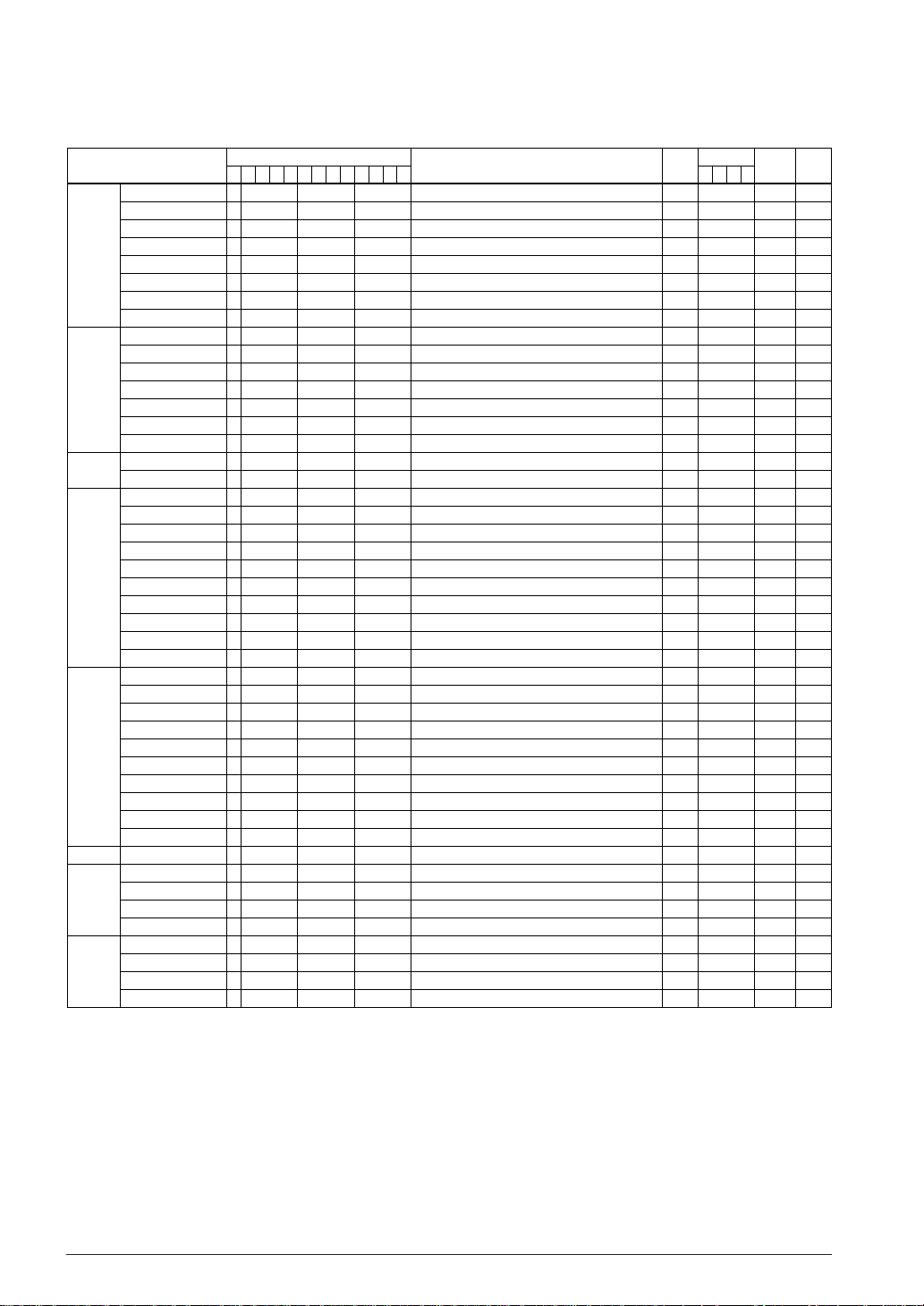
CHAPTER 4: INSTRUCTION SET
4.2.3 Instruction list by function
4-bit data transfer
Mnemonic
LD %A,%A
%A,%B
%A,%F
%A,imm4
%A,[%X]
%A,[%X]+
%A,[%Y]
%A,[%Y]+
LD %B,%A
%B,%B
%B,imm4
%B,[%X]
%B,[%X]+
%B,[%Y]
%B,[%Y]+
LD %F,%A
%F,imm4
LD [%X],%A
[%X],%B
[%X],imm4
[%X],[%Y]
[%X],[%Y]+
[%X]+,%A
[%X]+,%B
[%X]+,imm4
[%X]+,[%Y]
[%X]+,[%Y]+
LD [%Y],%A
[%Y],%B
[%Y],imm4
[%Y],[%X]
[%Y],[%X]+
[%Y]+,%A
[%Y]+,%B
[%Y]+,imm4
[%Y]+,[%X]
[%Y]+,[%X]+
EX %A,%B
EX %A,[%X]
%A,[%X]+
%A,[%Y]
%A,[%Y]+
EX %B,[%X]
%B,[%X]+
%B,[%Y]
%B,[%Y]+
Machine code
12
11109876543210
1111011110000
1111011110010
1111111110110
111101100i3i2i1i0
1111011100000
1111011100001
1111011100010
1111011100011
1111011110100
1111011110110
111101101i3i2i1i0
1111011100100
1111011100101
1111011100110
1111011100111
1111111110101
100001011i3i2i1i0
1111011101000
1111011101100
111101000i3i2i1i0
1111011111010
1111011111011
1111011101001
1111011101101
111101001i3i2i1i0
1111011111110
1111011111111
1111011101010
1111011101110
111101010i3i2i1i0
1111011111000
1111011111001
1111011101011
1111011101111
111101011i3i2i1i0
1111011111100
1111011111101
1111111110111
1000011111000
1000011111001
1000011111010
1000011111011
1000011111100
1000011111101
1000011111110
1000011111111
Operation Cycle Page
A ← A
A ← B
A ← F
A ← imm4
A ← [X]
A ← [X], X ← X+1
A ← [Y]
A ← [Y], Y ← Y+1
B ← A
B ← B
B ← imm4
B ← [X]
B ← [X], X ← X+1
B ← [Y]
B ← [Y], Y ← Y+1
F ← A
F ← imm4
[X] ← A
[X] ← B
[X] ← imm4
[X] ← [Y]
[X] ← [Y], Y ← Y+1
[X] ← A, X ← X+1
[X] ← B, X ← X+1
[X] ← imm4, X ← X+1
[X] ← [Y], X ← X+1
[X] ← [Y], X ← X+1, Y ← Y+1
[Y] ← A
[Y] ← B
[Y] ← imm4
[Y] ← [X]
[Y] ← [X], X ← X+1
[Y] ← A, Y ← Y+1
[Y] ← B, Y ← Y+1
[Y] ← imm4, Y ← Y+1
[Y] ← [X], Y ← Y+1
[Y] ← [X], Y ← Y+1, X ← X+1
A ↔ B
A ↔ [X]
A ↔ [X], X ← X+1
A ↔ [Y]
A ↔ [Y], Y ← Y+1
B ↔ [X]
B ↔ [X], X ← X+1
B ↔ [Y]
B ↔ [Y], Y ← Y+1
Flag EXT.
EICZ
1 ↓ ––– ×
1 ↓ ––– ×
1 ↓ ––– ×
1 ↓ ––– ×
1 ↓ ––– ●
1 ↓ ––– ×
1 ↓ ––– ●
1 ↓ ––– ×
1 ↓ ––– ×
1 ↓ ––– ×
1 ↓ ––– ×
1 ↓ ––– ●
1 ↓ ––– ×
1 ↓ ––– ●
1 ↓ ––– ×
1 ×
1 ×
1 ↓ ––– ●
1 ↓ ––– ●
1 ↓ ––– ●
2 ↓ ––– ×
2 ↓ ––– ×
1 ↓ ––– ×
1 ↓ ––– ×
1 ↓ ––– ×
2 ↓ ––– ×
2 ↓ ––– ×
1 ↓ ––– ●
1 ↓ ––– ●
1 ↓ ––– ●
2 ↓ ––– ×
2 ↓ ––– ×
1 ↓ ––– ×
1 ↓ ––– ×
1 ↓ ––– ×
2 ↓ ––– ×
2 ↓ ––– ×
1 ↓ ––– ×
2 ↓ ––– ●
2 ↓ ––– ×
2 ↓ ––– ●
2 ↓ ––– ×
2 ↓ ––– ●
2 ↓ ––– ×
2 ↓ ––– ●
2 ↓ ––– ×
↔↔↔
↔↔↔
mode
↔
↔
99
99
99
100
100
101
100
101
99
99
100
100
101
100
101
99
100
101
101
102
103
104
102
102
103
104
105
101
101
102
103
104
102
102
103
104
105
90
91
91
91
91
91
91
91
91
40 EPSON S1C63000 CORE CPU MANUAL
Page 47

ALU alithmetic operation (1/3)
Mnemonic
ADD %A,%A
%A,%B
%A,imm4
%A,[%X]
%A,[%X]+
%A,[%Y]
%A,[%Y]+
ADD %B,%A
%B,%B
%B,imm4
%B,[%X]
%B,[%X]+
%B,[%Y]
%B,[%Y]+
ADD [%X],%A
[%X],%B
[%X],imm4
[%X]+,%A
[%X]+,%B
[%X]+,imm4
ADD [%Y],%A
[%Y],%B
[%Y],imm4
[%Y]+,%A
[%Y]+,%B
[%Y]+,imm4
ADC %A,%A
%A,%B
%A,imm4
%A,[%X]
%A,[%X]+
%A,[%Y]
%A,[%Y]+
ADC %B,%A
%B,%B
%B,imm4
%B,[%X]
%B,[%X]+
%B,[%Y]
%B,[%Y]+
ADC [%X],%A
[%X],%B
[%X],imm4
[%X]+,%A
[%X]+,%B
[%X]+,imm4
ADC [%Y],%A
[%Y],%B
[%Y],imm4
[%Y]+,%A
[%Y]+,%B
[%Y]+,imm4
SUB %A,%A
%A,%B
%A,imm4
%A,[%X]
%A,[%X]+
%A,[%Y]
%A,[%Y]+
12
11109876543210
110010111000X
110010111001X
110010100i3i2i1i0
1100101100000
1100101100001
1100101100010
1100101100011
110010111010X
110010111011X
110010101i3i2i1i0
1100101100100
1100101100101
1100101100110
1100101100111
1100101101000
1100101101100
110010000i3i2i1i0
1100101101001
1100101101101
110010001i3i2i1i0
1100101101010
1100101101110
110010010i3i2i1i0
1100101101011
1100101101111
110010011i3i2i1i0
110011111000X
110011111001X
110011100i3i2i1i0
1100111100000
1100111100001
1100111100010
1100111100011
110011111010X
110011111011X
110011101i3i2i1i0
1100111100100
1100111100101
1100111100110
1100111100111
1100111101000
1100111101100
110011000i3i2i1i0
1100111101001
1100111101101
110011001i3i2i1i0
1100111101010
1100111101110
110011010i3i2i1i0
1100111101011
1100111101111
110011011i3i2i1i0
110000111000X
110000111001X
110000100i3i2i1i0
1100001100000
1100001100001
1100001100010
1100001100011
Machine code
Operation Cycle Page
A ← A+A
A ← A+B
A ← A+imm4
A ← A+[X]
A ← A+[X], X ← X+1
A ← A+[Y]
A ← A+[Y], Y ← Y+1
B ← B+A
B ← B+B
B ← B+imm4
B ← B+[X]
B ← B+[X], X ← X+1
B ← B+[Y]
B ← B+[Y], Y ← Y+1
[X] ← [X]+A
[X] ← [X]+B
[X] ← [X]+imm4
[X] ← [X]+A, X ← X+1
[X] ← [X]+B, X ← X+1
[X] ← [X]+imm4, X ← X+1
[Y] ← [Y]+A
[Y] ← [Y]+B
[Y] ← [Y]+imm4
[Y] ← [Y]+A, Y ← Y+1
[Y] ← [Y]+B, Y ← Y+1
[Y] ← [Y]+imm4, Y ← Y+1
A ← A+A+C
A ← A+B+C
A ← A+imm4+C
A ← A+[X]+C
A ← A+[X]+C, X ← X+1
A ← A+[Y]+C
A ← A+[Y]+C, Y ← Y+1
B ← B+A+C
B ← B+B+C
B ← B+imm4+C
B ← B+[X]+C
B ← B+[X]+C, X ← X+1
B ← B+[Y]+C
B ← B+[Y]+C, Y ← Y+1
[X] ← [X]+A+C
[X] ← [X]+B+C
[X] ← [X]+imm4+C
[X] ← [X]+A+C, X ← X+1
[X] ← [X]+B+C, X ← X+1
[X] ← [X]+imm4+C, X ← X+1
[Y] ← [Y]+A+C
[Y] ← [Y]+B+C
[Y] ← [Y]+imm4+C
[Y] ← [Y]+A+C, Y ← Y+1
[Y] ← [Y]+B+C, Y ← Y+1
[Y] ← [Y]+imm4+C, Y ← Y+1
A ← A-A
A ← A-B
A ← A-imm4
A ← A-[X]
A ← A-[X], X ← X+1
A ← A-[Y]
A ← A-[Y], Y ← Y+1
CHAPTER 4: INSTRUCTION SET
Flag EXT.
EICZ
1 ↓ – ×
1 ↓ – ×
1 ↓ – ×
1 ↓ – ●
1 ↓ – ×
1 ↓ – ●
1 ↓ – ×
1 ↓ – ×
1 ↓ – ×
1 ↓ – ×
1 ↓ – ●
1 ↓ – ×
1 ↓ – ●
1 ↓ – ×
2 ↓ – ●
2 ↓ – ●
2 ↓ – ●
2 ↓ – ×
2 ↓ – ×
2 ↓ – ×
2 ↓ – ●
2 ↓ – ●
2 ↓ – ●
2 ↓ – ×
2 ↓ – ×
2 ↓ – ×
1 ↓ – ×
1 ↓ – ×
1 ↓ – ×
1 ↓ – ●
1 ↓ – ×
1 ↓ – ●
1 ↓ – ×
1 ↓ – ×
1 ↓ – ×
1 ↓ – ×
1 ↓ – ●
1 ↓ – ×
1 ↓ – ●
1 ↓ – ×
2 ↓ – ●
2 ↓ – ●
2 ↓ – ●
2 ↓ – ×
2 ↓ – ×
2 ↓ – ×
2 ↓ – ●
2 ↓ – ●
2 ↓ – ●
2 ↓ – ×
2 ↓ – ×
2 ↓ – ×
1 ↓ – ↓↑ ×
1 ↓ – ×
1 ↓ – ×
1 ↓ – ●
1 ↓ – ×
1 ↓ – ●
1 ↓ – ×
mode
↔
↔
↔
↔
↔
↔
↔
↔
↔
↔
↔
↔
↔
↔
↔
↔
↔
↔
↔
↔
↔
↔
↔
↔
↔
↔
↔
↔
↔
↔
↔
↔
↔
↔
↔
↔
↔
↔
↔
↔
↔
↔
↔
↔
↔
↔
↔
↔
↔
↔
↔
↔
↔
↔
↔
↔
↔
↔
↔
↔
↔
↔
↔
↔
↔
↔
↔
↔
↔
↔
↔
↔
↔
↔
↔
↔
↔
↔
↔
↔
↔
↔
↔
↔
↔
↔
↔
↔
↔
↔
↔
↔
↔
↔
↔
↔
↔
↔
↔
↔
↔
↔
↔
↔
68
68
69
69
70
69
70
68
68
69
69
70
69
70
70
70
71
71
71
72
70
70
71
71
71
72
61
61
61
62
62
62
62
61
61
61
62
62
62
62
63
63
64
63
63
64
63
63
64
63
63
64
135
↔
↔
↔
↔
↔
↔
135
↔
135
↔
136
↔
136
↔
136
↔
136
↔
S1C63000 CORE CPU MANUAL EPSON 41
Page 48

CHAPTER 4: INSTRUCTION SET
ALU alithmetic operation (2/3)
Mnemonic
SUB %B,%A
%B,%B
%B,imm4
%B,[%X]
%B,[%X]+
%B,[%Y]
%B,[%Y]+
SUB [%X],%A
[%X],%B
[%X],imm4
[%X]+,%A
[%X]+,%B
[%X]+,imm4
SUB [%Y],%A
[%Y],%B
[%Y],imm4
[%Y]+,%A
[%Y]+,%B
[%Y]+,imm4
SBC %A,%A
%A,%B
%A,imm4
%A,[%X]
%A,[%X]+
%A,[%Y]
%A,[%Y]+
SBC %B,%A
%B,%B
%B,imm4
%B,[%X]
%B,[%X]+
%B,[%Y]
%B,[%Y]+
SBC [%X],%A
[%X],%B
[%X],imm4
[%X]+,%A
[%X]+,%B
[%X]+,imm4
SBC [%Y],%A
[%Y],%B
[%Y],imm4
[%Y]+,%A
[%Y]+,%B
[%Y]+,imm4
CMP %A,%A
%A,%B
%A,imm4
%A,[%X]
%A,[%X]+
%A,[%Y]
%A,[%Y]+
CMP %B,%A
%B,%B
%B,imm4
%B,[%X]
%B,[%X]+
%B,[%Y]
%B,[%Y]+
12
11109876543210
110000111010X
110000111011X
110000101i3i2i1i0
1100001100100
1100001100101
1100001100110
1100001100111
1100001101000
1100001101100
110000000i3i2i1i0
1100001101001
1100001101101
110000001i3i2i1i0
1100001101010
1100001101110
110000010i3i2i1i0
1100001101011
1100001101111
110000011i3i2i1i0
110001111000X
110001111001X
110001100i3i2i1i0
1100011100000
1100011100001
1100011100010
1100011100011
110001111010X
110001111011X
110001101i3i2i1i0
1100011100100
1100011100101
1100011100110
1100011100111
1100011101000
1100011101100
110001000i3i2i1i0
1100011101001
1100011101101
110001001i3i2i1i0
1100011101010
1100011101110
110001010i3i2i1i0
1100011101011
1100011101111
110001011i3i2i1i0
111100111X000
111100111X010
111100100i3i2i1i0
1111001100000
1111001100001
1111001100010
1111001100011
111100111X100
111100111X110
111100101i3i2i1i0
1111001100100
1111001100101
1111001100110
1111001100111
Machine code
Operation Cycle Page
B ← B-A
B ← B-B
B ← B-imm4
B ← B-[X]
B ← B-[X], X ← X+1
B ← B-[Y]
B ← B-[Y], Y ← Y+1
[X] ← [X]-A
[X] ← [X]-B
[X] ← [X]-imm4
[X] ← [X]-A, X ← X+1
[X] ← [X]-B, X ← X+1
[X] ← [X]-imm4, X ← X+1
[Y] ← [Y]-A
[Y] ← [Y]-B
[Y] ← [Y]-imm4
[Y] ← [Y]-A, Y ← Y+1
[Y] ← [Y]-B, Y ← Y+1
[Y] ← [Y]-imm4, Y ← Y+1
A ← A-A-C
A ← A-B-C
A ← A-imm4-C
A ← A-[X]-C
A ← A-[X]-C, X ← X+1
A ← A-[Y]-C
A ← A-[Y]-C, Y ← Y+1
B ← B-A-C
B ← B-B-C
B ← B-imm4-C
B ← B-[X]-C
B ← B-[X]-C, X ← X+1
B ← B-[Y]-C
B ← B-[Y]-C, Y ← Y+1
[X] ← [X]-A-C
[X] ← [X]-B-C
[X] ← [X]-imm4-C
[X] ← [X]-A-C, X ← X+1
[X] ← [X]-B-C, X ← X+1
[X] ← [X]-imm4-C, X ← X+1
[Y] ← [Y]-A-C
[Y] ← [Y]-B-C
[Y] ← [Y]-imm4-C
[Y] ← [Y]-A-C, Y ← Y+1
[Y] ← [Y]-B-C, Y ← Y+1
[Y] ← [Y]-imm4-C, Y ← Y+1
A-A
A-B
A-imm4
A-[X]
A-[X], X ← X+1
A-[Y]
A-[Y], Y ← Y+1
B-A
B-B
B-imm4
B-[X]
B-[X], X ← X+1
B-[Y]
B-[Y], Y ← Y+1
Flag EXT.
EICZ
1 ↓ – ×
mode
↔
↔
1 ↓ – ↓↑ ×
1 ↓ – ×
1 ↓ – ●
1 ↓ – ×
1 ↓ – ●
1 ↓ – ×
2 ↓ – ●
2 ↓ – ●
2 ↓ – ●
2 ↓ – ×
2 ↓ – ×
2 ↓ – ×
2 ↓ – ●
2 ↓ – ●
2 ↓ – ●
2 ↓ – ×
2 ↓ – ×
2 ↓ – ×
1 ↓ – ×
1 ↓ – ×
1 ↓ – ×
1 ↓ – ●
1 ↓ – ×
1 ↓ – ●
1 ↓ – ×
1 ↓ – ×
1 ↓ – ×
1 ↓ – ×
1 ↓ – ●
1 ↓ – ×
1 ↓ – ●
1 ↓ – ×
2 ↓ – ●
2 ↓ – ●
2 ↓ – ●
2 ↓ – ×
2 ↓ – ×
2 ↓ – ×
2 ↓ – ●
2 ↓ – ●
2 ↓ – ●
2 ↓ – ×
2 ↓ – ×
2 ↓ – ×
↔
↔
↔
↔
↔
↔
↔
↔
↔
↔
↔
↔
↔
↔
↔
↔
↔
↔
↔
↔
↔
↔
↔
↔
↔
↔
↔
↔
↔
↔
↔
↔
↔
↔
↔
↔
↔
↔
↔
↔
↔
↔
↔
↔
↔
↔
↔
↔
↔
↔
↔
↔
↔
↔
↔
↔
↔
↔
↔
↔
↔
↔
↔
↔
↔
↔
↔
↔
↔
↔
↔
↔
↔
↔
↔
↔
↔
↔
↔
↔
↔
↔
↔
↔
↔
↔
1 ↓ – ↓↑ ×
1 ↓ – ×
1 ↓ – ×
1 ↓ – ●
1 ↓ – ×
1 ↓ – ●
1 ↓ – ×
1 ↓ – ×
↔
↔
↔
↔
↔
↔
↔
↔
↔
↔
↔
↔
↔
↔
1 ↓ – ↓↑ ×
1 ↓ – ×
1 ↓ – ●
1 ↓ – ×
1 ↓ – ●
1 ↓ – ×
↔
↔
↔
↔
↔
↔
↔
↔
↔
↔
135
135
135
136
136
136
136
137
137
138
137
137
138
137
137
138
137
137
138
123
123
124
124
125
124
125
123
123
124
124
125
124
125
125
125
126
126
126
127
125
125
126
126
126
127
84
84
84
85
85
85
85
84
84
84
85
85
85
85
42 EPSON S1C63000 CORE CPU MANUAL
Page 49

CHAPTER 4: INSTRUCTION SET
ALU alithmetic operation (3/3)
Mnemonic
CMP [%X],%A
[%X],%B
[%X],imm4
[%X]+,%A
[%X]+,%B
[%X]+,imm4
CMP [%Y],%A
[%Y],%B
[%Y],imm4
[%Y]+,%A
[%Y]+,%B
[%Y]+,imm4
INC [00addr6]
DEC [00addr6]
ADC %B,%A,n4
∗1 %B,[%X],n4
%B,[%X]+,n4
%B,[%Y],n4
%B,[%Y]+,n4
ADC [%X],%B,n4
∗1 [%X],0,n4
[%X]+,%B,n4
[%X]+,0,n4
ADC [%Y],%B,n4
∗1 [%Y],0,n4
[%Y]+,%B,n4
[%Y]+,0,n4
SBC %B,%A,n4
∗1 %B,[%X],n4
%B,[%X]+,n4
%B,[%Y],n4
%B,[%Y]+,n4
SBC [%X],%B,n4
∗1 [%X],0,n4
[%X]+,%B,n4
[%X]+,0,n4
SBC [%Y],%B,n4
∗1 [%Y],0,n4
[%Y]+,%B,n4
[%Y]+,0,n4
INC [%X],n4
∗1 [%X]+,n4
INC [%Y],n4
∗1 [%Y]+,n4
DEC [%X],n4
∗1 [%X]+,n4
DEC [%Y],n4
∗1 [%Y]+,n4
"n4" should be specified with a value between 1 and 16 that indicates a radix.
∗1
Machine code
12
11109876543210
1111001101000
1111001101100
111100000i3i2i1i0
1111001101001
1111001101101
111100001i3i2i1i0
1111001101010
1111001101110
111100010i3i2i1i0
1111001101011
1111001101111
111100011i3i2i1i0
1000001
1000000
100001101
111011100
111011101
111011110
111011111
111010100
111010000
111010101
111010001
111010110
111010010
111010111
111010011
100001100
111001100
111001101
111001110
111001111
111000100
111000000
111000101
111000001
111000110
111000010
111000111
111000011
111011000
111011001
111011010
111011011
111001000
111001001
111001010
111001011
a5a4a3a2a1a0
a5a4a3a2a1a0
[ 10H-n4 ]
[ 10H-n4 ]
[ 10H-n4 ]
[ 10H-n4 ]
[ 10H-n4 ]
[ 10H-n4 ]
[ 10H-n4 ]
[ 10H-n4 ]
[ 10H-n4 ]
[ 10H-n4 ]
[ 10H-n4 ]
[ 10H-n4 ]
[ 10H-n4 ]
n3n2n1n0
n3n2n1n0
n3n2n1n0
n3n2n1n0
n3n2n1n0
n3n2n1n0
n3n2n1n0
n3n2n1n0
n3n2n1n0
n3n2n1n0
n3n2n1n0
n3n2n1n0
n3n2n1n0
[ 10H-n4 ]
[ 10H-n4 ]
[ 10H-n4 ]
[ 10H-n4 ]
n3n2n1n0
n3n2n1n0
n3n2n1n0
n3n2n1n0
Operation Cycle Page
[X]-A
[X]-B
[X]-imm4
[X]-A, X ← X+1
[X]-B, X ← X+1
[X]-imm4, X ← X+1
[Y]-A
[Y]-B
[Y]-imm4
[Y]-A, Y ← Y+1
[Y]-B, Y ← Y+1
[Y]-imm4, Y ← Y+1
[00addr6] ← [00addr6]+1
[00addr6] ← [00addr6]-1
B ← N's adjust (B+A+C)
B ← N's adjust (B+[X]+C)
B ← N's adjust (B+[X]+C), X ← X+1
B ← N's adjust (B+[Y]+C)
B ← N's adjust (B+[Y]+C), Y ← Y+1
[X] ← N's adjust ([X]+B+C)
[X] ← N's adjust ([X]+0+C)
[X] ← N's adjust ([X]+B+C), X ← X+1
[X] ← N's adjust ([X]+0+C), X ← X+1
[Y] ← N's adjust ([Y]+B+C)
[Y] ← N's adjust ([Y]+0+C)
[Y] ← N's adjust ([Y]+B+C), Y ← Y+1
[Y] ← N's adjust ([Y]+0+C), Y ← Y+1
B ← N's adjust (B-A-C)
B ← N's adjust (B-[X]-C)
B ← N's adjust (B-[X]-C), X ← X+1
B ← N's adjust (B-[Y]-C)
B ← N's adjust (B-[Y]-C), Y ← Y+1
[X] ← N's adjust ([X]-B-C)
[X] ← N's adjust ([X]-0-C)
[X] ← N's adjust ([X]-B-C), X ← X+1
[X] ← N's adjust ([X]-0-C), X ← X+1
[Y] ← N's adjust ([Y]-B-C)
[Y] ← N's adjust ([Y]-0-C)
[Y] ← N's adjust ([Y]-B-C), Y ← Y+1
[Y] ← N's adjust ([Y]-0-C), Y ← Y+1
[X] ← N's adjust ([X]+1)
[X] ← N's adjust ([X]+1), X ← X+1
[Y] ← N's adjust ([Y]+1)
[Y] ← N's adjust ([Y]+1), Y ← Y+1
[X] ← N's adjust ([X]-1)
[X] ← N's adjust ([X]-1), X ← X+1
[Y] ← N's adjust ([Y]-1)
[Y] ← N's adjust ([Y]-1), Y ← Y+1
In the ADC and INC instructions, the assembler converts the "n4" into a complement, and places it at the low-order 4 bits in
the machine code.
In the SBC and DEC instructions, the "n4" is placed as it is at the low-order 4 bits in the machine code.
(However, when 16 is specified to n4, the machine code is generated with 0000H as the low-order 4 bits.)
Flag EXT.
EICZ
1 ↓ – ●
1 ↓ – ●
1 ↓ – ●
1 ↓ – ×
1 ↓ – ×
1 ↓ – ×
1 ↓ – ●
1 ↓ – ●
1 ↓ – ●
1 ↓ – ×
1 ↓ – ×
1 ↓ – ×
2 ↓ – ×
2 ↓ – ×
2 ↓ – ×
2 ↓ – ●
2 ↓ – ×
2 ↓ – ●
2 ↓ – ×
2 ↓ – ●
2 ↓ – ●
2 ↓ – ×
2 ↓ – ×
2 ↓ – ●
2 ↓ – ●
2 ↓ – ×
2 ↓ – ×
2 ↓ – ×
2 ↓ – ●
2 ↓ – ×
2 ↓ – ●
2 ↓ – ×
2 ↓ – ●
2 ↓ – ●
2 ↓ – ×
2 ↓ – ×
2 ↓ – ●
2 ↓ – ●
2 ↓ – ×
2 ↓ – ×
2 ↓ – ●
2 ↓ – ×
2 ↓ – ●
2 ↓ – ×
2 ↓ – ●
2 ↓ – ×
2 ↓ – ●
2 ↓ – ×
mode
↔
↔
↔
↔
↔
↔
↔
↔
↔
↔
↔
↔
↔
↔
↔
↔
↔
↔
↔
↔
↔
↔
↔
↔
↔
↔
↔
↔
↔
↔
↔
↔
↔
↔
↔
↔
↔
↔
↔
↔
↔
↔
↔
↔
↔
↔
↔
↔
↔
↔
↔
↔
↔
↔
↔
↔
↔
↔
↔
↔
↔
↔
↔
↔
↔
↔
↔
↔
↔
↔
↔
↔
↔
↔
↔
↔
↔
↔
↔
↔
↔
↔
↔
↔
↔
↔
↔
↔
↔
↔
↔
↔
↔
↔
↔
↔
86
86
87
86
86
87
86
86
87
86
86
87
92
88
65
65
66
65
66
66
67
67
68
66
67
67
68
127
128
128
128
128
129
130
129
130
129
130
129
130
93
93
93
93
89
89
89
89
S1C63000 CORE CPU MANUAL EPSON 43
Page 50

CHAPTER 4: INSTRUCTION SET
ALU logic operation (1/2)
Mnemonic
AND %A,%A
%A,%B
%A,imm4
%A,[%X]
%A,[%X]+
%A,[%Y]
%A,[%Y]+
AND %B,%A
%B,%B
%B,imm4
%B,[%X]
%B,[%X]+
%B,[%Y]
%B,[%Y]+
AND %F,imm4
AND [%X],%A
[%X],%B
[%X],imm4
[%X]+,%A
[%X]+,%B
[%X]+,imm4
AND [%Y],%A
[%Y],%B
[%Y],imm4
[%Y]+,%A
[%Y]+,%B
[%Y]+,imm4
OR %A,%A
%A,%B
%A,imm4
%A,[%X]
%A,[%X]+
%A,[%Y]
%A,[%Y]+
OR %B,%A
%B,%B
%B,imm4
%B,[%X]
%B,[%X]+
%B,[%Y]
%B,[%Y]+
OR %F,imm4
OR [%X],%A
[%X],%B
[%X],imm4
[%X]+,%A
[%X]+,%B
[%X]+,imm4
OR [%Y],%A
[%Y],%B
[%Y],imm4
[%Y]+,%A
[%Y]+,%B
[%Y]+,imm4
12
11109876543210
110100111000X
110100111001X
110100100i3i2i1i0
1101001100000
1101001100001
1101001100010
1101001100011
110100111010X
110100111011X
110100101i3i2i1i0
1101001100100
1101001100101
1101001100110
1101001100111
100001000i3i2i1i0
1101001101000
1101001101100
110100000i3i2i1i0
1101001101001
1101001101101
110100001i3i2i1i0
1101001101010
1101001101110
110100010i3i2i1i0
1101001101011
1101001101111
110100011i3i2i1i0
110110111000X
110110111001X
110110100i3i2i1i0
1101101100000
1101101100001
1101101100010
1101101100011
110110111010X
110110111011X
110110101i3i2i1i0
1101101100100
1101101100101
1101101100110
1101101100111
100001001i3i2i1i0
1101101101000
1101101101100
110110000i3i2i1i0
1101101101001
1101101101101
110110001i3i2i1i0
1101101101010
1101101101110
110110010i3i2i1i0
1101101101011
1101101101111
110110011i3i2i1i0
Machine code
A ← A∧A
∧
A ← A
∧
A ← A
A ← A
∧
∧
A ← A
A ← A
∧
∧
A ← A
∧
B ← B
B ← B
∧
∧
B ← B
B ← B
∧
∧
B ← B
∧
B ← B
B ← B
∧
∧
F ← F
[X] ← [X]
[X] ← [X]
[X] ← [X]
[X] ← [X]
[X] ← [X]
[X] ← [X]
[Y] ← [Y]
[Y] ← [Y]
[Y] ← [Y]
[Y] ← [Y]
[Y] ← [Y]
[Y] ← [Y]
∨
A ← A
A ← A
∨
∨
A ← A
∨
A ← A
A ← A
∨
∨
A ← A
A ← A
∨
∨
B ← B
∨
B ← B
B ← B
∨
∨
B ← B
B ← B
∨
∨
B ← B
∨
B ← B
F ← F
∨
[X] ← [X]
[X] ← [X]
[X] ← [X]
[X] ← [X]
[X] ← [X]
[X] ← [X]
[Y] ← [Y]
[Y] ← [Y]
[Y] ← [Y]
[Y] ← [Y]
[Y] ← [Y]
[Y] ← [Y]
Operation Cycle Page
B
imm4
[X]
[X], X ← X+1
[Y]
[Y], Y ← Y+1
A
B
imm4
[X]
[X], X ← X+1
[Y]
[Y], Y ← Y+1
imm4
∧
A
∧
B
∧
imm4
∧
A, X ← X+1
∧
B, X ← X+1
∧
imm4, X ← X+1
∧
A
∧
B
∧
imm4
∧
A, Y ← Y+1
∧
B, Y ← Y+1
∧
imm4, Y ← Y+1
A
B
imm4
[X]
[X], X ← X+1
[Y]
[Y], Y ← Y+1
A
B
imm4
[X]
[X], X ← X+1
[Y]
[Y], Y ← Y+1
imm4
∨
A
∨
B
∨
imm4
∨
A, X ← X+1
∨
B, X ← X+1
∨
imm4, X ← X+1
∨
A
∨
B
∨
imm4
∨
A, Y ← Y+1
∨
B, Y ← Y+1
∨
imm4, Y ← Y+1
EICZ
1 ↓ –– ×
1 ↓ –– ×
1 ↓ –– ×
1 ↓ –– ●
1 ↓ –– ×
1 ↓ –– ●
1 ↓ –– ×
1 ↓ –– ×
1 ↓ –– ×
1 ↓ –– ×
1 ↓ –– ●
1 ↓ –– ×
1 ↓ –– ●
1 ↓ –– ×
1 ↓↓↓↓ ×
2 ↓ –– ●
2 ↓ –– ●
2 ↓ –– ●
2 ↓ –– ×
2 ↓ –– ×
2 ↓ –– ×
2 ↓ –– ●
2 ↓ –– ●
2 ↓ –– ●
2 ↓ –– ×
2 ↓ –– ×
2 ↓ –– ×
1 ↓ –– ×
1 ↓ –– ×
1 ↓ –– ×
1 ↓ –– ●
1 ↓ –– ×
1 ↓ –– ●
1 ↓ –– ×
1 ↓ –– ×
1 ↓ –– ×
1 ↓ –– ×
1 ↓ –– ●
1 ↓ –– ×
1 ↓ –– ●
1 ↓ –– ×
1 ↑↑↑↑ ×
2 ↓ –– ●
2 ↓ –– ●
2 ↓ –– ●
2 ↓ –– ×
2 ↓ –– ×
2 ↓ –– ×
2 ↓ –– ●
2 ↓ –– ●
2 ↓ –– ●
2 ↓ –– ×
2 ↓ –– ×
2 ↓ –– ×
Flag EXT.
mode
↔
↔↔↔↔↔↔↔↔↔↔↔↔↔↔↔↔↔↔↔↔↔↔↔↔↔↔↔↔↔↔↔↔↔↔↔↔↔↔↔↔↔↔↔↔↔↔↔↔↔↔↔
73
73
74
75
75
75
75
73
73
74
75
75
75
75
74
76
76
77
76
76
77
76
76
77
76
76
77
112
112
112
113
114
113
114
112
112
112
113
114
113
114
113
114
114
115
115
115
116
114
114
115
115
115
116
44 EPSON S1C63000 CORE CPU MANUAL
Page 51

ALU logic operation (2/2)
Mnemonic
XOR %A,%A
%A,%B
%A,imm4
%A,[%X]
%A,[%X]+
%A,[%Y]
%A,[%Y]+
XOR %B,%A
%B,%B
%B,imm4
%B,[%X]
%B,[%X]+
%B,[%Y]
%B,[%Y]+
XOR %F,imm4
XOR [%X],%A
[%X],%B
[%X],imm4
[%X]+,%A
[%X]+,%B
[%X]+,imm4
XOR [%Y],%A
[%Y],%B
[%Y],imm4
[%Y]+,%A
[%Y]+,%B
[%Y]+,imm4
BIT %A,%A
%A,%B
%A,imm4
%A,[%X]
%A,[%X]+
%A,[%Y]
%A,[%Y]+
BIT %B,%A
%B,%B
%B,imm4
%B,[%X]
%B,[%X]+
%B,[%Y]
%B,[%Y]+
BIT [%X],%A
[%X],%B
[%X],imm4
[%X]+,%A
[%X]+,%B
[%X]+,imm4
BIT [%Y],%A
[%Y],%B
[%Y],imm4
[%Y]+,%A
[%Y]+,%B
[%Y]+,imm4
CLR [00addr6],imm2
[FFaddr6],imm2
SET [00addr6],imm2
[FFaddr6],imm2
TST [00addr6],imm2
[FFaddr6],imm2
12
110111111000X
110111111001X
110111100i3i2i1i0
1101111100000
1101111100001
1101111100010
1101111100011
110111111010X
110111111011X
110111101i3i2i1i0
1101111100100
1101111100101
1101111100110
1101111100111
100001010i3i2i1i0
1101111101000
1101111101100
110111000i3i2i1i0
1101111101001
1101111101101
110111001i3i2i1i0
1101111101010
1101111101110
110111010i3i2i1i0
1101111101011
1101111101111
110111011i3i2i1i0
110101111000X
110101111001X
110101100i3i2i1i0
1101011100000
1101011100001
1101011100010
1101011100011
110101111010X
110101111011X
110101101i3i2i1i0
1101011100100
1101011100101
1101011100110
1101011100111
1101011101000
1101011101100
110101000i3i2i1i0
1101011101001
1101011101101
110101001i3i2i1i0
1101011101010
1101011101110
110101010i3i2i1i0
1101011101011
1101011101111
110101011i3i2i1i0
10100i1i0
10101i1i0
10110i1i0
10111i1i0
10010i1i0
10011i1i0
Machine code
11109876543210
A ← A∀A
A ← A∀B
A ← A∀imm4
A ← A∀[X]
A ← A∀[X], X ← X+1
A ← A∀[Y]
A ← A∀[Y], Y ← Y+1
B ← B∀A
B ← B∀B
B ← B∀imm4
B ← B∀[X]
B ← B∀[X], X ← X+1
B ← B∀[Y]
B ← B∀[Y], Y ← Y+1
F ← F∀imm4
[X] ← [X]∀A
[X] ← [X]∀B
[X] ← [X]∀imm4
[X] ← [X]∀A, X ← X+1
[X] ← [X]∀B, X ← X+1
[X] ← [X]∀imm4, X ← X+1
[Y] ← [Y]∀A
[Y] ← [Y]∀B
[Y] ← [Y]∀imm4
[Y] ← [Y]∀A, Y ← Y+1
[Y] ← [Y]∀B, Y ← Y+1
[Y] ← [Y]∀imm4, Y ← Y+1
∧
A
∧
A
∧
A
∧
A
∧
A
∧
A
∧
A
∧
B
∧
B
∧
B
∧
B
∧
B
∧
B
∧
B
∧
[X]
∧
[X]
∧
[X]
∧
[X]
∧
[X]
∧
[X]
∧
[Y]
∧
[Y]
∧
[Y]
∧
[Y]
∧
[Y]
∧
a5a4a3a2a1a0
a5a4a3a2a1a0
a5a4a3a2a1a0
a5a4a3a2a1a0
a5a4a3a2a1a0
a5a4a3a2a1a0
[Y]
[00addr6] ← [00addr6]
[FFaddr6] ← [FFaddr6]
[00addr6] ← [00addr6]
[FFaddr6] ← [FFaddr6]
[00addr6]
[FFaddr6]
A
B
imm4
[X]
[X], X ← X+1
[Y]
[Y], Y ← Y+1
A
B
imm4
[X]
[X], X ← X+1
[Y]
[Y], Y ← Y+1
A
B
imm4
A, X ← X+1
B, X ← X+1
imm4, X ← X+1
A
B
imm4
A, Y ← Y+1
B, Y ← Y+1
imm4, Y ← Y+1
imm2
∧
(2
imm2
∧
(2
CHAPTER 4: INSTRUCTION SET
Operation Cycle Page
imm2
∧
not (2
∧
∧
(2
∧
)
)
not (2
imm2
imm2
(2
imm2
)
)
)
)
Flag EXT.
EICZ
1 ↓ ––↑×
1 ↓ –– ×
1 ↓ –– ×
1 ↓ –– ●
1 ↓ –– ×
1 ↓ –– ●
1 ↓ –– ×
1 ↓ –– ×
1 ↓ ––↑×
1 ↓ –– ×
1 ↓ –– ●
1 ↓ –– ×
1 ↓ –– ●
1 ↓ –– ×
1 ×
2 ↓ –– ●
2 ↓ –– ●
2 ↓ –– ●
2 ↓ –– ×
2 ↓ –– ×
2 ↓ –– ×
2 ↓ –– ●
2 ↓ –– ●
2 ↓ –– ●
2 ↓ –– ×
2 ↓ –– ×
2 ↓ –– ×
1 ↓ –– ×
1 ↓ –– ×
1 ↓ –– ×
1 ↓ –– ●
1 ↓ –– ×
1 ↓ –– ●
1 ↓ –– ×
1 ↓ –– ×
1 ↓ –– ×
1 ↓ –– ×
1 ↓ –– ●
1 ↓ –– ×
1 ↓ –– ●
1 ↓ –– ×
1 ↓ –– ●
1 ↓ –– ●
1 ↓ –– ●
1 ↓ –– ×
1 ↓ –– ×
1 ↓ –– ×
1 ↓ –– ●
1 ↓ –– ●
1 ↓ –– ●
1 ↓ –– ×
1 ↓ –– ×
1 ↓ –– ×
2 ↓ –– ×
2 ↓ –– ×
2 ↓ –– ×
2 ↓ –– ×
1 ↓ –– ×
1 ↓ –– ×
mode
↔↔↔↔↔↔↔↔↔↔↔↔↔↔↔↔↔↔↔↔↔↔↔↔↔↔↔↔↔↔↔↔↔↔↔↔↔↔↔↔↔↔↔↔↔↔↔↔↔↔
↔↔↔
↔
↔↔↔↔↔↔
139
139
140
141
141
141
141
139
139
140
141
141
141
141
140
142
142
143
142
142
143
142
142
143
142
142
143
78
78
78
79
79
79
79
78
78
78
79
79
79
79
80
80
81
80
80
81
80
80
81
80
80
81
83
83
131
131
139
139
S1C63000 CORE CPU MANUAL EPSON 45
Page 52

CHAPTER 4: INSTRUCTION SET
ALU shift and rotate operation
Mnemonic
SLL %A
%B
[%X]
[%X]+
[%Y]
[%Y]+
SRL %A
%B
[%X]
[%X]+
[%Y]
[%Y]+
RL %A
%B
[%X]
[%X]+
[%Y]
[%Y]+
RR %A
%B
[%X]
[%X]+
[%Y]
[%Y]+
12
11109876543210
1000011110000
1000011110100
1000011100000
1000011100001
1000011100010
1000011100011
1000011110001
1000011110101
1000011100100
1000011100101
1000011100110
1000011100111
1000011110010
1000011110110
1000011101000
1000011101001
1000011101010
1000011101011
1000011110011
1000011110111
1000011101100
1000011101101
1000011101110
1000011101111
Machine code
Operation Cycle Page
A (C←D3←D2←D1←D0←0)
B (C←D3←D2←D1←D0←0)
[X] (C←D3←D2←D1←D0←0)
[X] (C←D3←D2←D1←D0←0), X ← X+1
[Y] (C←D3←D2←D1←D0←0)
[Y] (C←D3←D2←D1←D0←0), Y ← Y+1
A (0→D3→D2→D1→D0→C)
B (0→D3→D2→D1→D0→C)
[X] (0→D3→D2→D1→D0→C)
[X] (0→D3→D2→D1→D0→C), X ← X+1
[Y] (0→D3→D2→D1→D0→C)
[Y] (0→D3→D2→D1→D0→C), Y ← Y+1
A (C←D3←D2←D1←D0←C)
B (C←D3←D2←D1←D0←C)
[X] (C←D3←D2←D1←D0←C)
[X] (C←D3←D2←D1←D0←C), X ← X+1
[Y] (C←D3←D2←D1←D0←C)
[Y] (C←D3←D2←D1←D0←C), Y ← Y+1
A (C→D3→D2→D1→D0→C)
B (C→D3→D2→D1→D0→C)
[X] (C→D3→D2→D1→D0→C)
[X] (C→D3→D2→D1→D0→C), X ← X+1
[Y] (C→D3→D2→D1→D0→C)
[Y] (C→D3→D2→D1→D0→C), Y ← Y+1
Flag EXT.
EICZ
1 ↓ – ×
1 ↓ – ×
2 ↓ – ●
2 ↓ – ×
2 ↓ – ●
2 ↓ – ×
1 ↓ – ×
1 ↓ – ×
2 ↓ – ●
2 ↓ – ×
2 ↓ – ●
2 ↓ – ×
1 ↓ – ×
1 ↓ – ×
2 ↓ – ●
2 ↓ – ×
2 ↓ – ●
2 ↓ – ×
1 ↓ – ×
1 ↓ – ×
2 ↓ – ●
2 ↓ – ×
2 ↓ – ●
2 ↓ – ×
mode
↔
↔
↔
↔
↔
↔
↔
↔
↔
↔
↔
↔
↔
↔
↔
↔
↔
↔
↔
↔
↔
↔
↔
↔
↔
↔
↔
↔
↔
↔
↔
↔
↔
↔
↔
↔
↔
↔
↔
↔
↔
↔
↔
↔
↔
↔
↔
↔
131
131
132
132
132
132
133
133
134
134
134
134
120
120
121
121
121
121
122
122
122
123
122
123
8/16-bit operation
Mnemonic
LDB %BA,%XL
%BA,%XH
%BA,%YL
%BA,%YH
%BA,%EXT
%BA,%SP1
%BA,%SP2
%BA,imm8
%BA,[%X]+
%BA,[%Y]+
LDB %XL,%BA
%XL,imm8
%XH,%BA
LDB %YL,%BA
%YL,imm8
%YH,%BA
LDB %EXT,%BA
%EXT,imm8
LDB %SP1,%BA
%SP2,%BA
LDB [%X]+,%BA
[%X]+,imm8
LDB [%Y]+,%BA
ADD %X,%BA
%X,sign8
%Y,%BA
%Y,sign8
CMP %X,imm8
%Y,imm8
INC %SP1
%SP2
DEC %SP1
%SP2
Machine code
12
11109876543210
1111111001000
1111111001001
1111111001010
1111111001011
111111101011X
111111100110X
111111100111X
01001i7i6i5i4i3i2i1i0
1111111011000
1111111011010
1111111000000
01010i7i6i5i4i3i2i1i0
1111111000001
1111111000010
01011i7i6i5i4i3i2i1i0
1111111000011
111111101010X
01000i7i6i5i4i3i2i1i0
111111100010X
111111100011X
1111111011001
00001i7i6i5i4i3i2i1i0
1111111011011
111111101000X
01100
111111101001X
01101
01110[ FFH - imm8 ]
01111[ FFH - imm8 ]
1111111101000
1111111101100
1111111100000
1111111100100
s7 s6 s5 s4 s3 s2 s1 s0
s7 s6 s5 s4 s3 s2 s1 s0
Operation Cycle Page
BA ← XL
BA ← XH
BA ← YL
BA ← YH
BA ← EXT
BA ← SP1
BA ← SP2
BA ← imm8
A ← [X], B ← [X+1], X ← X+2
A ← [Y], B ← [Y+1], Y ← Y+2
XL ← BA
XL ← imm8
XH ← BA
YL ← BA
YL ← imm8
YH ← BA
EXT ← BA
EXT ← imm8
SP1 ← BA
SP2 ← BA
[X] ← A, [X+1] ← B, X ← X+2
[X] ← i3~0, [X+1] ← i7~4, X ← X+2
[Y] ← A, [Y+1] ← B, Y ← Y+2
X ← X+BA
X ← X+sign8 (sign8=-128~127)
Y ← Y+BA
Y ← Y+sign8 (sign8=-128~127)
X-imm8 (imm8=0~255)
Y-imm8 (imm8=0~255)
SP1 ← SP1+1
SP2 ← SP2+1
SP1 ← SP1-1
SP2 ← SP2-1
Flag EXT.
EICZ
1 ↓ ––– ×
1 ↓ ––– ×
1 ↓ ––– ×
1 ↓ ––– ×
1 ↓ ––– ×
1 ↓ ––– ×
1 ↓ ––– ×
1 ↓ ––– ×
2 ↓ ––– ×
2 ↓ ––– ×
1 ↓ ––– ×
1 ↓ ––– ●
1 ↓ ––– ×
1 ↓ ––– ×
1 ↓ ––– ●
1 ↓ ––– ×
1 ↑ ––– ×
1 ↑ ––– ×
1 ↓ ––– ×
1 ↓ ––– ×
2 ↓ ––– ×
2 ↓ ––– ×
2 ↓ ––– ×
1 ↓ –– ×
1 ↓ –– ●
1 ↓ –– ×
1 ↓ –– ●
1 ↓ – ●
1 ↓ – ●
1 ↓ –– ×
1 ↓ –– ×
1 ↓ –– ×
1 ↓ –– ×
mode
↔↔↔↔↔↔↔↔
↔
↔
↔
↔
107
107
107
107
106
107
107
105
106
106
110
110
110
110
110
110
109
109
111
111
108
108
108
72
72
72
72
88
88
94
94
90
90
46 EPSON S1C63000 CORE CPU MANUAL
Page 53
Stack operation
Mnemonic
PUSH %A
%B
%F
%X
%Y
POP %A
%B
%F
%X
%Y
Branch control
Mnemonic
JR sign8
JR %A
%BA
JR [00addr6]
JRC sign8
JRNC sign8
JRZ sign8
JRNZ sign8
JP %Y
CALZ imm8
CALR sign8
CALR [00addr6]
INT imm6
RET
RETS
RETD imm8
RETI
Machine code
12
11109876543210
1111111100111
1111111100110
1111111100101
1111111100001
111111110001X
1111111101111
1111111101110
1111111101101
1111111101001
111111110101X
Machine code
12
11109876543210
00000
1111111110001
1111111110000
1111101
00100
00101
00110
00111
111111111001X
00011i7i6i5i4i3i2i1i0
00010
1111100
1111110i5i4i3i2i1i0
11111111110X0
1111111111011
10001i7i6i5i4i3i2i1i0
1111111111001
s7 s6 s5 s4 s3 s2 s1 s0
a5a4a3a2a1a0
s7 s6 s5 s4 s3 s2 s1 s0
s7 s6 s5 s4 s3 s2 s1 s0
s7 s6 s5 s4 s3 s2 s1 s0
s7 s6 s5 s4 s3 s2 s1 s0
s7 s6 s5 s4 s3 s2 s1 s0
a5a4a3a2a1a0
CHAPTER 4: INSTRUCTION SET
Operation Cycle Page
[SP2-1] ← A, SP2 ← SP2-1
[SP2-1] ← B, SP2 ← SP2-1
[SP2-1] ← F, SP2 ← SP2-1
([(SP1-1)∗4+3]~[(SP1-1)∗4]) ← X, SP1 ← SP1-1
([(SP1-1)∗4+3]~[(SP1-1)∗4]) ← Y, SP1 ← SP1-1
A ← [SP2], SP2 ← SP2+1
B ← [SP2], SP2 ← SP2+1
F ← [SP2], SP2 ← SP2+1
X ← ([SP1∗4+3]~[SP1∗4]), SP1 ← SP1+1
Y ← ([SP1∗4+3]~[SP1∗4]), SP1 ← SP1+1
Operation Cycle Page
PC ← PC+sign8+1 (sign8=-128~127)
PC ← PC+A+1
PC ← PC+BA+1
PC ← PC+[00addr6]+1
If C=1 then PC ← PC+sign8+1 (sign8=-128~127)
If C=0 then PC ← PC+sign8+1 (sign8=-128~127)
If Z=1 then PC ← PC+sign8+1 (sign8=-128~127)
If Z=0 then PC ← PC+sign8+1 (sign8=-128~127)
PC ← Y
([(SP1-1)∗4+3]~[(SP1-1)∗4]) ← PC+1,
SP1 ← SP1-1, PC ← imm8
([(SP1-1)∗4+3]~[(SP1-1)∗4]) ← PC+1,
SP1 ← SP1-1, PC ← PC+sign8+1
([(SP1-1)∗4+3]~[(SP1-1)∗4]) ← PC+1,
SP1 ← SP1-1, PC ← PC+[00addr6]+1
[SP2-1] ← F, SP2 ← SP2-1
([(SP1-1)∗4+3]~[(SP1-1)∗4]) ← PC+1,
SP1 ← SP1-1, PC ← imm6 (imm6=0100H~013FH)
PC ← ([SP1∗4+3]~[SP1∗4]), SP1 ← SP1+1
PC ← ([SP1∗4+3]~[SP1∗4]), SP1 ← SP1+1
PC ← PC+1
PC ← ([SP1∗4+3]~[SP1∗4]), SP1 ← SP1+1
[X] ← i3~0, [X+1] ← i7~4, X ← X+2
PC ← ([SP1∗4+3]~[SP1∗4]), SP1 ← SP1+1
F ← [SP2], SP2 ← SP2+1
(sign8=-128~127)
Flag EXT.
EICZ
1 ↓ ––– ×
1 ↓ ––– ×
1 ↓ ––– ×
1 ↓ ––– ×
1 ↓ ––– ×
1 ↓ ––– ×
1 ↓ ––– ×
1 ×
1 ↓ ––– ×
1 ↓ ––– ×
EICZ
1 ↓ ––– ●
1 ↓ ––– ×
1 ↓ ––– ×
2 ↓ ––– ×
1 ↓ ––– ●
1 ↓ ––– ●
1 ↓ ––– ●
1 ↓ ––– ●
1 ↓ ––– ×
1 ↓ ––– ×
1 ↓ ––– ●
2 ↓ ––– ×
3 ↓ ––– ×
1 ↓ ––– ×
2 ↓ ––– ×
3 ↓ ––– ×
2 ×
mode
↔↔↔
↔
Flag EXT.
mode
↔↔↔
↔
117
117
117
118
118
116
116
116
117
117
97
95
96
96
97
98
99
98
95
83
82
82
94
118
120
119
119
System control
HALT
SLP
NOP
Mnemonic
Machine code
12
11109876543210
1111111111100
1111111111101
111111111111X
Operation Cycle Page
Halt
Sleep
No operation (PC ← PC+1)
Flag EXT.
EICZ
2
↓ ––– ×
2 ↓ ––– ×
1 ↓ ––– ×
mode
92
133
111
Note: • The extended addressing (combined with the E flag) is available only for the instructions indi-
cated with
●●
in the EXT. mode row. Operation of other instructions (indicated with ×) cannot be
guaranteed, therefore do not write data to the EXT register or do not set the E flag immediately
before those instructions.
• X in the machine code row indicates that the bit is valid even though it is "0" or "1", but the
assembler generates it as "0". When entering the code directly, such as for debugging, "0"
should be entered.
S1C63000 CORE CPU MANUAL EPSON 47
Page 54

CHAPTER 4: INSTRUCTION SET
4.2.4 List in alphabetical order
Mnemonic
ADC %A,%A
%A,%B
%A,imm4
%A,[%X]
%A,[%X]+
%A,[%Y]
%A,[%Y]+
%B,%A
%B,%A,n4
%B,%B
%B,imm4
%B,[%X]
%B,[%X],n4
%B,[%X]+
%B,[%X]+,n4
%B,[%Y]
%B,[%Y],n4
%B,[%Y]+
%B,[%Y]+,n4
[%X],%A
[%X],%B
[%X],%B,n4
[%X],imm4
[%X],0,n4
[%X]+,%A
[%X]+,%B
[%X]+,%B,n4
[%X]+,imm4
[%X]+,0,n4
[%Y],%A
[%Y],%B
[%Y],%B,n4
[%Y],imm4
[%Y],0,n4
[%Y]+,%A
[%Y]+,%B
[%Y]+,%B,n4
[%Y]+,imm4
[%Y]+,0,n4
ADD %A,%A
%A,%B
%A,imm4
%A,[%X]
%A,[%X]+
%A,[%Y]
%A,[%Y]+
%B,%A
%B,%B
%B,imm4
%B,[%X]
%B,[%X]+
%B,[%Y]
%B,[%Y]+
%X,%BA
%X,sign8
%Y,%BA
%Y,sign8
[%X],%A
[%X],%B
Machine code
12
11109876543210
110011111000X
110011111001X
110011100i3i2i1i0
1100111100000
1100111100001
1100111100010
1100111100011
110011111010X
100001101
[ 10H-n4 ]
110011111011X
110011101i3i2i1i0
1100111100100
111011100
[ 10H-n4 ]
1100111100101
111011101
[ 10H-n4 ]
1100111100110
111011110
[ 10H-n4 ]
1100111100111
111011111
[ 10H-n4 ]
1100111101000
1100111101100
111010100
[ 10H-n4 ]
110011000i3i2i1i0
111010000
[ 10H-n4 ]
1100111101001
1100111101101
111010101
[ 10H-n4 ]
110011001i3i2i1i0
111010001
[ 10H-n4 ]
1100111101010
1100111101110
111010110
[ 10H-n4 ]
110011010i3i2i1i0
111010010
[ 10H-n4 ]
1100111101011
1100111101111
111010111
[ 10H-n4 ]
110011011i3i2i1i0
111010011
[ 10H-n4 ]
110010111000X
110010111001X
110010100i3i2i1i0
1100101100000
1100101100001
1100101100010
1100101100011
110010111010X
110010111011X
110010101i3i2i1i0
1100101100100
1100101100101
1100101100110
1100101100111
111111101000X
01100
s7 s6 s5 s4 s3 s2 s1 s0
111111101001X
01101
s7 s6 s5 s4 s3 s2 s1 s0
1100101101000
1100101101100
Operation Cycle Page
A ← A+A+C
A ← A+B+C
A ← A+imm4+C
A ← A+[X]+C
A ← A+[X]+C, X ← X+1
A ← A+[Y]+C
A ← A+[Y]+C, Y ← Y+1
B ← B+A+C
B ← N's adjust (B+A+C)
B ← B+B+C
B ← B+imm4+C
B ← B+[X]+C
B ← N's adjust (B+[X]+C)
B ← B+[X]+C, X ← X+1
B ← N's adjust (B+[X]+C), X ← X+1
B ← B+[Y]+C
B ← N's adjust (B+[Y]+C)
B ← B+[Y]+C, Y ← Y+1
B ← N's adjust (B+[Y]+C), Y ← Y+1
[X] ← [X]+A+C
[X] ← [X]+B+C
[X] ← N's adjust ([X]+B+C)
[X] ← [X]+imm4+C
[X] ← N's adjust ([X]+0+C)
[X] ← [X]+A+C, X ← X+1
[X] ← [X]+B+C, X ← X+1
[X] ← N's adjust ([X]+B+C), X ← X+1
[X] ← [X]+imm4+C, X ← X+1
[X] ← N's adjust ([X]+0+C), X ← X+1
[Y] ← [Y]+A+C
[Y] ← [Y]+B+C
[Y] ← N's adjust ([Y]+B+C)
[Y] ← [Y]+imm4+C
[Y] ← N's adjust ([Y]+0+C)
[Y] ← [Y]+A+C, Y ← Y+1
[Y] ← [Y]+B+C, Y ← Y+1
[Y] ← N's adjust ([Y]+B+C), Y ← Y+1
[Y] ← [Y]+imm4+C, Y ← Y+1
[Y] ← N's adjust ([Y]+0+C), Y ← Y+1
A ← A+A
A ← A+B
A ← A+imm4
A ← A+[X]
A ← A+[X], X ← X+1
A ← A+[Y]
A ← A+[Y], Y ← Y+1
B ← B+A
B ← B+B
B ← B+imm4
B ← B+[X]
B ← B+[X], X ← X+1
B ← B+[Y]
B ← B+[Y], Y ← Y+1
X ← X+BA
X ← X+sign8 (sign8=-128~127)
Y ← Y+BA
Y ← Y+sign8 (sign8=-128~127)
[X] ← [X]+A
[X] ← [X]+B
Flag EXT.
EICZ
1 ↓ – ×
1 ↓ – ×
1 ↓ – ×
1 ↓ – ●
1 ↓ – ×
1 ↓ – ●
1 ↓ – ×
1 ↓ – ×
2 ↓ – ×
1 ↓ – ×
1 ↓ – ×
1 ↓ – ●
2 ↓ – ●
1 ↓ – ×
2 ↓ – ×
1 ↓ – ●
2 ↓ – ●
1 ↓ – ×
2 ↓ – ×
2 ↓ – ●
2 ↓ – ●
2 ↓ – ●
2 ↓ – ●
2 ↓ – ●
2 ↓ – ×
2 ↓ – ×
2 ↓ – ×
2 ↓ – ×
2 ↓ – ×
2 ↓ – ●
2 ↓ – ●
2 ↓ – ●
2 ↓ – ●
2 ↓ – ●
2 ↓ – ×
2 ↓ – ×
2 ↓ – ×
2 ↓ – ×
2 ↓ – ×
1 ↓ – ×
1 ↓ – ×
1 ↓ – ×
1 ↓ – ●
1 ↓ – ×
1 ↓ – ●
1 ↓ – ×
1 ↓ – ×
1 ↓ – ×
1 ↓ – ×
1 ↓ – ●
1 ↓ – ×
1 ↓ – ●
1 ↓ – ×
mode
↔
↔
↔
↔
↔
↔
↔
↔
↔
↔
↔
↔
↔
↔
↔
↔
↔
↔
↔
↔
↔
↔
↔
↔
↔
↔
↔
↔
↔
↔
↔
↔
↔
↔
↔
↔
↔
↔
↔
↔
↔
↔
↔
↔
↔
↔
↔
↔
↔
↔
↔
↔
↔
↔
↔
↔
↔
↔
↔
↔
↔
↔
↔
↔
↔
↔
↔
↔
↔
↔
↔
↔
↔
↔
↔
↔
↔
↔
↔
↔
↔
↔
↔
↔
↔
↔
↔
↔
↔
↔
↔
↔
↔
↔
↔
↔
↔
↔
↔
↔
↔
↔
↔
↔
↔
↔↔↔↔↔
1 ↓ –– ×
1 ↓ –– ●
1 ↓ –– ×
1 ↓ –– ●
2 ↓ – ●
2 ↓ – ●
↔
↔
↔
↔
61
61
61
62
62
62
62
61
65
61
61
62
65
62
66
62
65
62
66
63
63
66
64
67
63
63
67
64
68
63
63
66
64
67
63
63
67
64
67
68
68
69
69
70
69
70
68
68
69
69
70
69
70
72
73
72
73
70
70
48 EPSON S1C63000 CORE CPU MANUAL
Page 55

CHAPTER 4: INSTRUCTION SET
Mnemonic
ADD [%X],imm4
[%X]+,%A
[%X]+,%B
[%X]+,imm4
[%Y],%A
[%Y],%B
[%Y],imm4
[%Y]+,%A
[%Y]+,%B
[%Y]+,imm4
AND %A,%A
%A,%B
%A,imm4
%A,[%X]
%A,[%X]+
%A,[%Y]
%A,[%Y]+
%B,%A
%B,%B
%B,imm4
%B,[%X]
%B,[%X]+
%B,[%Y]
%B,[%Y]+
%F,imm4
[%X],%A
[%X],%B
[%X],imm4
[%X]+,%A
[%X]+,%B
[%X]+,imm4
[%Y],%A
[%Y],%B
[%Y],imm4
[%Y]+,%A
[%Y]+,%B
[%Y]+,imm4
BIT %A,%A
%A,%B
%A,imm4
%A,[%X]
%A,[%X]+
%A,[%Y]
%A,[%Y]+
%B,%A
%B,%B
%B,imm4
%B,[%X]
%B,[%X]+
%B,[%Y]
%B,[%Y]+
[%X],%A
[%X],%B
[%X],imm4
[%X]+,%A
[%X]+,%B
[%X]+,imm4
[%Y],%A
[%Y],%B
Machine code
12
11109876543210
110010000i3i2i1i0
1100101101001
1100101101101
110010001i3i2i1i0
1100101101010
1100101101110
110010010i3i2i1i0
1100101101011
1100101101111
110010011i3i2i1i0
110100111000X
110100111001X
110100100i3i2i1i0
1101001100000
1101001100001
1101001100010
1101001100011
110100111010X
110100111011X
110100101i3i2i1i0
1101001100100
1101001100101
1101001100110
1101001100111
100001000i3i2i1i0
1101001101000
1101001101100
110100000i3i2i1i0
1101001101001
1101001101101
110100001i3i2i1i0
1101001101010
1101001101110
110100010i3i2i1i0
1101001101011
1101001101111
110100011i3i2i1i0
110101111000X
110101111001X
110101100i3i2i1i0
1101011100000
1101011100001
1101011100010
1101011100011
110101111010X
110101111011X
110101101i3i2i1i0
1101011100100
1101011100101
1101011100110
1101011100111
1101011101000
1101011101100
110101000i3i2i1i0
1101011101001
1101011101101
110101001i3i2i1i0
1101011101010
1101011101110
Operation Cycle Page
[X] ← [X]+imm4
[X] ← [X]+A, X ← X+1
[X] ← [X]+B, X ← X+1
[X] ← [X]+imm4, X ← X+1
[Y] ← [Y]+A
[Y] ← [Y]+B
[Y] ← [Y]+imm4
[Y] ← [Y]+A, Y ← Y+1
[Y] ← [Y]+B, Y ← Y+1
[Y] ← [Y]+imm4, Y ← Y+1
∧
A
A ← A
∧
B
A ← A
∧
imm4
A ← A
∧
[X]
A ← A
∧
[X], X ← X+1
A ← A
∧
[Y]
A ← A
∧
[Y], Y ← Y+1
A ← A
∧
A
B ← B
∧
B
B ← B
∧
imm4
B ← B
∧
[X]
B ← B
∧
[X], X ← X+1
B ← B
∧
[Y]
B ← B
∧
[Y], Y ← Y+1
B ← B
∧
imm4
F ← F
∧
[X] ← [X]
[X] ← [X]
[X] ← [X]
[X] ← [X]
[X] ← [X]
[X] ← [X]
[Y] ← [Y]
[Y] ← [Y]
[Y] ← [Y]
[Y] ← [Y]
[Y] ← [Y]
[Y] ← [Y]
A
A
A
A
A
A
A
B
B
B
B
B
B
B
[X]
[X]
[X]
[X]
[X]
[X]
[Y]
[Y]
A
∧
B
∧
imm4
∧
A, X ← X+1
∧
B, X ← X+1
∧
imm4, X ← X+1
∧
A
∧
B
∧
imm4
∧
A, Y ← Y+1
∧
B, Y ← Y+1
∧
imm4, Y ← Y+1
∧
A
∧
B
∧
imm4
∧
[X]
∧
[X], X ← X+1
∧
[Y]
∧
[Y], Y ← Y+1
∧
A
∧
B
∧
imm4
∧
[X]
∧
[X], X ← X+1
∧
[Y]
∧
[Y], Y ← Y+1
∧
A
∧
B
∧
imm4
∧
A, X ← X+1
∧
B, X ← X+1
∧
imm4, X ← X+1
∧
A
∧
B
Flag EXT.
EICZ
2 ↓ – ●
2 ↓ – ×
2 ↓ – ×
2 ↓ – ×
2 ↓ – ●
2 ↓ – ●
2 ↓ – ●
2 ↓ – ×
2 ↓ – ×
2 ↓ – ×
1 ↓ –– ×
1 ↓ –– ×
1 ↓ –– ×
1 ↓ –– ●
1 ↓ –– ×
1 ↓ –– ●
1 ↓ –– ×
1 ↓ –– ×
1 ↓ –– ×
1 ↓ –– ×
1 ↓ –– ●
1 ↓ –– ×
1 ↓ –– ●
1 ↓ –– ×
1 ↓↓↓↓ ×
2 ↓ –– ●
2 ↓ –– ●
2 ↓ –– ●
2 ↓ –– ×
2 ↓ –– ×
2 ↓ –– ×
2 ↓ –– ●
2 ↓ –– ●
2 ↓ –– ●
2 ↓ –– ×
2 ↓ –– ×
2 ↓ –– ×
1 ↓ –– ×
1 ↓ –– ×
1 ↓ –– ×
1 ↓ –– ●
1 ↓ –– ×
1 ↓ –– ●
1 ↓ –– ×
1 ↓ –– ×
1 ↓ –– ×
1 ↓ –– ×
1 ↓ –– ●
1 ↓ –– ×
1 ↓ –– ●
1 ↓ –– ×
1 ↓ –– ●
1 ↓ –– ●
1 ↓ –– ●
1 ↓ –– ×
1 ↓ –– ×
1 ↓ –– ×
1 ↓ –– ●
1 ↓ –– ●
mode
↔
↔
↔
↔
↔
↔
↔
↔
↔
↔
↔
↔
↔
↔
↔
↔
↔
↔
↔
↔↔↔↔↔↔↔↔↔↔↔↔↔↔↔↔↔↔↔↔↔↔↔↔↔↔↔↔↔↔↔↔↔↔↔↔↔↔↔↔↔↔↔↔↔↔↔↔↔
71
71
71
72
70
70
71
71
71
72
73
73
74
75
75
75
75
73
73
74
75
75
75
75
74
76
76
77
76
76
77
76
76
77
76
76
77
78
78
78
79
79
79
79
78
78
78
79
79
79
79
80
80
81
80
80
81
80
80
S1C63000 CORE CPU MANUAL EPSON 49
Page 56

CHAPTER 4: INSTRUCTION SET
Mnemonic
BIT [%Y],imm4
[%Y]+,%A
[%Y]+,%B
[%Y]+,imm4
CALR [00addr6]
CALR sign8
CALZ imm8
CLR [00addr6],imm2
[FFaddr6],imm2
CMP %A,%A
%A,%B
%A,imm4
%A,[%X]
%A,[%X]+
%A,[%Y]
%A,[%Y]+
%B,%A
%B,%B
%B,imm4
%B,[%X]
%B,[%X]+
%B,[%Y]
%B,[%Y]+
%X,imm8
%Y,imm8
[%X],%A
[%X],%B
[%X],imm4
[%X]+,%A
[%X]+,%B
[%X]+,imm4
[%Y],%A
[%Y],%B
[%Y],imm4
[%Y]+,%A
[%Y]+,%B
[%Y]+,imm4
DEC %SP1
%SP2
[%X],n4
[%X]+,n4
[%Y],n4
[%Y]+,n4
[00addr6]
EX %A,%B
%A,[%X]
%A,[%X]+
%A,[%Y]
%A,[%Y]+
%B,[%X]
%B,[%X]+
%B,[%Y]
%B,[%Y]+
HALT
INC %SP1
%SP2
Machine code
12
11109876543210
110101010i3i2i1i0
1101011101011
1101011101111
110101011i3i2i1i0
1111100
00010
a5a4a3a2a1a0
s7 s6 s5 s4 s3 s2 s1 s0
00011i7i6i5i4i3i2i1i0
10100i1i0
10101i1i0
a5a4a3a2a1a0
a5a4a3a2a1a0
111100111X000
111100111X010
111100100i3i2i1i0
1111001100000
1111001100001
1111001100010
1111001100011
111100111X100
111100111X110
111100101i3i2i1i0
1111001100100
1111001100101
1111001100110
1111001100111
01110[ FFH - imm8 ]
01111[ FFH - imm8 ]
1111001101000
1111001101100
111100000i3i2i1i0
1111001101001
1111001101101
111100001i3i2i1i0
1111001101010
1111001101110
111100010i3i2i1i0
1111001101011
1111001101111
111100011i3i2i1i0
1111111100000
1111111100100
111001000
111001001
111001010
111001011
1000000
n3n2n1n0
n3n2n1n0
n3n2n1n0
n3n2n1n0
a5a4a3a2a1a0
1111111110111
1000011111000
1000011111001
1000011111010
1000011111011
1000011111100
1000011111101
1000011111110
1000011111111
1111111111100
1111111101000
1111111101100
Operation Cycle Page
[Y]∧imm4
∧
A, Y ← Y+1
[Y]
∧
B, Y ← Y+1
[Y]
[Y]
∧
imm4, Y ← Y+1
([(SP1-1)∗4+3]~[(SP1-1)∗4]) ← PC+1,
SP1 ← SP1-1, PC ← PC+[00addr6]+1
([(SP1-1)∗4+3]~[(SP1-1)∗4]) ← PC+1,
SP1 ← SP1-1, PC ← PC+sign8+1 (sign8=-128~127)
([(SP1-1)∗4+3]~[(SP1-1)∗4]) ← PC+1,
SP1 ← SP1-1, PC ← imm8
imm2
∧
not (2
[00addr6] ← [00addr6]
[FFaddr6] ← [FFaddr6]
∧
not (2
imm2
)
)
A-A
A-B
A-imm4
A-[X]
A-[X], X ← X+1
A-[Y]
A-[Y], Y ← Y+1
B-A
B-B
B-imm4
B-[X]
B-[X], X ← X+1
B-[Y]
B-[Y], Y ← Y+1
X-imm8 (imm8=0~255)
Y-imm8 (imm8=0~255)
[X]-A
[X]-B
[X]-imm4
[X]-A, X ← X+1
[X]-B, X ← X+1
[X]-imm4, X ← X+1
[Y]-A
[Y]-B
[Y]-imm4
[Y]-A, Y ← Y+1
[Y]-B, Y ← Y+1
[Y]-imm4, Y ← Y+1
SP1 ← SP1-1
SP2 ← SP2-1
[X] ← N's adjust ([X]-1)
[X] ← N's adjust ([X]-1), X ← X+1
[Y] ← N's adjust ([Y]-1)
[Y] ← N's adjust ([Y]-1), Y ← Y+1
[00addr6] ← [00addr6]-1
A ↔ B
A ↔ [X]
A ↔ [X], X ← X+1
A ↔ [Y]
A ↔ [Y], Y ← Y+1
B ↔ [X]
B ↔ [X], X ← X+1
B ↔ [Y]
B ↔ [Y], Y ← Y+1
Halt
SP1 ← SP1+1
SP2 ← SP2+1
Flag EXT.
EICZ
1 ↓ –– ●
mode
↔↔↔↔↔↔
1 ↓ –– ×
1 ↓ –– ×
1 ↓ –– ×
2 ↓ ––– ×
1 ↓ ––– ●
1 ↓ ––– ×
2 ↓ –– ×
2 ↓ –– ×
1 ↓ – ↓↑ ×
1 ↓ – ×
1 ↓ – ×
1 ↓ – ●
1 ↓ – ×
1 ↓ – ●
1 ↓ – ×
1 ↓ – ×
↔
↔↔↔
↔
↔
↔
↔
↔
↔
↔
↔
↔
↔
↔
↔
1 ↓ – ↓↑ ×
1 ↓ – ×
1 ↓ – ●
1 ↓ – ×
1 ↓ – ●
1 ↓ – ×
1 ↓ – ●
1 ↓ – ●
1 ↓ – ●
1 ↓ – ●
1 ↓ – ●
1 ↓ – ×
1 ↓ – ×
1 ↓ – ×
1 ↓ – ●
1 ↓ – ●
1 ↓ – ●
1 ↓ – ×
1 ↓ – ×
1 ↓ – ×
↔
↔
↔
↔
↔
↔
↔
↔
↔
↔
↔
↔
↔
↔
↔
↔
↔
↔
↔
↔
↔
↔
↔
↔
↔
↔
↔
↔
↔
↔
↔
↔
↔
↔
↔
↔
↔
↔
1 ↓ –– ×
1 ↓ –– ×
2 ↓ – ●
2 ↓ – ×
2 ↓ – ●
2 ↓ – ×
2 ↓ – ×
↔
↔
↔
↔
↔
↔
↔
↔
↔
↔
1 ↓ ––– ×
2 ↓ ––– ●
2 ↓ ––– ×
2 ↓ ––– ●
2 ↓ ––– ×
2 ↓ ––– ●
2 ↓ ––– ×
2 ↓ ––– ●
2 ↓ ––– ×
2 ↓ ––– ×
1 ↓ –– ×
↔↔
1 ↓ –– ×
81
80
80
81
82
82
83
83
83
84
84
84
85
85
85
85
84
84
84
85
85
85
85
88
88
86
86
87
86
86
87
86
86
87
86
86
87
90
90
89
89
89
89
88
90
91
91
91
91
91
91
91
91
92
94
94
50 EPSON S1C63000 CORE CPU MANUAL
Page 57

CHAPTER 4: INSTRUCTION SET
Mnemonic
INC [%X],n4
[%X]+,n4
[%Y],n4
[%Y]+,n4
[00addr6]
INT imm6
JP %Y
JR %A
%BA
sign8
[00addr6]
JRC sign8
JRNC sign8
JRNZ sign8
JRZ sign8
LD %A,%A
%A,%B
%A,%F
%A,imm4
%A,[%X]
%A,[%X]+
%A,[%Y]
%A,[%Y]+
%B,%A
%B,%B
%B,imm4
%B,[%X]
%B,[%X]+
%B,[%Y]
%B,[%Y]+
%F,%A
%F,imm4
[%X],%A
[%X],%B
[%X],imm4
[%X],[%Y]
[%X],[%Y]+
[%X]+,%A
[%X]+,%B
[%X]+,imm4
[%X]+,[%Y]
[%X]+,[%Y]+
[%Y],%A
[%Y],%B
[%Y],imm4
[%Y],[%X]
[%Y],[%X]+
[%Y]+,%A
[%Y]+,%B
[%Y]+,imm4
[%Y]+,[%X]
[%Y]+,[%X]+
LDB %BA,%EXT
%BA,%SP1
%BA,%SP2
%BA,%XH
%BA,%XL
Machine code
12
11109876543210
111011000
111011001
111011010
111011011
1000001
1111110i5i4i3i2i1i0
111111111001X
1111111110001
1111111110000
00000
1111101
00100
00101
00111
00110
1111011110000
1111011110010
1111111110110
111101100i3i2i1i0
1111011100000
1111011100001
1111011100010
1111011100011
1111011110100
1111011110110
111101101i3i2i1i0
1111011100100
1111011100101
1111011100110
1111011100111
1111111110101
100001011i3i2i1i0
1111011101000
1111011101100
111101000i3i2i1i0
1111011111010
1111011111011
1111011101001
1111011101101
111101001i3i2i1i0
1111011111110
1111011111111
1111011101010
1111011101110
111101010i3i2i1i0
1111011111000
1111011111001
1111011101011
1111011101111
111101011i3i2i1i0
1111011111100
1111011111101
111111101011X
111111100110X
111111100111X
1111111001001
1111111001000
s7 s6 s5 s4 s3 s2 s1 s0
s7 s6 s5 s4 s3 s2 s1 s0
s7 s6 s5 s4 s3 s2 s1 s0
s7 s6 s5 s4 s3 s2 s1 s0
s7 s6 s5 s4 s3 s2 s1 s0
[ 10H-n4 ]
[ 10H-n4 ]
[ 10H-n4 ]
[ 10H-n4 ]
a5a4a3a2a1a0
a5a4a3a2a1a0
Operation Cycle Page
[X] ← N's adjust ([X]+1)
[X] ← N's adjust ([X]+1), X ← X+1
[Y] ← N's adjust ([Y]+1)
[Y] ← N's adjust ([Y]+1), Y ← Y+1
[00addr6] ← [00addr6]+1
[SP2-1] ← F, SP2 ← SP2-1
([(SP1-1)∗4+3]~[(SP1-1)∗4]) ← PC+1,
SP1 ← SP1-1, PC ← imm6 (imm6=0100H~013FH)
PC ← Y
PC ← PC+A+1
PC ← PC+BA+1
PC ← PC+sign8+1 (sign8=-128~127)
PC ← PC+[00addr6]+1
If C=1 then PC ← PC+sign8+1 (sign8=-128~127)
If C=0 then PC ← PC+sign8+1 (sign8=-128~127)
If Z=0 then PC ← PC+sign8+1 (sign8=-128~127)
If Z=1 then PC ← PC+sign8+1 (sign8=-128~127)
A ← A
A ← B
A ← F
A ← imm4
A ← [X]
A ← [X], X ← X+1
A ← [Y]
A ← [Y], Y ← Y+1
B ← A
B ← B
B ← imm4
B ← [X]
B ← [X], X ← X+1
B ← [Y]
B ← [Y], Y ← Y+1
F ← A
F ← imm4
[X] ← A
[X] ← B
[X] ← imm4
[X] ← [Y]
[X] ← [Y], Y ← Y+1
[X] ← A, X ← X+1
[X] ← B, X ← X+1
[X] ← imm4, X ← X+1
[X] ← [Y], X ← X+1
[X] ← [Y], X ← X+1, Y ← Y+1
[Y] ← A
[Y] ← B
[Y] ← imm4
[Y] ← [X]
[Y] ← [X], X ← X+1
[Y] ← A, Y ← Y+1
[Y] ← B, Y ← Y+1
[Y] ← imm4, Y ← Y+1
[Y] ← [X], Y ← Y+1
[Y] ← [X], Y ← Y+1, X ← X+1
BA ← EXT
BA ← SP1
BA ← SP2
BA ← XH
BA ← XL
Flag EXT.
EICZ
2 ↓ – ●
2 ↓ – ×
2 ↓ – ●
2 ↓ – ×
2 ↓ – ×
3 ↓ ––– ×
1 ↓ ––– ×
1 ↓ ––– ×
1 ↓ ––– ×
1 ↓ ––– ●
2 ↓ ––– ×
1 ↓ ––– ●
1 ↓ ––– ●
1 ↓ ––– ●
1 ↓ ––– ●
1 ↓ ––– ×
1 ↓ ––– ×
1 ↓ ––– ×
1 ↓ ––– ×
1 ↓ ––– ●
1 ↓ ––– ×
1 ↓ ––– ●
1 ↓ ––– ×
1 ↓ ––– ×
1 ↓ ––– ×
1 ↓ ––– ×
1 ↓ ––– ●
1 ↓ ––– ×
1 ↓ ––– ●
1 ↓ ––– ×
1 ×
1 ×
1 ↓ ––– ●
1 ↓ ––– ●
1 ↓ ––– ●
2 ↓ ––– ×
2 ↓ ––– ×
1 ↓ ––– ×
1 ↓ ––– ×
1 ↓ ––– ×
2 ↓ ––– ×
2 ↓ ––– ×
1 ↓ ––– ●
1 ↓ ––– ●
1 ↓ ––– ●
2 ↓ ––– ×
2 ↓ ––– ×
1 ↓ ––– ×
1 ↓ ––– ×
1 ↓ ––– ×
2 ↓ ––– ×
2 ↓ ––– ×
1 ↓ ––– ×
1 ↓ ––– ×
1 ↓ ––– ×
1 ↓ ––– ×
1 ↓ ––– ×
↔↔↔
↔↔↔
mode
↔
↔
↔
↔
↔
↔
↔
↔
↔
↔
↔
↔
93
93
93
93
92
94
95
95
96
97
96
97
98
98
99
99
99
99
100
100
101
100
101
99
99
100
100
101
100
101
99
100
101
101
102
103
104
102
102
103
104
105
101
101
102
103
104
102
102
103
104
105
106
107
107
107
107
S1C63000 CORE CPU MANUAL EPSON 51
Page 58

CHAPTER 4: INSTRUCTION SET
Mnemonic
LDB %BA,%YH
%BA,%YL
%BA,imm8
%BA,[%X]+
%BA,[%Y]+
%EXT,%BA
%EXT,imm8
%SP1,%BA
%SP2,%BA
%XH,%BA
%XL,%BA
%XL,imm8
%YH,%BA
%YL,%BA
%YL,imm8
[%X]+,%BA
[%X]+,imm8
[%Y]+,%BA
NOP
OR %A,%A
%A,%B
%A,imm4
%A,[%X]
%A,[%X]+
%A,[%Y]
%A,[%Y]+
%B,%A
%B,%B
%B,imm4
%B,[%X]
%B,[%X]+
%B,[%Y]
%B,[%Y]+
%F,imm4
[%X],%A
[%X],%B
[%X],imm4
[%X]+,%A
[%X]+,%B
[%X]+,imm4
[%Y],%A
[%Y],%B
[%Y],imm4
[%Y]+,%A
[%Y]+,%B
[%Y]+,imm4
POP %A
%B
%F
%X
%Y
PUSH %A
%B
%F
%X
%Y
RET
RETD imm8
Machine code
12
11109876543210
1111111001011
1111111001010
01001i7i6i5i4i3i2i1i0
1111111011000
1111111011010
111111101010X
01000i7i6i5i4i3i2i1i0
111111100010X
111111100011X
1111111000001
1111111000000
01010i7i6i5i4i3i2i1i0
1111111000011
1111111000010
01011i7i6i5i4i3i2i1i0
1111111011001
00001i7i6i5i4i3i2i1i0
1111111011011
111111111111X
110110111000X
110110111001X
110110100i3i2i1i0
1101101100000
1101101100001
1101101100010
1101101100011
110110111010X
110110111011X
110110101i3i2i1i0
1101101100100
1101101100101
1101101100110
1101101100111
100001001i3i2i1i0
1101101101000
1101101101100
110110000i3i2i1i0
1101101101001
1101101101101
110110001i3i2i1i0
1101101101010
1101101101110
110110010i3i2i1i0
1101101101011
1101101101111
110110011i3i2i1i0
1111111101111
1111111101110
1111111101101
1111111101001
111111110101X
1111111100111
1111111100110
1111111100101
1111111100001
111111110001X
11111111110X0
10001i7i6i5i4i3i2i1i0
Operation Cycle Page
BA ← YH
BA ← YL
BA ← imm8
A ← [X], B ← [X+1], X ← X+2
A ← [Y], B ← [Y+1], Y ← Y+2
EXT ← BA
EXT ← imm8
SP1 ← BA
SP2 ← BA
XH ← BA
XL ← BA
XL ← imm8
YH ← BA
YL ← BA
YL ← imm8
[X] ← A, [X+1] ← B, X ← X+2
[X] ← i3~0, [X+1] ← i7~4, X ← X+2
[Y] ← A, [Y+1] ← B, Y ← Y+2
No operation (PC ← PC+1)
∨
A
A ← A
∨
B
A ← A
∨
imm4
A ← A
∨
[X]
A ← A
∨
[X], X ← X+1
A ← A
∨
[Y]
A ← A
∨
[Y], Y ← Y+1
A ← A
∨
A
B ← B
∨
B
B ← B
∨
imm4
B ← B
∨
[X]
B ← B
∨
[X], X ← X+1
B ← B
∨
[Y]
B ← B
∨
[Y], Y ← Y+1
B ← B
∨
imm4
F ← F
∨
[X] ← [X]
[X] ← [X]
[X] ← [X]
[X] ← [X]
[X] ← [X]
[X] ← [X]
[Y] ← [Y]
[Y] ← [Y]
[Y] ← [Y]
[Y] ← [Y]
[Y] ← [Y]
[Y] ← [Y]
A ← [SP2], SP2 ← SP2+1
B ← [SP2], SP2 ← SP2+1
F ← [SP2], SP2 ← SP2+1
X ← ([SP1∗4+3]~[SP1∗4]), SP1 ← SP1+1
Y ← ([SP1∗4+3]~[SP1∗4]), SP1 ← SP1+1
[SP2-1] ← A, SP2 ← SP2-1
[SP2-1] ← B, SP2 ← SP2-1
[SP2-1] ← F, SP2 ← SP2-1
([(SP1-1)∗4+3]~[(SP1-1)∗4]) ← X, SP1 ← SP1-1
([(SP1-1)∗4+3]~[(SP1-1)∗4]) ← Y, SP1 ← SP1-1
PC ← ([SP1∗4+3]~[SP1∗4]), SP1 ← SP1+1
PC ← ([SP1∗4+3]~[SP1∗4]), SP1 ← SP1+1
[X] ← i3~0, [X+1] ← i7~4, X ← X+2
A
∨
B
∨
imm4
∨
A, X ← X+1
∨
B, X ← X+1
∨
imm4, X ← X+1
∨
A
∨
B
∨
imm4
∨
A, Y ← Y+1
∨
B, Y ← Y+1
∨
imm4, Y ← Y+1
Flag EXT.
EICZ
1 ↓ ––– ×
1 ↓ ––– ×
1 ↓ ––– ×
2 ↓ ––– ×
2 ↓ ––– ×
1 ↑ ––– ×
1 ↑ ––– ×
1 ↓ ––– ×
1 ↓ ––– ×
1 ↓ ––– ×
1 ↓ ––– ×
1 ↓ ––– ●
1 ↓ ––– ×
1 ↓ ––– ×
1 ↓ ––– ●
2 ↓ ––– ×
2 ↓ ––– ×
2 ↓ ––– ×
1 ↓ ––– ×
1 ↓ –– ×
1 ↓ –– ×
1 ↓ –– ×
1 ↓ –– ●
1 ↓ –– ×
1 ↓ –– ●
1 ↓ –– ×
1 ↓ –– ×
1 ↓ –– ×
1 ↓ –– ×
1 ↓ –– ●
1 ↓ –– ×
1 ↓ –– ●
1 ↓ –– ×
1 ↑↑↑↑ ×
2 ↓ –– ●
2 ↓ –– ●
2 ↓ –– ●
2 ↓ –– ×
2 ↓ –– ×
2 ↓ –– ×
2 ↓ –– ●
2 ↓ –– ●
2 ↓ –– ●
2 ↓ –– ×
2 ↓ –– ×
2 ↓ –– ×
1 ↓ ––– ×
1 ↓ ––– ×
1 ×
1 ↓ ––– ×
1 ↓ ––– ×
1 ↓ ––– ×
1 ↓ ––– ×
1 ↓ ––– ×
1 ↓ ––– ×
1 ↓ ––– ×
1 ↓ ––– ×
3 ↓ ––– ×
↔↔↔
mode
↔↔↔↔↔↔↔↔↔↔↔↔↔↔↔↔↔↔↔↔↔↔↔↔↔↔
↔
107
107
105
106
106
109
109
111
111
110
110
110
110
110
110
108
108
108
111
112
112
112
113
114
113
114
112
112
112
113
114
113
114
113
114
114
115
115
115
116
114
114
115
115
115
116
116
116
116
117
117
117
117
117
118
118
118
119
52 EPSON S1C63000 CORE CPU MANUAL
Page 59

CHAPTER 4: INSTRUCTION SET
Mnemonic
RETI
RETS
RL %A
%B
[%X]
[%X]+
[%Y]
[%Y]+
RR %A
%B
[%X]
[%X]+
[%Y]
[%Y]+
SBC %A,%A
%A,%B
%A,imm4
%A,[%X]
%A,[%X]+
%A,[%Y]
%A,[%Y]+
%B,%A
%B,%A,n4
%B,%B
%B,imm4
%B,[%X]
%B,[%X],n4
%B,[%X]+
%B,[%X]+,n4
%B,[%Y]
%B,[%Y],n4
%B,[%Y]+
%B,[%Y]+,n4
[%X],%A
[%X],%B
[%X],%B,n4
[%X],imm4
[%X],0,n4
[%X]+,%A
[%X]+,%B
[%X]+,%B,n4
[%X]+,imm4
[%X]+,0,n4
[%Y],%A
[%Y],%B
[%Y],%B,n4
[%Y],imm4
[%Y],0,n4
[%Y]+,%A
[%Y]+,%B
[%Y]+,%B,n4
[%Y]+,imm4
[%Y]+,0,n4
SET [00addr6],imm2
[FFaddr6],imm2
SLL %A
%B
Machine code
12
11109876543210
1111111111001
1111111111011
1000011110010
1000011110110
1000011101000
1000011101001
1000011101010
1000011101011
1000011110011
1000011110111
1000011101100
1000011101101
1000011101110
1000011101111
110001111000X
110001111001X
110001100i3i2i1i0
1100011100000
1100011100001
1100011100010
1100011100011
110001111010X
100001100
n3n2n1n0
110001111011X
110001101i3i2i1i0
1100011100100
111001100
n3n2n1n0
1100011100101
111001101
n3n2n1n0
1100011100110
111001110
n3n2n1n0
1100011100111
111001111
n3n2n1n0
1100011101000
1100011101100
111000100
n3n2n1n0
110001000i3i2i1i0
111000000
n3n2n1n0
1100011101001
1100011101101
111000101
n3n2n1n0
110001001i3i2i1i0
111000001
n3n2n1n0
1100011101010
1100011101110
111000110
n3n2n1n0
110001010i3i2i1i0
111000010
n3n2n1n0
1100011101011
1100011101111
111000111
n3n2n1n0
110001011i3i2i1i0
111000011
10110i1i0
10111i1i0
n3n2n1n0
a5a4a3a2a1a0
a5a4a3a2a1a0
1000011110000
1000011110100
Operation Cycle Page
PC ← ([SP1∗4+3]~[SP1∗4]), SP1 ← SP1+1
F ← [SP2], SP2 ← SP2+1
PC ← ([SP1∗4+3]~[SP1∗4]), SP1 ← SP1+1
PC ← PC+1
A (C←D3←D2←D1←D0←C)
B (C←D3←D2←D1←D0←C)
[X] (C←D3←D2←D1←D0←C)
[X] (C←D3←D2←D1←D0←C), X ← X+1
[Y] (C←D3←D2←D1←D0←C)
[Y] (C←D3←D2←D1←D0←C), Y ← Y+1
A (C→D3→D2→D1→D0→C)
B (C→D3→D2→D1→D0→C)
[X] (C→D3→D2→D1→D0→C)
[X] (C→D3→D2→D1→D0→C), X ← X+1
[Y] (C→D3→D2→D1→D0→C)
[Y] (C→D3→D2→D1→D0→C), Y ← Y+1
A ← A-A-C
A ← A-B-C
A ← A-imm4-C
A ← A-[X]-C
A ← A-[X]-C, X ← X+1
A ← A-[Y]-C
A ← A-[Y]-C, Y ← Y+1
B ← B-A-C
B ← N's adjust (B-A-C)
B ← B-B-C
B ← B-imm4-C
B ← B-[X]-C
B ← N's adjust (B-[X]-C)
B ← B-[X]-C, X ← X+1
B ← N's adjust (B-[X]-C), X ← X+1
B ← B-[Y]-C
B ← N's adjust (B-[Y]-C)
B ← B-[Y]-C, Y ← Y+1
B ← N's adjust (B-[Y]-C), Y ← Y+1
[X] ← [X]-A-C
[X] ← [X]-B-C
[X] ← N's adjust ([X]-B-C)
[X] ← [X]-imm4-C
[X] ← N's adjust ([X]-0-C)
[X] ← [X]-A-C, X ← X+1
[X] ← [X]-B-C, X ← X+1
[X] ← N's adjust ([X]-B-C), X ← X+1
[X] ← [X]-imm4-C, X ← X+1
[X] ← N's adjust ([X]-0-C), X ← X+1
[Y] ← [Y]-A-C
[Y] ← [Y]-B-C
[Y] ← N's adjust ([Y]-B-C)
[Y] ← [Y]-imm4-C
[Y] ← N's adjust ([Y]-0-C)
[Y] ← [Y]-A-C, Y ← Y+1
[Y] ← [Y]-B-C, Y ← Y+1
[Y] ← N's adjust ([Y]-B-C), Y ← Y+1
[Y] ← [Y]-imm4-C, Y ← Y+1
[Y] ← N's adjust ([Y]-0-C), Y ← Y+1
imm2
∨
(2
[00addr6] ← [00addr6]
[FFaddr6] ← [FFaddr6]
)
imm2
∨
(2
)
A (C←D3←D2←D1←D0←0)
B (C←D3←D2←D1←D0←0)
Flag EXT.
EICZ
2 ×
↔↔↔
mode
↔
2 ↓ ––– ×
1 ↓ – ×
1 ↓ – ×
2 ↓ – ●
2 ↓ – ×
2 ↓ – ●
2 ↓ – ×
1 ↓ – ×
1 ↓ – ×
2 ↓ – ●
2 ↓ – ×
2 ↓ – ●
2 ↓ – ×
1 ↓ – ×
1 ↓ – ×
1 ↓ – ×
1 ↓ – ●
1 ↓ – ×
1 ↓ – ●
1 ↓ – ×
1 ↓ – ×
2 ↓ – ×
1 ↓ – ×
1 ↓ – ×
1 ↓ – ●
2 ↓ – ●
1 ↓ – ×
2 ↓ – ×
1 ↓ – ●
2 ↓ – ●
1 ↓ – ×
2 ↓ – ×
2 ↓ – ●
2 ↓ – ●
2 ↓ – ●
2 ↓ – ●
2 ↓ – ●
2 ↓ – ×
2 ↓ – ×
2 ↓ – ×
2 ↓ – ×
2 ↓ – ×
2 ↓ – ●
2 ↓ – ●
2 ↓ – ●
2 ↓ – ●
2 ↓ – ●
2 ↓ – ×
2 ↓ – ×
2 ↓ – ×
2 ↓ – ×
2 ↓ – ×
2 ↓ –– ×
↔
↔
↔
↔
↔
↔
↔
↔
↔
↔
↔
↔
↔
↔
↔
↔
↔
↔
↔
↔
↔
↔
↔
↔
↔
↔
↔
↔
↔
↔
↔
↔
↔
↔
↔
↔
↔
↔
↔
↔
↔
↔
↔
↔
↔
↔
↔
↔
↔
↔
↔
↔
↔
↔
↔
↔
↔
↔
↔
↔
↔
↔
↔
↔
↔
↔
↔
↔
↔
↔
↔
↔
↔
↔
↔
↔
↔
↔
↔
↔
↔
↔
↔
↔
↔
↔
↔
↔
↔
↔
↔
↔
↔
↔
↔
↔
↔
↔
↔
↔
↔
↔
↔↔
2 ↓ –– ×
1 ↓ – ×
1 ↓ – ×
↔
↔
↔
↔
119
120
120
120
121
121
121
121
122
122
122
123
122
123
123
123
124
124
125
124
125
123
127
123
124
124
128
125
128
124
128
125
128
125
125
129
126
130
126
126
129
127
130
125
125
129
126
130
126
126
130
127
130
131
131
131
131
S1C63000 CORE CPU MANUAL EPSON 53
Page 60
CHAPTER 4: INSTRUCTION SET
Mnemonic
SLL [%X]
[%X]+
[%Y]
[%Y]+
SLP
SRL %A
%B
[%X]
[%X]+
[%Y]
[%Y]+
SUB %A,%A
%A,%B
%A,imm4
%A,[%X]
%A,[%X]+
%A,[%Y]
%A,[%Y]+
%B,%A
%B,%B
%B,imm4
%B,[%X]
%B,[%X]+
%B,[%Y]
%B,[%Y]+
[%X],%A
[%X],%B
[%X],imm4
[%X]+,%A
[%X]+,%B
[%X]+,imm4
[%Y],%A
[%Y],%B
[%Y],imm4
[%Y]+,%A
[%Y]+,%B
[%Y]+,imm4
TST [00addr6],imm2
[FFaddr6],imm2
XOR %A,%A
%A,%B
%A,imm4
%A,[%X]
%A,[%X]+
%A,[%Y]
%A,[%Y]+
%B,%A
%B,%B
%B,imm4
%B,[%X]
%B,[%X]+
%B,[%Y]
%B,[%Y]+
%F,imm4
[%X],%A
[%X],%B
[%X],imm4
[%X]+,%A
[%X]+,%B
[%X]+,imm4
[%Y],%A
[%Y],%B
[%Y],imm4
[%Y]+,%A
[%Y]+,%B
[%Y]+,imm4
Machine code
12
11109876543210
1000011100000
1000011100001
1000011100010
1000011100011
1111111111101
1000011110001
1000011110101
1000011100100
1000011100101
1000011100110
1000011100111
110000111000X
110000111001X
110000100i3i2i1i0
1100001100000
1100001100001
1100001100010
1100001100011
110000111010X
110000111011X
110000101i3i2i1i0
1100001100100
1100001100101
1100001100110
1100001100111
1100001101000
1100001101100
110000000i3i2i1i0
1100001101001
1100001101101
110000001i3i2i1i0
1100001101010
1100001101110
110000010i3i2i1i0
1100001101011
1100001101111
110000011i3i2i1i0
10010i1i0
10011i1i0
110111111000X
110111111001X
110111100i3i2i1i0
1101111100000
1101111100001
1101111100010
1101111100011
110111111010X
110111111011X
110111101i3i2i1i0
1101111100100
1101111100101
1101111100110
1101111100111
100001010i3i2i1i0
1101111101000
1101111101100
110111000i3i2i1i0
1101111101001
1101111101101
110111001i3i2i1i0
1101111101010
1101111101110
110111010i3i2i1i0
1101111101011
1101111101111
110111011i3i2i1i0
a5a4a3a2a1a0
a5a4a3a2a1a0
Operation Cycle Page
[X] (C←D3←D2←D1←D0←0)
[X] (C←D3←D2←D1←D0←0), X ← X+1
[Y] (C←D3←D2←D1←D0←0)
[Y] (C←D3←D2←D1←D0←0), Y ← Y+1
Sleep
A (0→D3→D2→D1→D0→C)
B (0→D3→D2→D1→D0→C)
[X] (0→D3→D2→D1→D0→C)
[X] (0→D3→D2→D1→D0→C), X ← X+1
[Y] (0→D3→D2→D1→D0→C)
[Y] (0→D3→D2→D1→D0→C), Y ← Y+1
A ← A-A
A ← A-B
A ← A-imm4
A ← A-[X]
A ← A-[X], X ← X+1
A ← A-[Y]
A ← A-[Y], Y ← Y+1
B ← B-A
B ← B-B
B ← B-imm4
B ← B-[X]
B ← B-[X], X ← X+1
B ← B-[Y]
B ← B-[Y], Y ← Y+1
[X] ← [X]-A
[X] ← [X]-B
[X] ← [X]-imm4
[X] ← [X]-A, X ← X+1
[X] ← [X]-B, X ← X+1
[X] ← [X]-imm4, X ← X+1
[Y] ← [Y]-A
[Y] ← [Y]-B
[Y] ← [Y]-imm4
[Y] ← [Y]-A, Y ← Y+1
[Y] ← [Y]-B, Y ← Y+1
[Y] ← [Y]-imm4, Y ← Y+1
[00addr6]
[FFaddr6]
A ← A∀A
A ← A∀B
A ← A∀imm4
A ← A∀[X]
A ← A∀[X], X ← X+1
A ← A∀[Y]
A ← A∀[Y], Y ← Y+1
B ← B∀A
B ← B∀B
B ← B∀imm4
B ← B∀[X]
B ← B∀[X], X ← X+1
B ← B∀[Y]
B ← B∀[Y], Y ← Y+1
F ← F∀imm4
[X] ← [X]∀A
[X] ← [X]∀B
[X] ← [X]∀imm4
[X] ← [X]∀A, X ← X+1
[X] ← [X]∀B, X ← X+1
[X] ← [X]∀imm4, X ← X+1
[Y] ← [Y]∀A
[Y] ← [Y]∀B
[Y] ← [Y]∀imm4
[Y] ← [Y]∀A, Y ← Y+1
[Y] ← [Y]∀B, Y ← Y+1
[Y] ← [Y]∀imm4, Y ← Y+1
imm2
∧
(2
)
imm2
∧
(2
)
Flag EXT.
EICZ
2 ↓ – ●
2 ↓ – ×
2 ↓ – ●
2 ↓ – ×
2 ↓ ––– ×
1 ↓ – ×
1 ↓ – ×
2 ↓ – ●
2 ↓ – ×
2 ↓ – ●
2 ↓ – ×
1 ↓ – ↓↑ ×
1 ↓ – ×
1 ↓ – ×
1 ↓ – ●
1 ↓ – ×
1 ↓ – ●
1 ↓ – ×
1 ↓ – ×
1 ↓ – ↓↑ ×
1 ↓ – ×
1 ↓ – ●
1 ↓ – ×
1 ↓ – ●
1 ↓ – ×
2 ↓ – ●
2 ↓ – ●
2 ↓ – ●
2 ↓ – ×
2 ↓ – ×
2 ↓ – ×
2 ↓ – ●
2 ↓ – ●
2 ↓ – ●
2 ↓ – ×
2 ↓ – ×
2 ↓ – ×
1 ↓ –– ×
1 ↓ –– ×
1 ↓ ––↑×
1 ↓ –– ×
1 ↓ –– ×
1 ↓ –– ●
1 ↓ –– ×
1 ↓ –– ●
1 ↓ –– ×
1 ↓ –– ×
1 ↓ ––↑×
1 ↓ –– ×
1 ↓ –– ●
1 ↓ –– ×
1 ↓ –– ●
1 ↓ –– ×
1 ×
2 ↓ –– ●
2 ↓ –– ●
2 ↓ –– ●
2 ↓ –– ×
2 ↓ –– ×
2 ↓ –– ×
2 ↓ –– ●
2 ↓ –– ●
2 ↓ –– ●
2 ↓ –– ×
2 ↓ –– ×
2 ↓ –– ×
↔↔↔
mode
↔
↔
↔
↔
↔
↔
↔
↔
↔
↔
↔
↔
↔
↔
↔
↔
↔
↔
↔
↔
↔
↔
↔
↔
↔
↔
↔
↔
↔
↔
↔
↔
↔
↔
↔
↔
↔
↔
↔
↔
↔
↔
↔
↔
↔
↔
↔
↔
↔
↔
↔
↔
↔
↔
↔
↔
↔
↔
↔
↔
↔
↔
↔
↔
↔
↔
↔
↔
↔↔↔↔↔↔↔↔↔↔↔↔↔↔
↔↔↔↔↔↔↔↔↔↔↔↔↔
132
132
132
132
133
133
133
134
134
134
134
135
135
135
136
136
136
136
135
135
135
136
136
136
136
137
137
138
137
137
138
137
137
138
137
137
138
139
139
139
139
140
141
141
141
141
139
139
140
141
141
141
141
140
142
142
143
142
142
143
142
142
143
142
142
143
54 EPSON S1C63000 CORE CPU MANUAL
Page 61

4.2.5 List of extended addressing instructions
8-bit absolute addressing (1/4)
Mnemonic Operation
LDB %EXT,imm8
LD %A,[%X]
LDB %EXT,imm8
LD %A,[%Y]
LDB %EXT,imm8
LD %B,[%X]
LDB %EXT,imm8
LD %B,[%Y]
LDB %EXT,imm8
LD [%X],%A
LDB %EXT,imm8
LD [%X],%B
LDB %EXT,imm8
LD [%X],imm4
LDB %EXT,imm8
LD [%Y],%A
LDB %EXT,imm8
LD [%Y],%B
LDB %EXT,imm8
LD [%Y],imm4
LDB %EXT,imm8
EX %A,[%X]
LDB %EXT,imm8
EX %A,[%Y]
LDB %EXT,imm8
EX %B,[%X]
LDB %EXT,imm8
EX %B,[%Y]
LDB %EXT,imm8
ADD %A,[%X]
LDB %EXT,imm8
ADD %A,[%Y]
LDB %EXT,imm8
ADD %B,[%X]
LDB %EXT,imm8
ADD %B,[%Y]
LDB %EXT,imm8
ADD [%X],%A
LDB %EXT,imm8
ADD [%X],%B
LDB %EXT,imm8
ADD [%X],imm4
LDB %EXT,imm8
ADD [%Y],%A
LDB %EXT,imm8
ADD [%Y],%B
LDB %EXT,imm8
ADD [%Y],imm4
LDB %EXT,imm8
ADC %A,[%X]
LDB %EXT,imm8
ADC %A,[%Y]
LDB %EXT,imm8
ADC %B,[%X]
LDB %EXT,imm8
ADC %B,[%Y]
LDB %EXT,imm8
ADC [%X],%A
LDB %EXT,imm8
ADC [%X],%B
LDB %EXT,imm8
ADC [%X],imm4
A ← [00imm8] (00imm8 = 0000H ~ 00FFH)
A ← [FFimm8] (FFimm8 = FF00H + 00H ~ FFH)
B ← [00imm8]
B ← [FFimm8]
[00imm8] ← A
[00imm8] ← B
[00imm8] ← imm4
[FFimm8] ← A
[FFimm8] ← B
[FFimm8] ← imm4
A ↔ [00imm8]
A ↔ [FFimm8]
B ↔ [00imm8]
B ↔ [FFimm8]
A ← A + [00imm8]
A ← A + [FFimm8]
B ← B + [00imm8]
B ← B + [FFimm8]
[00imm8] ← [00imm8] + A
[00imm8] ← [00imm8] + B
[00imm8] ← [00imm8] + imm4
[FFimm8] ← [FFimm8] + A
[FFimm8] ← [FFimm8] + B
[FFimm8] ← [FFimm8] + imm4
A ← A + [00imm8] + C
A ← A + [FFimm8] + C
B ← B + [00imm8] + C
B ← B + [FFimm8] + C
[00imm8] ← [00imm8] + A + C
[00imm8] ← [00imm8] + B + C
[00imm8] ← [00imm8] + imm4 + C
CHAPTER 4: INSTRUCTION SET
Flag
EICZ
↓ –––
↓ –––
↓ –––
↓ –––
↓ –––
↓ –––
↓ –––
↓ –––
↓ –––
↓ –––
↓ –––
↓ –––
↓ –––
↓ –––
↓ –
↔
↔
↓ –
↔
↔
↓ –
↔
↔
↓ –
↔
↔
↓ –
↔
↔
↓ –
↔
↔
↓ –
↔
↔
↓ –
↔
↔
↓ –
↔
↔
↓ –
↔
↔
↓ –
↔
↔
↓ –
↔
↔
↓ –
↔
↔
↓ –
↔
↔
↓ –
↔
↔
↓ –
↔
↔
↓ –
↔
↔
S1C63000 CORE CPU MANUAL EPSON 55
Page 62

CHAPTER 4: INSTRUCTION SET
8-bit absolute addressing (2/4)
Mnemonic Operation
LDB %EXT,imm8
ADC [%Y],%A
LDB %EXT,imm8
ADC [%Y],%B
LDB %EXT,imm8
ADC [%Y],imm4
LDB %EXT,imm8
SUB %A,[%X]
LDB %EXT,imm8
SUB %A,[%Y]
LDB %EXT,imm8
SUB %B,[%X]
LDB %EXT,imm8
SUB %B,[%Y]
LDB %EXT,imm8
SUB [%X],%A
LDB %EXT,imm8
SUB [%X],%B
LDB %EXT,imm8
SUB [%X],imm4
LDB %EXT,imm8
SUB [%Y],%A
LDB %EXT,imm8
SUB [%Y],%B
LDB %EXT,imm8
SUB [%Y],imm4
LDB %EXT,imm8
SBC %A,[%X]
LDB %EXT,imm8
SBC %A,[%Y]
LDB %EXT,imm8
SBC %B,[%X]
LDB %EXT,imm8
SBC %B,[%Y]
LDB %EXT,imm8
SBC [%X],%A
LDB %EXT,imm8
SBC [%X],%B
LDB %EXT,imm8
SBC [%X],imm4
LDB %EXT,imm8
SBC [%Y],%A
LDB %EXT,imm8
SBC [%Y],%B
LDB %EXT,imm8
SBC [%Y],imm4
LDB %EXT,imm8
CMP %A,[%X]
LDB %EXT,imm8
CMP %A,[%Y]
LDB %EXT,imm8
CMP %B,[%X]
LDB %EXT,imm8
CMP %B,[%Y]
LDB %EXT,imm8
CMP [%X],%A
LDB %EXT,imm8
CMP [%X],%B
LDB %EXT,imm8
CMP [%X],imm4
LDB %EXT,imm8
CMP [%Y],%A
LDB %EXT,imm8
CMP [%Y],%B
LDB %EXT,imm8
CMP [%Y],imm4
[FFimm8] ← [FFimm8] + A + C
[FFimm8] ← [FFimm8] + B + C
[FFimm8] ← [FFimm8] + imm4 + C
A ← A - [00imm8] (00imm8 = 0000H ~ 00FFH)
A ← A - [FFimm8] (FFimm8 = FF00H + 00H ~ FFH)
B ← B - [00imm8]
B ← B - [FFimm8]
[00imm8] ← [00imm8] - A
[00imm8] ← [00imm8] - B
[00imm8] ← [00imm8] - imm4
[FFimm8] ← [FFimm8] - A
[FFimm8] ← [FFimm8] - B
[FFimm8] ← [FFimm8] - imm4
A ← A - [00imm8] - C
A ← A - [FFimm8] - C
B ← B - [00imm8] - C
B ← B - [FFimm8] - C
[00imm8] ← [00imm8] - A - C
[00imm8] ← [00imm8] - B - C
[00imm8] ← [00imm8] - imm4 - C
[FFimm8] ← [FFimm8] - A - C
[FFimm8] ← [FFimm8] - B - C
[FFimm8] ← [FFimm8] - imm4 - C
A - [00imm8]
A - [FFimm8]
B - [00imm8]
B - [FFimm8]
[00imm8] - A
[00imm8] - B
[00imm8] - imm4
[FFimm8] - A
[FFimm8] - B
[FFimm8] - imm4
Flag
EICZ
↓ –
↔
↓ –
↔
↓ –
↔
↓ –
↔
↓ –
↔
↓ –
↔
↓ –
↔
↓ –
↔
↓ –
↔
↓ –
↔
↓ –
↔
↓ –
↔
↓ –
↔
↓ –
↔
↓ –
↔
↓ –
↔
↓ –
↔
↓ –
↔
↓ –
↔
↓ –
↔
↓ –
↔
↓ –
↔
↓ –
↔
↓ –
↔
↓ –
↔
↓ –
↔
↓ –
↔
↓ –
↔
↓ –
↔
↓ –
↔
↓ –
↔
↓ –
↔
↓ –
↔
↔
↔
↔
↔
↔
↔
↔
↔
↔
↔
↔
↔
↔
↔
↔
↔
↔
↔
↔
↔
↔
↔
↔
↔
↔
↔
↔
↔
↔
↔
↔
↔
↔
56 EPSON S1C63000 CORE CPU MANUAL
Page 63

8-bit absolute addressing (3/4)
Mnemonic Operation
LDB %EXT,imm8
ADC %B,[%X],n4
LDB %EXT,imm8
ADC %B,[%Y],n4
LDB %EXT,imm8
ADC [%X],%B,n4
LDB %EXT,imm8
ADC [%X],0,n4
LDB %EXT,imm8
ADC [%Y],%B,n4
LDB %EXT,imm8
ADC [%Y],0,n4
LDB %EXT,imm8
SBC %B,[%X],n4
LDB %EXT,imm8
SBC %B,[%Y],n4
LDB %EXT,imm8
SBC [%X],%B,n4
LDB %EXT,imm8
SBC [%X],0,n4
LDB %EXT,imm8
SBC [%Y],%B,n4
LDB %EXT,imm8
SBC [%Y],0,n4
LDB %EXT,imm8
INC [%X],n4
LDB %EXT,imm8
INC [%Y],n4
LDB %EXT,imm8
DEC [%X],n4
LDB %EXT,imm8
DEC [%Y],n4
LDB %EXT,imm8
AND %A,[%X]
LDB %EXT,imm8
AND %A,[%Y]
LDB %EXT,imm8
AND %B,[%X]
LDB %EXT,imm8
AND %B,[%Y]
LDB %EXT,imm8
AND [%X],%A
LDB %EXT,imm8
AND [%X],%B
LDB %EXT,imm8
AND [%X],imm4
LDB %EXT,imm8
AND [%Y],%A
LDB %EXT,imm8
AND [%Y],%B
LDB %EXT,imm8
AND [%Y],imm4
LDB %EXT,imm8
OR %A,[%X]
LDB %EXT,imm8
OR %A,[%Y]
LDB %EXT,imm8
OR %B,[%X]
LDB %EXT,imm8
OR %B,[%Y]
LDB %EXT,imm8
OR [%X],%A
LDB %EXT,imm8
OR [%X],%B
LDB %EXT,imm8
OR [%X],imm4
CHAPTER 4: INSTRUCTION SET
B ← N's adjust (B + [00imm8] + C) (00imm8 = 0000H ~ 00FFH)
B ← N's adjust (B + [FFimm8] + C) (FFimm8 = FF00H + 00H ~ FFH)
[00imm8] ← N's adjust ( [00imm8] + B + C)
[00imm8] ← N's adjust ( [00imm8] + 0 + C)
[FFimm8] ← N's adjust ( [FFimm8] + B + C)
[FFimm8] ← N's adjust ( [FFimm8] + 0 + C)
B ← N's adjust (B - [00imm8] - C)
B ← N's adjust (B - [FFimm8] - C)
[00imm8] ← N's adjust ( [00imm8] - B - C)
[00imm8] ← N's adjust ( [00imm8] - 0 - C)
[FFimm8] ← N's adjust ( [FFimm8] - B - C)
[FFimm8] ← N's adjust ( [FFimm8] - 0 - C)
[00imm8] ← N's adjust ( [00imm8] + 1)
[FFimm8] ← N's adjust ( [FFimm8] + 1)
[00imm8] ← N's adjust ( [00imm8] - 1)
[FFimm8] ← N's adjust ( [FFimm8] -1)
A ← A
∧
[00imm8]
A ← A
∧
[FFimm8]
B ← B
∧
[00imm8]
B ← B
∧
[FFimm8]
[00imm8] ← [00imm8]
[00imm8] ← [00imm8]
[00imm8] ← [00imm8]
[FFimm8] ← [FFimm8]
[FFimm8] ← [FFimm8]
[FFimm8] ← [FFimm8]
A ← A
∨
[00imm8]
A ← A
∨
[FFimm8]
B ← B
∨
[00imm8]
B ← B
∨
[FFimm8]
[00imm8] ← [00imm8]
[00imm8] ← [00imm8]
[00imm8] ← [00imm8]
∧
∧
∧
∧
∧
∧
∨
∨
∨
A
B
imm4
A
B
imm4
A
B
imm4
Flag
EICZ
↓ –
↔
↓ –
↔
↓ –
↔
↓ –
↔
↓ –
↔
↓ –
↔
↓ –
↔
↓ –
↔
↓ –
↔
↓ –
↔
↓ –
↔
↓ –
↔
↓ –
↔
↓ –
↔
↓ –
↔
↓ –
↔
↓ ––
↓ ––
↓ ––
↓ ––
↓ ––
↓ ––
↓ ––
↓ ––
↓ ––
↓ ––
↓ ––
↓ ––
↓ ––
↓ ––
↓ ––
↓ ––
↓ ––
↔
↔
↔
↔
↔
↔
↔
↔
↔
↔
↔
↔
↔
↔
↔
↔↔↔↔↔↔↔↔↔↔↔↔↔↔↔↔↔↔
S1C63000 CORE CPU MANUAL EPSON 57
Page 64

CHAPTER 4: INSTRUCTION SET
8-bit absolute addressing (4/4)
Mnemonic Operation
LDB %EXT,imm8
OR [%Y],%A
LDB %EXT,imm8
OR [%Y],%B
LDB %EXT,imm8
OR [%Y],imm4
LDB %EXT,imm8
XOR %A,[%X]
LDB %EXT,imm8
XOR %A,[%Y]
LDB %EXT,imm8
XOR %B,[%X]
LDB %EXT,imm8
XOR %B,[%Y]
LDB %EXT,imm8
XOR [%X],%A
LDB %EXT,imm8
XOR [%X],%B
LDB %EXT,imm8
XOR [%X],imm4
LDB %EXT,imm8
XOR [%Y],%A
LDB %EXT,imm8
XOR [%Y],%B
LDB %EXT,imm8
XOR [%Y],imm4
LDB %EXT,imm8
BIT %A,[%X]
LDB %EXT,imm8
BIT %A,[%Y]
LDB %EXT,imm8
BIT %B,[%X]
LDB %EXT,imm8
BIT %B,[%Y]
LDB %EXT,imm8
BIT [%X],%A
LDB %EXT,imm8
BIT [%X],%B
LDB %EXT,imm8
BIT [%X],imm4
LDB %EXT,imm8
BIT [%Y],%A
LDB %EXT,imm8
BIT [%Y],%B
LDB %EXT,imm8
BIT [%Y],imm4
LDB %EXT,imm8
SLL [%X]
LDB %EXT,imm8
SLL [%Y]
LDB %EXT,imm8
SRL [%X]
LDB %EXT,imm8
SRL [%Y]
LDB %EXT,imm8
RL [%X]
LDB %EXT,imm8
RL [%Y]
LDB %EXT,imm8
RR [%X]
LDB %EXT,imm8
RR [%Y]
[FFimm8] ← [FFimm8] ∨ A (FFimm8 = FF00H + 00H ~ FFH)
[FFimm8] ← [FFimm8]
[FFimm8] ← [FFimm8]
A ← A ∀ [00imm8] (00imm8 = 0000H ~ 00FFH)
A ← A ∀ [FFimm8]
B ← B ∀ [00imm8]
B ← B ∀ [FFimm8]
[00imm8] ← [00imm8] ∀ A
[00imm8] ← [00imm8] ∀ B
[00imm8] ← [00imm8] ∀ imm4
[FFimm8] ← [FFimm8] ∀ A
[FFimm8] ← [FFimm8] ∀ B
[FFimm8] ← [FFimm8] ∀ imm4
A
∧
[00imm8]
A
∧
[FFimm8]
B
∧
[00imm8]
B
∧
[FFimm8]
[00imm8]
[00imm8]
[00imm8]
[FFimm8]
[FFimm8]
[FFimm8]
[00imm8] (C ← D3 ← D2 ← D1 ← D0 ← 0)
[FFimm8] (C ← D3 ← D2 ← D1 ← D0 ← 0)
[00imm8] (0 → D3 → D2 → D1 → D0 → C)
[FFimm8] (0 → D3 → D2 → D1 → D0 → C)
[00imm8] (C ← D3 ← D2 ← D1 ← D0 ← C)
[FFimm8] (C ← D3 ← D2 ← D1 ← D0 ← C)
[00imm8] (C → D3 → D2 → D1 → D0 → C)
[FFimm8] (C → D3 → D2 → D1 → D0 → C)
∧
A
∧
B
∧
imm4
∧
A
∧
B
∧
imm4
∨
B
∨
imm4
Flag
EICZ
↓ ––
↓ ––
↓ ––
↓ ––
↓ ––
↓ ––
↓ ––
↓ ––
↓ ––
↓ ––
↓ ––
↓ ––
↓ ––
↓ ––
↓ ––
↓ ––
↓ ––
↓ ––
↓ ––
↓ ––
↓ ––
↓ ––
↓ ––
↓ –
↔
↓ –
↔
↓ –
↔
↓ –
↔
↓ –
↔
↓ –
↔
↓ –
↔
↓ –
↔
↔↔↔↔↔↔↔↔↔↔↔↔↔↔↔↔↔↔↔↔↔↔↔
↔
↔
↔
↔
↔
↔
↔
↔
58 EPSON S1C63000 CORE CPU MANUAL
Page 65
16-bit immediate data addressing
Mnemonic Operation
LDB %EXT,imm8 ∗1
LDB %XL,imm8 ∗2
LDB %EXT,imm8 ∗1
LDB %YL,imm8 ∗2
LDB %EXT,imm8 ∗1
ADD %X,sign8 ∗2
LDB %EXT,imm8 ∗1
ADD %Y,sign8 ∗2
LDB %EXT,imm8 ∗1
CMP %X,imm8 ∗2
LDB %EXT,imm8 ∗1
CMP %X,imm8 ∗2
X ← imm16 (∗1 is upper 8-bit, ∗2 is lower 8-bit)
Y ← imm16 (∗1 is upper 8-bit, ∗2 is lower 8-bit)
X ← X + imm16 (∗1 is upper 8-bit, ∗2 is lower 8-bit)
Y ← Y + imm16 (∗1 is upper 8-bit, ∗2 is lower 8-bit)
X - imm16 (FFH - ∗1 is upper 8-bit, ∗2 is lower 8-bit)
Y - imm16 (FFH - ∗1 is upper 8-bit, ∗2 is lower 8-bit)
signed 16-bit PC relative addressing
Mnemonic Operation
LDB %EXT,imm8
JR sign8
LDB %EXT,imm8
JRC sign8
LDB %EXT,imm8
JRNC sign8
LDB %EXT,imm8
JRZ sign8
LDB %EXT,imm8
JRNZ sign8
LDB %EXT,imm8
CALR sign8
(sign16 : imm8 is upper 8-bit, sign8 is lower 8-bit)
PC ← PC + sign16 + 1 (sign16 = 32767~-32768)
If C = 1 then
If C = 0 then
If Z = 1 then
If Z = 0 then
( [SP1 - 1 ∗4 + 3] ~ [ (SP1 - 1) ∗4] ) ← PC + 1, SP1 ← SP1 - 1
PC ← PC + sign16 + 1 (sign16 = 32767 ~ -32768)
CHAPTER 4: INSTRUCTION SET
PC ← PC + sign16 + 1 (sign16 = 32767 ~ -32768)
PC ← PC + sign16 + 1 (sign16 = 32767 ~ -32768)
PC ← PC + sign16 + 1 (sign16 = 32767 ~ -32768)
PC ← PC + sign16 + 1 (sign16 = 32767 ~ -32768)
Flag
EICZ
↓ –––
↓ –––
↓ ––
↓ ––
↓ –
↔
↓ –
↔
Flag
EICZ
↓ –––
↓ –––
↓ –––
↓ –––
↓ –––
↓ –––
↔↔↔
↔
4.3 Instruction Formats
All the instructions of the S1C63000 are configured with 1 word (13 bits) as follows:
I
13-bit operation code
OP Code
9-bit operation code + 4-bit immediate data
II
OP Code
7-bit operation code + 6-bit immediate data
III
OP Code
5-bit operation code + 8-bit immediate data
IV
OP Code
5-bit operation code + 2-bit immediate data + 6-bit immediate data
V
OP Code
Operand Operand
Operand
Operand
Operand
Examples:
LD
ADD
PUSH
Examples:
LD
ADC
BIT
Examples:
INC
CALR
INT
Examples:
LDB
CALZ
JR
Examples:
CLR
SET
TST
%A,%B
%A,[%X]
%F
%A,imm4
[%Y],%B,n4
%B,imm4
[addr6]
[addr6]
imm6
%BA,imm8
imm8
sign8
[addr6],imm2
[addr6],imm2
[addr6],imm2
S1C63000 CORE CPU MANUAL EPSON 59
Page 66

CHAPTER 4: INSTRUCTION SET
4.4 Detailed Explanation of Instructions
This section explains the individual instructions in alphabetic order according to the following format.
View of the explanation
Number of bus cyclesMnemonic meaningMnemonic
ADC %r,%r'
Function
explanation
Function: r ← r + r' + C
Code:
Mnemonic
and
object codes
Flags: EICZ
Addressing
Mode: Src: Register direct
mode
Src indicates the source
Adds the content of the r' register (A or B) and carry (C) to the r register (A or B).
Mnemonic MSB LSB
ADC %A,%A 110011111000X19F0H, (19F1H)
ADC %A,%B 110011111001X19F2H, (19F3H)
ADC %B,%A 110011111010X19F4H, (19F5H)
ADC %B,%B 110011111011X19F6H, (19F7H)
↓ – ↕↕
Dst: Register direct
Extended addressing: Invalid
Add with carry r' reg. to r reg. 1 cycle
Status of the flag
– Does not change
↓ Reset
↑ Set
↕ Set/reset
and Dst indicates the
destination
The meaning of the symbols are the same as for the instruction list.
The following symbols are used to explain two or more registers as aggregations.
r ......... Data registers A, B, or flag register F
ir ........ Index registers X or Y
rr ........Index registers XL, XH, YL or YH
sp .......Stack pointers SP1 or SP2
60 EPSON S1C63000 CORE CPU MANUAL
Page 67

CHAPTER 4: INSTRUCTION SET
ADC %r,%r'
Function: r ← r + r' + C
Adds the content of the r' register (A or B) and carry (C) to the r register (A or B).
Code: Mnemonic MSB LSB
ADC %A,%A 110011111000X19F0H, (19F1H)
ADC %A,%B 110011111001X19F2H, (19F3H)
ADC %B,%A 110011111010X19F4H, (19F5H)
ADC %B,%B 110011111011X19F6H, (19F7H)
Flags: EICZ
↓ – ↕↕
Mode: Src: Register direct
Dst: Register direct
Extended addressing: Invalid
Add with carry r' reg. to r reg. 1 cycle
ADC %r,imm4 Add with carry immediate data imm4 to r reg. 1 cycle
Function: r ← r + imm4 + C
Adds the 4-bit immediate data imm4 and carry (C) to the r register (A or B).
Code: Mnemonic MSB LSB
ADC %A,imm4 110011100i3i2i1i019C0H–19CFH
ADC %B,imm4 110011101i3i2i1i019D0H–19DFH
Flags: EICZ
↓ – ↕↕
Mode: Src: Immediate data
Dst: Register direct
Extended addressing: Invalid
S1C63000 CORE CPU MANUAL EPSON 61
Page 68

CHAPTER 4: INSTRUCTION SET
ADC %r,[%ir] Add with carry location [ir reg.] to r reg. 1 cycle
Function: r ← r + [ir] + C
Adds the content of the data memory addressed by the ir register (X or Y) and carry (C) to the r
register (A or B).
Code:
Flags: EICZ
Mode: Src: Register indirect
Extended LDB %EXT,imm8
operation: ADC %r,[%X] r ← r + [00imm8] + C (00imm8 = 0000H + 00H to FFH)
Mnemonic MSB LSB
ADC %A,[%X] 110011110000019E0H
ADC %A,[%Y] 110011110001019E2H
ADC %B,[%X] 110011110010019E4H
ADC %B,[%Y] 110011110011019E6H
↓ – ↕↕
Dst: Register direct
Extended addressing: Valid
LDB %EXT,imm8
ADC %r,[%Y] r ← r + [FFimm8] + C (FFimm8 = FF00H + 00H to FFH)
ADC %r,[%ir]+ Add with carry location [ir reg.] to r reg. and increment ir reg. 1 cycle
Function: r ← r + [ir] + C, ir ← ir + 1
Adds the content of the data memory addressed by the ir register (X or Y) and carry (C) to the r
register (A or B). Then increments the ir register (X or Y). The flags change due to the operation
result of the r register and the increment result of the ir register does not affect the flags.
Code:
Flags: EICZ
Mode: Src: Register indirect
62 EPSON S1C63000 CORE CPU MANUAL
Mnemonic MSB LSB
ADC %A,[%X]+ 110011110000119E1H
ADC %A,[%Y]+ 110011110001119E3H
ADC %B,[%X]+ 110011110010119E5H
ADC %B,[%Y]+ 110011110011119E7H
↓ – ↕↕
Dst: Register direct
Extended addressing: Invalid
Page 69

CHAPTER 4: INSTRUCTION SET
ADC [%ir],%r Add with carry r reg. to location [ir reg.] 2 cycles
Function: [ir] ← [ir] + r + C
Adds the content of the r register (A or B) and carry (C) to the data memory addressed by the ir
register (X or Y).
Code:
Flags: EICZ
Mode: Src: Register direct
Extended LDB %EXT,imm8
operation: ADC [%X],%r [00imm8] ← [00imm8] + r + C (00imm8 = 0000H + 00H to FFH)
Mnemonic MSB LSB
ADC [%X],%A 110011110100019E8H
ADC [%X],%B 110011110110019ECH
ADC [%Y],%A 110011110101019EAH
ADC [%Y],%B 110011110111019EEH
↓ – ↕↕
Dst: Register indirect
Extended addressing: Valid
LDB %EXT,imm8
ADC [%Y],%r [FFimm8] ← [FFimm8] + r + C (FFimm8 = FF00H + 00H to FFH)
ADC [%ir]+,%r Add with carry r reg. to location [ir reg.] and increment ir reg. 2 cycles
Function: [ir] ← [ir] + r + C, ir ← ir + 1
Adds the content of the r register (A or B) and carry (C) to the data memory addressed by the ir
register (X or Y). Then increments the ir register (X or Y). The flags change due to the operation
result of the data memory and the increment result of the ir register does not affect the flags.
Code:
Flags: EICZ
Mode: Src: Register direct
S1C63000 CORE CPU MANUAL EPSON 63
Mnemonic MSB LSB
ADC [%X]+,%A 110011110100119E9H
ADC [%X]+,%B 110011110110119EDH
ADC [%Y]+,%A 110011110101119EBH
ADC [%Y]+,%B 110011110111119EFH
↓ – ↕↕
Dst: Register indirect
Extended addressing: Invalid
Page 70

CHAPTER 4: INSTRUCTION SET
ADC [%ir],imm4
Function: [ir] ← [ir] + imm4 + C
Adds the 4-bit immediate data imm4 and carry (C) to the data memory addressed by the ir
register (X or Y).
Code:
Flags: EICZ
Mode: Src: Immediate data
Extended LDB %EXT,imm8
operation: ADC [%X],imm4 [00imm8] ← [00imm8] + imm4 + C (00imm8 = 0000H + 00H to FFH)
Mnemonic MSB LSB
ADC [%X],imm4 110011000i3i2i1i01980H–198FH
ADC [%Y],imm4 110011010i3i2i1i019A0H–19AFH
↓ – ↕↕
Dst: Register indirect
Extended addressing: Valid
LDB %EXT,imm8
ADC [%Y],imm4 [FFimm8] ← [FFimm8] + imm4 + C (FFimm8 = FF00H + 00H to FFH)
Add with carry immediate data imm4 to location [ir reg.] 2 cycles
ADC [%ir]+,imm4
Function: [ir] ← [ir] + imm4 + C, ir ← ir + 1
Adds the immediate data imm4 and carry (C) to the data memory addressed by the ir register
(X or Y). Then increments the ir register (X or Y). The flags change due to the operation result
of the data memory and the increment result of the ir register does not affect the flags.
Code:
Flags: EICZ
Mode: Src: Immediate data
Mnemonic MSB LSB
ADC [%X]+,imm4 110011001i3i2i1i01990H–199FH
ADC [%Y]+,imm4 110011011i3i2i1i019B0H–19BFH
↓ – ↕↕
Dst: Register indirect
Extended addressing: Invalid
Add with carry immediate data imm4 to location [ir reg.] and increment ir reg. 2 cycles
64 EPSON S1C63000 CORE CPU MANUAL
Page 71

CHAPTER 4: INSTRUCTION SET
ADC %B,%A,n4 Add with carry A reg. to B reg. in specified radix 2 cycles
Function: B ← N's adjust (B + A + C)
Adds the content of the A register and carry (C) to the B register. The operation result is
adjusted with n4 as the radix. The C flag is set by a carry according to the radix.
Code:
Flags: EICZ
Mode: Src: Register direct
Note: n4 should be specified with a value from 1 to 16.
Mnemonic MSB LSB
ADC %B,%A,n4 100001101 [10H-n4] 10D0H–10DFH
↓ – ↕↕
Dst: Register direct
Extended addressing: Invalid
ADC %B,[%ir],n4 Add with carry location [ir reg.] to B reg. in specified radix 2 cycles
Function: B ← N's adjust (B + [ir] + C)
Adds the content of the data memory addressed by the ir register (X or Y) and carry (C) to the
B register. The operation result is adjusted with n4 as the radix. The C flag is set by a carry
according to the radix.
Code:
Flags: EICZ
Mode: Src: Register indirect
Extended LDB %EXT,imm8
operation: ADC %B,[%X],n4 B ← N’s adjust (B + [00imm8] + C) (00imm8 = 0000H + 00H to FFH)
Note: n4 should be specified with a value from 1 to 16.
S1C63000 CORE CPU MANUAL EPSON 65
Mnemonic MSB LSB
ADC %B,[%X],n4 111011100 [10H-n4] 1DC0H–1DCFH
ADC %B,[%Y],n4 111011110 [10H-n4] 1DE0H–1DEFH
↓ – ↕↕
Dst: Register direct
Extended addressing: Valid
LDB %EXT,imm8
ADC %B,[%Y],n4 B ← N’s adjust (B + [FFimm8] + C) (FFimm8 = FF00H + 00H to FFH)
Page 72

CHAPTER 4: INSTRUCTION SET
ADC %B,[%ir]+,n4
Function: B ← N's adjust (B + [ir] + C), ir ← ir + 1
Adds the content of the data memory addressed by the ir register (X or Y) and carry (C) to the
B register. The operation result is adjusted with n4 as the radix. Then increments the ir register
(X or Y). The flags change due to the operation result of the B register and the increment result
of the ir register does not affect the flags. The C flag is set by a carry according to the radix.
Code:
Flags: EICZ
Mode: Src: Register indirect
Note: n4 should be specified with a value from 1 to 16.
Mnemonic MSB LSB
ADC %B,[%X]+,n4 111011101 [10H-n4] 1DD0H–1DDFH
ADC %B,[%Y]+,n4 111011111 [10H-n4] 1DF0H–1DFFH
↓ – ↕↕
Dst: Register direct
Extended addressing: Invalid
Add with carry location [ir reg.] to B reg. in specified radix and increment ir reg. 2 cycles
ADC [%ir],%B,n4 Add with carry B reg. to location [ir reg.] in specified radix 2 cycles
Function: [ir] ← N's adjust ([ir] + B + C)
Adds the content of the B register and carry (C) to the data memory addressed by the ir
register (X or Y). The operation result is adjusted with n4 as the radix. The C flag is set by a
carry according to the radix.
Code:
Flags: EICZ
Mode: Src: Register direct
Extended LDB %EXT,imm8
operation: ADC [%X],%B,n4 [00imm8] ← N’s adjust ([00imm8] + B + C)
Note: n4 should be specified with a value from 1 to 16.
Mnemonic MSB LSB
ADC [%X],%B,n4 111010100 [10H-n4] 1D40H–1D4FH
ADC [%Y],%B,n4 111010110 [10H-n4] 1D60H–1D6FH
↓ – ↕↕
Dst: Register indirect
Extended addressing: Valid
(00imm8 = 0000H + 00H to FFH)
LDB %EXT,imm8
ADC [%Y],%B,n4 [FFimm8] ← N’s adjust ([FFimm8] + B + C)
(FFimm8 = FF00H + 00H to FFH)
66 EPSON S1C63000 CORE CPU MANUAL
Page 73
CHAPTER 4: INSTRUCTION SET
ADC [%ir]+,%B,n4
Function: [ir] ← N's adjust ([ir] + B + C), ir ← ir + 1
Adds the content of the B register and carry (C) to the data memory addressed by the ir
register (X or Y). The operation result is adjusted with n4 as the radix. Then increments the ir
register (X or Y). The flags change due to the operation result of the data memory and the
increment result of the ir register does not affect the flags. The C flag is set by a carry according
to the radix.
Code:
Flags: EICZ
Mode: Src: Register direct
Note: n4 should be specified with a value from 1 to 16.
Mnemonic MSB LSB
ADC [%X]+,%B,n4 111010101 [10H-n4] 1D50H–1D5FH
ADC [%Y]+,%B,n4 111010111 [10H-n4] 1D70H–1D7FH
↓ – ↕↕
Dst: Register indirect
Extended addressing: Invalid
Add with carry B reg. to location [ir reg.] in specified radix and increment ir reg. 2 cycles
ADC [%ir],0,n4 Add carry to location [ir reg.] in specified radix 2 cycles
Function: [ir] ← N's adjust ([ir] + 0 + C)
Adds the carry (C) to the data memory addressed by the ir register (X or Y). The operation
result is adjusted with n4 as the radix. The C flag is set by a carry according to the radix. This
instruction is useful for a carry processing to the highest digit of n based counters.
Code:
Flags: EICZ
Mode: Src: Register direct
Extended LDB %EXT,imm8
operation: ADC [%X],0,n4 [00imm8] ← N’s adjust ([00imm8] + 0 + C)
Note: n4 should be specified with a value from 1 to 16.
Mnemonic MSB LSB
ADC [%X],0,n4 111010000 [10H-n4] 1D00H–1D0FH
ADC [%Y],0,n4 111010010 [10H-n4] 1D20H–1D2FH
↓ – ↕↕
Dst: Register indirect
Extended addressing: Valid
(00imm8 = 0000H + 00H to FFH)
LDB %EXT,imm8
ADC [%Y],0,n4 [FFimm8] ← N’s adjust ([FFimm8] + 0 + C)
(FFimm8 = FF00H + 00H to FFH)
S1C63000 CORE CPU MANUAL EPSON 67
Page 74
CHAPTER 4: INSTRUCTION SET
ADC [%ir]+,0,n4
Function: [ir] ← N's adjust ([ir] + 0 + C), ir ← ir + 1
Adds the carry (C) to the data memory addressed by the ir register (X or Y). The operation
result is adjusted with n4 as the radix. Then increments the ir register (X or Y). The flags
change due to the operation result of the data memory and the increment result of the ir
register does not affect the flags. The C flag is set by a carry according to the radix. This
instruction is useful for a carry processing of n based counters.
Code:
Flags: EICZ
Mode: Src: Register direct
Note: n4 should be specified with a value from 1 to 16.
Mnemonic MSB LSB
ADC [%X]+,0,n4 111010001 [10H-n4] 1D10H–1D1FH
ADC [%Y]+,0,n4 111010011 [10H-n4] 1D30H–1D3FH
↓ – ↕↕
Dst: Register indirect
Extended addressing: Invalid
Add carry to location [ir reg.] in specified radix and increment ir reg. 2 cycles
ADD %r,%r' Add r' reg. to r reg. 1 cycle
Function: r ← r + r'
Adds the content of the r' register (A or B) to the r register (A or B).
Code: Mnemonic MSB LSB
ADD %A,%A 110010111000X1970H, (1971H)
ADD %A,%B 110010111001X1972H, (1973H)
ADD %B,%A 110010111010X1974H, (1975H)
ADD %B,%B 110010111011X1976H, (1977H)
Flags: EICZ
↓ – ↕↕
Mode: Src: Register direct
Dst: Register direct
Extended addressing: Invalid
68 EPSON S1C63000 CORE CPU MANUAL
Page 75

CHAPTER 4: INSTRUCTION SET
ADD %r,imm4 Add immediate data imm4 to r reg. 1 cycle
Function: r ← r + imm4
Adds the 4-bit immediate data imm4 to the r register (A or B).
Code: Mnemonic MSB LSB
ADD %A,imm4 110010100i3i2i1i01940H–194FH
ADD %B,imm4 110010101i3i2i1i01950H–195FH
Flags: EICZ
↓ – ↕↕
Mode: Src: Immediate data
Dst: Register direct
Extended addressing: Invalid
ADD %r,[%ir] Add location [ir reg.] to r reg. 1 cycle
Function: r ← r + [ir]
Adds the content of the data memory addressed by the ir register (X or Y) to the r register (A or
B).
Code:
Flags: EICZ
Mode: Src: Register indirect
Extended LDB %EXT,imm8
operation: ADD %r,[%X] r ← r + [00imm8] (00imm8 = 0000H + 00H to FFH)
Mnemonic MSB LSB
ADD %A,[%X] 11001011000001960H
ADD %A,[%Y] 11001011000101962H
ADD %B,[%X] 11001011001001964H
ADD %B,[%Y] 11001011001101966H
↓ – ↕↕
Dst: Register direct
Extended addressing: Valid
LDB %EXT,imm8
ADD %r,[%Y] r ← r + [FFimm8] (FFimm8 = FF00H + 00H to FFH)
S1C63000 CORE CPU MANUAL EPSON 69
Page 76
CHAPTER 4: INSTRUCTION SET
ADD %r,[%ir]+ Add location [ir reg.] to r reg. and increment ir reg. 1 cycle
Function: r ← r + [ir], ir ← ir + 1
Adds the content of the data memory addressed by the ir register (X or Y) to the r register (A or
B). Then increments the ir register (X or Y). The flags change due to the operation result of the r
register and the increment result of the ir register does not affect the flags.
Code:
Flags: EICZ
Mode: Src: Register indirect
Mnemonic MSB LSB
ADD %A,[%X]+ 11001011000011961H
ADD %A,[%Y]+ 11001011000111963H
ADD %B,[%X]+ 11001011001011965H
ADD %B,[%Y]+ 11001011001111967H
↓ – ↕↕
Dst: Register direct
Extended addressing: Invalid
ADD [%ir],%r Add r reg. to location [ir reg.] 2 cycles
Function: [ir] ← [ir] + r
Adds the content of the r register (A or B) to the data memory addressed by the ir register (X or
Y).
Code:
Flags: EICZ
Mode: Src: Register direct
Extended LDB %EXT,imm8
operation: ADD [%X],%r [00imm8] ← [00imm8] + r (00imm8 = 0000H + 00H to FFH)
70 EPSON S1C63000 CORE CPU MANUAL
Mnemonic MSB LSB
ADD [%X],%A 11001011010001968H
ADD [%X],%B 1100101101100196CH
ADD [%Y],%A 1100101101010196AH
ADD [%Y],%B 1100101101110196EH
↓ – ↕↕
Dst: Register indirect
Extended addressing: Valid
LDB %EXT,imm8
ADD [%Y],%r [FFimm8] ← [FFimm8] + r (FFimm8 = FF00H + 00H to FFH)
Page 77
CHAPTER 4: INSTRUCTION SET
ADD [%ir]+,%r Add r reg. to location [ir reg.] and increment ir reg. 2 cycles
Function: [ir] ← [ir] + r, ir ← ir + 1
Adds the content of the r register (A or B) to the data memory addressed by the ir register (X or
Y). Then increments the ir register (X or Y). The flags change due to the operation result of the
data memory and the increment result of the ir register does not affect the flags.
Code:
Flags: EICZ
Mode: Src: Register direct
Mnemonic MSB LSB
ADD [%X]+,%A 11001011010011969H
ADD [%X]+,%B 1100101101101196DH
ADD [%Y]+,%A 1100101101011196BH
ADD [%Y]+,%B 1100101101111196FH
↓ – ↕↕
Dst: Register indirect
Extended addressing: Invalid
ADD [%ir],imm4 Add immediate data imm4 to location [ir reg.] 2 cycles
Function: [ir] ← [ir] + imm4
Adds the 4-bit immediate data imm4 to the data memory addressed by the ir register (X or Y).
Code: Mnemonic MSB LSB
ADD [%X],imm4 110010000i3i2i1i01900H–190FH
ADD [%Y],imm4 110010010i3i2i1i01920H–192FH
Flags: EICZ
↓ – ↕↕
Mode: Src: Immediate data
Dst: Register indirect
Extended addressing: Valid
Extended LDB %EXT,imm8
operation: ADD [%X],imm4 [00imm8] ← [00imm8] + imm4 (00imm8 = 0000H + 00H to FFH)
LDB %EXT,imm8
ADD [%Y],imm4 [FFimm8] ← [FFimm8] + imm4 (FFimm8 = FF00H + 00H to FFH)
S1C63000 CORE CPU MANUAL EPSON 71
Page 78
CHAPTER 4: INSTRUCTION SET
ADD [%ir]+,imm4
Function: [ir] ← [ir] + imm4, ir ← ir + 1
Adds the 4-bit immediate data imm4 to the data memory addressed by the ir register (X or Y).
Then increments the ir register (X or Y). The flags change due to the operation result of the data
memory and the increment result of the ir register does not affect the flags.
Code:
Flags: EICZ
Mode: Src: Immediate data
Mnemonic MSB LSB
ADD [%X]+,imm4 110010001i3i2i1i01910H–191FH
ADD [%Y]+,imm4 110010011i3i2i1i01930H–193FH
↓ – ↕↕
Dst: Register indirect
Extended addressing: Invalid
Add immediate data imm4 to location [ir reg.] and increment ir reg. 2 cycles
ADD %ir,%BA Add BA reg. to ir reg. 1 cycle
Function: ir ← ir + BA
Adds the content of the BA register to the ir register (X or Y). This instruction does not affect
the C flag regardless of the operation result.
Code:
Flags: EICZ
Mode: Src: Register direct
Mnemonic MSB LSB
ADD %X,%BA 111111101000X1FD0H, (1FD1H)
ADD %Y,%BA 111111101001X1FD2H, (1FD3H)
↓ ––↕
Dst: Register direct
Extended addressing: Invalid
72 EPSON S1C63000 CORE CPU MANUAL
Page 79
CHAPTER 4: INSTRUCTION SET
ADD %ir,sign8 Add immediate data sign8 to ir reg. 1 cycle
Function: ir ← ir + sign8
Adds the signed 8-bit immediate data sign8 (-128 to 127) to the ir register (X or Y). This instruction does not affect the C flag regardless of the operation result.
Code:
Flags: EICZ
Mode: Src: Immediate data
Extended LDB %EXT,imm8
operation: ADD %ir,sign8 ir ← ir + sign16 (upper 8-bit: imm8, lower 8-bit: sign8)
Mnemonic MSB LSB
ADD %X,sign8 01100s7s6s5s4s3s2s1s00C00H–0CFFH
ADD %Y,sign8 01101s7s6s5s4s3s2s1s00D00H–0DFFH
↓ ––↕
Dst: Register direct
Extended addressing: Valid
AND %r,%r' Logical AND of r' reg. and r reg. 1 cycle
Function: r ← r ∧ r'
Performs a logical AND operation of the content of the r' register (A or B) and the content of
the r register (A or B), and stores the result in the r register.
Code:
Flags: EICZ
Mode: Src: Register direct
S1C63000 CORE CPU MANUAL EPSON 73
Mnemonic MSB LSB
AND %A,%A 110100111000X1A70H, (1A71H)
AND %A,%B 110100111001X1A72H, (1A73H)
AND %B,%A 110100111010X1A74H, (1A75H)
AND %B,%B 110100111011X1A76H, (1A77H)
↓ ––↕
Dst: Register direct
Extended addressing: Invalid
Page 80

CHAPTER 4: INSTRUCTION SET
AND %r,imm4 Logical AND of immediate data imm4 and r reg. 1 cycle
Function: r ← r ∧ imm4
Performs a logical AND operation of the 4-bit immediate data imm4 and the content of the r
register (A or B), and stores the result in the r register.
Code:
Flags: EICZ
Mode: Src: Immediate data
Mnemonic MSB LSB
AND %A,imm4 110100100i3i2i1i01A40H–1A4FH
AND %B,imm4 110100101i3i2i1i01A50H–1A5FH
↓ ––↕
Dst: Register direct
Extended addressing: Invalid
AND %F,imm4 Logical AND of immediate data imm4 and F reg. 1 cycle
Function: F ← F ∧ imm4
Performs a logical AND operation of the 4-bit immediate data imm4 and the content of the F
(flag) register, and stores the result in the r register. It is possible to reset any flag.
Code:
Flags: EICZ
Mode: Src: Immediate data
74 EPSON S1C63000 CORE CPU MANUAL
Mnemonic MSB LSB
AND %F,imm4 100001000i3i2i1i01080H–108FH
↓↓↓↓
Dst: Register direct
Extended addressing: Invalid
Page 81

CHAPTER 4: INSTRUCTION SET
AND %r,[%ir]
Function: r ← r ∧ [ir]
Performs a logical AND operation of the content of the data memory addressed by the ir
register (X or Y) and the content of the r register (A or B), and stores the result in the r register.
Code:
Flags: EICZ
Mode: Src: Register indirect
Extended LDB %EXT,imm8
operation: AND %r,[%X] r ← r ∧ [00imm8] (00imm8 = 0000H + 00H to FFH)
Mnemonic MSB LSB
AND %A,[%X] 11010011000001A60H
AND %A,[%Y] 11010011000101A62H
AND %B,[%X] 11010011001001A64H
AND %B,[%Y] 11010011001101A66H
↓ ––↕
Dst: Register direct
Extended addressing: Valid
LDB %EXT,imm8
AND %r,[%Y] r ← r ∧ [FFimm8] (FFimm8 = FF00H + 00H to FFH)
Logical AND of location [ir reg.] and r reg. 1 cycle
AND %r,[%ir]+ Logical AND of location [ir reg.] and r reg. and increment ir reg. 1 cycle
Function: r ← r ∧ [ir], ir ← ir + 1
Performs a logical AND operation of the content of the data memory addressed by the ir
register (X or Y) and the content of the r register (A or B), and stores the result in the r register.
Then increments the ir register (X or Y). The flags change due to the operation result of the r
register and the increment result of the ir register does not affect the flags.
Code:
Flags: EICZ
Mode: Src: Register indirect
Mnemonic MSB LSB
AND %A,[%X]+ 11010011000011A61H
AND %A,[%Y]+ 11010011000111A63H
AND %B,[%X]+ 11010011001011A65H
AND %B,[%Y]+ 11010011001111A67H
↓ ––↕
Dst: Register direct
Extended addressing: Invalid
S1C63000 CORE CPU MANUAL EPSON 75
Page 82

CHAPTER 4: INSTRUCTION SET
AND [%ir],%r Logical AND of r reg. and location [ir reg.] 2 cycles
Function: [ir] ← [ir] ∧ r
Performs a logical AND operation of the content of the r register (A or B) and the content of the
data memory addressed by the ir register (X or Y), and stores the result in that address.
Code:
Flags: EICZ
Mode: Src: Register direct
Extended LDB %EXT,imm8
operation: AND [%X],%r [00imm8] ← [00imm8] ∧ r (00imm8 = 0000H + 00H to FFH)
Mnemonic MSB LSB
AND [%X],%A 11010011010001A68H
AND [%X],%B 11010011011001A6CH
AND [%Y],%A 11010011010101A6AH
AND [%Y],%B 11010011011101A6EH
↓ ––↕
Dst: Register indirect
Extended addressing: Valid
LDB %EXT,imm8
AND [%Y],%r [FFimm8] ← [FFimm8] ∧ r (FFimm8 = FF00H + 00H to FFH)
AND [%ir]+,%r Logical AND of r reg. and location [ir reg.] and increment ir reg. 2 cycles
Function: [ir] ← [ir] ∧ r, ir ← ir + 1
Performs a logical AND operation of the content of the r register (A or B) and the content of the
data memory addressed by the ir register (X or Y), and stores the result in that address. Then
increments the ir register (X or Y). The flags change due to the operation result of the data
memory and the increment result of the ir register does not affect the flags.
Code:
Flags: EICZ
Mode: Src: Register direct
76 EPSON S1C63000 CORE CPU MANUAL
Mnemonic MSB LSB
AND [%X]+,%A 11010011010011A69H
AND [%X]+,%B 11010011011011A6DH
AND [%Y]+,%A 11010011010111A6BH
AND [%Y]+,%B 11010011011111A6FH
↓ ––↕
Dst: Register indirect
Extended addressing: Invalid
Page 83

CHAPTER 4: INSTRUCTION SET
AND [%ir],imm4 Logical AND of immediate data imm4 and location [ir reg.] 2 cycles
Function: [ir] ← [ir] ∧ imm4
Performs a logical AND operation of the 4-bit immediate data imm4 and the content of the
data memory addressed by the ir register (X or Y), and stores the result in that address.
Code:
Flags: EICZ
Mode: Src: Immediate data
Extended LDB %EXT,imm8
operation: AND [%X],imm4 [00imm8] ← [00imm8] ∧ imm4 (00imm8 = 0000H + 00H to FFH)
AND [%ir]+,imm4
Function: [ir] ← [ir] ∧ imm4, ir ← ir + 1
Mnemonic MSB LSB
AND [%X],imm4 110100000i3i2i1i01A00H–1A0FH
AND [%Y],imm4 110100010i3i2i1i01A20H–1A2FH
↓ ––↕
Dst: Register indirect
Extended addressing: Valid
LDB %EXT,imm8
AND [%Y],imm4 [FFimm8] ← [FFimm8] ∧ imm4 (FFimm8 = FF00H + 00H to FFH)
Logical AND of immediate data imm4 and location [ir reg.] and increment ir reg. 2 cycles
Performs a logical AND operation of the 4-bit immediate data imm4 and the content of the
data memory addressed by the ir register (X or Y), and stores the result in that address. Then
increments the ir register (X or Y). The flags change due to the operation result of the data
memory and the increment result of the ir register does not affect the flags.
Code:
Flags: EICZ
Mode: Src: Immediate data
S1C63000 CORE CPU MANUAL EPSON 77
Mnemonic MSB LSB
AND [%X]+,imm4 110100001i3i2i1i01A10H–1A1FH
AND [%Y]+,imm4 110100011i3i2i1i01A30H–1A3FH
↓ ––↕
Dst: Register indirect
Extended addressing: Invalid
Page 84

CHAPTER 4: INSTRUCTION SET
BIT %r,%r’ Test bit of r reg. with r’ reg. 1 cycle
Function: r ∧ r’
Performs a logical AND of the content of the r’ register (A or B) and the content of the r register
(A or B) to check the bits of the r register. The Z flag is changed due to the operation result, but
the content of the register is not changed.
Code:
Flags: EICZ
Mode: Src: Register direct
Mnemonic MSB LSB
BIT %A,%A 110101111000X1AF0H, (1AF1H)
BIT %A,%B 110101111001X1AF2H, (1AF3H)
BIT %B,%A 110101111010X1AF4H, (1AF5H)
BIT %B,%B 110101111011X1AF6H, (1AF7H)
↓ ––↕
Dst: Register direct
Extended addressing: Invalid
BIT %r,imm4 Test bit of r reg. with immediate data imm4 1 cycle
Function: r ∧ imm4
Performs a logical AND of the 4-bit immediate data imm4 and the content of the r register (A
or B) to check the bits of the r register. The Z flag is changed due to the operation result, but the
content of the register is not changed.
Code:
Flags: EICZ
Mode: Src: Immediate data
78 EPSON S1C63000 CORE CPU MANUAL
Mnemonic MSB LSB
BIT %A,imm4 110101100i3i2i1i01AC0H–1ACFH
BIT %B,imm4 110101101i3i2i1i01AD0H–1ADFH
↓ ––↕
Dst: Register direct
Extended addressing: Invalid
Page 85

CHAPTER 4: INSTRUCTION SET
BIT %r,[%ir]
Function: r ∧ [ir]
Performs a logical AND of the content of the data memory addressed by the ir register (X or Y)
and the content of the r register (A or B) to check the bits of the r register. The Z flag is changed
due to the operation result, but the content of the register is not changed.
Code:
Flags: EICZ
Mode: Src: Register indirect
Extended LDB %EXT,imm8
operation: BIT %r,[%X] r ∧ [00imm8] (00imm8 = 0000H + 00H to FFH)
Mnemonic MSB LSB
BIT %A,[%X] 11010111000001AE0H
BIT %A,[%Y] 11010111000101AE2H
BIT %B,[%X] 11010111001001AE4H
BIT %B,[%Y] 11010111001101AE6H
↓ ––↕
Dst: Register direct
Extended addressing: Valid
LDB %EXT,imm8
BIT %r,[%Y] r ∧ [FFimm8] (FFimm8 = FF00H + 00H to FFH)
Test bit of r reg. with location [ir reg.] 1 cycle
BIT %r,[%ir]+ Test bit of r reg. with location [ir reg.] and increment ir reg. 1 cycle
Function: r ∧ [ir], ir ← ir + 1
Performs a logical AND of the content of the data memory addressed by the ir register (X or Y)
and the content of the r register (A or B) to check the bits of the r register. The Z flag is changed
due to the operation result, but the content of the register is not changed. Then increments the
ir register (X or Y). The increment result of the ir register does not affect the flags.
Code:
Flags: EICZ
Mode: Src: Register indirect
Mnemonic MSB LSB
BIT %A,[%X]+ 11010111000011AE1H
BIT %A,[%Y]+ 11010111000111AE3H
BIT %B,[%X]+ 11010111001011AE5H
BIT %B,[%Y]+ 11010111001111AE7H
↓ ––↕
Dst: Register direct
Extended addressing: Invalid
S1C63000 CORE CPU MANUAL EPSON 79
Page 86

CHAPTER 4: INSTRUCTION SET
BIT [%ir],%r Test bit of location [ir reg.] with r reg. 1 cycle
Function: [ir] ∧ r
Performs a logical AND of the content of the r register (A or B) and the content of the data
memory addressed by the ir register (X or Y) to check the bits of the memory. The Z flag is
changed due to the operation result, but the content of the memory is not changed.
Code:
Flags: EICZ
Mode: Src: Register direct
Extended LDB %EXT,imm8
operation: BIT [%X],%r [00imm8] ∧ r (00imm8 = 0000H + 00H to FFH)
Mnemonic MSB LSB
BIT [%X],%A 11010111010001AE8H
BIT [%X],%B 11010111011001AECH
BIT [%Y],%A 11010111010101AEAH
BIT [%Y],%B 11010111011101AEEH
↓ ––↕
Dst: Register indirect
Extended addressing: Valid
LDB %EXT,imm8
BIT [%Y],%r [FFimm8] ∧ r (FFimm8 = FF00H + 00H to FFH)
BIT [%ir]+,%r Test bit of location [ir reg.] with r reg. and increment ir reg. 1 cycle
Function: [ir] ∧ r, ir ← ir + 1
Performs a logical AND of the content of the r register (A or B) and the content of the data
memory addressed by the ir register (X or Y) to check the bits of the memory. The Z flag is
changed due to the operation result, but the content of the memory is not changed. Then
increments the ir register (X or Y). The increment result of the ir register does not affect the
flags.
Code:
Flags: EICZ
Mode: Src: Register direct
80 EPSON S1C63000 CORE CPU MANUAL
Mnemonic MSB LSB
BIT [%X]+,%A 11010111010011AE9H
BIT [%X]+,%B 11010111011011AEDH
BIT [%Y]+,%A 11010111010111AEBH
BIT [%Y]+,%B 11010111011111AEFH
↓ ––↕
Dst: Register indirect
Extended addressing: Invalid
Page 87
CHAPTER 4: INSTRUCTION SET
BIT [%ir],imm4
Function: [ir] ∧ imm4
Performs a logical AND of the 4-bit immediate data imm4 and the content of the data memory
addressed by the ir register (X or Y) to check the bits of the memory. The Z flag is changed due
to the operation result, but the content of the memory is not changed.
Code:
Flags: EICZ
Mode: Src: Immediate data
Extended LDB %EXT,imm8
operation: BIT [%X],imm4 [00imm8] ∧ imm4 (00imm8 = 0000H + 00H to FFH)
Mnemonic MSB LSB
BIT [%X],imm4 110101000i3i2i1i01A80H–1A8FH
BIT [%Y],imm4 110101010i3i2i1i01AA0H–1AAFH
↓ ––↕
Dst: Register indirect
Extended addressing: Valid
LDB %EXT,imm8
BIT [%Y],imm4 [FFimm8] ∧ imm4 (FFimm8 = FF00H + 00H to FFH)
Test bit of location [ir reg.] with immediate data imm4 1 cycle
BIT [%ir]+,imm4
Function: [ir] ∧ imm4, ir ← ir + 1
Performs a logical AND of the 4-bit immediate data imm4 and the content of the data memory
addressed by the ir register (X or Y) to check the bits of the memory. The Z flag is changed due
to the operation result, but the content of the memory is not changed. Then increments the ir
register (X or Y). The increment result of the ir register does not affect the flags.
Code:
Flags: EICZ
Mode: Src: Immediate data
Mnemonic MSB LSB
BIT [%X]+,imm4 110101001i3i2i1i01A90H–1A9FH
BIT [%Y]+,imm4 110101011i3i2i1i01AB0H–1ABFH
↓ ––↕
Dst: Register indirect
Extended addressing: Invalid
Test bit of location [ir reg.] with immediate data imm4 and increment ir reg. 1 cycle
S1C63000 CORE CPU MANUAL EPSON 81
Page 88
CHAPTER 4: INSTRUCTION SET
CALR [addr6] Call subroutine at relative location [addr6] 2 cycles
Function: ([(SP1-1)*4+3]~[(SP1-1)*4]) ← PC + 1, SP1 ← SP1 - 1, PC ← PC + [addr6] + 1
(addr6 = 0000H–003FH)
Saves the address next to this instruction to the stack as a return address, then adds the content
of the data memory (0000H–003FH) specified with the addr6 to that address to unconditionally
call the subroutine started from the address. Branch destination range is the next address of
this instruction +0 to 15.
Code:
Flags: EICZ
Mode: 6-bit absolute
Mnemonic MSB LSB
CALR [addr6] 1111100a5a4a3a2a1a01F00H–1F3FH
↓ –––
Extended addressing: Invalid
CALR sign8 Call subroutine at relative location sign8 1 cycle
Function: ([(SP1-1)*4+3]~[(SP1-1)*4]) ← PC + 1, SP1 ← SP1 - 1, PC ← PC + sign8 + 1 (sign8 = -128~127)
Saves the address next to this instruction to the stack as a return address, then adds the related
address specified with the sign8 to that address to unconditionally call the subroutine started
from the address. Branch destination range is the next address of this instruction -128 to +127.
Code:
Mnemonic MSB LSB
CALR sign8 00010s7s6s5s4s3s2s1s00200H–02FFH
Flags: EICZ
↓ –––
Mode: Signed 8-bit PC relative
Extended addressing: Valid
Extended LDB %EXT,imm8
operation: CALR sign8 ([(SP1-1)∗4+3]~[(SP1-1)∗4]) ← PC + 1, SP1 ← SP1 - 1,
PC ← PC + sign16 + 1
(sign16 = -32768 to 32767, upper 8-bit: imm8, lower 8-bit: sign8)
82 EPSON S1C63000 CORE CPU MANUAL
Page 89

CHAPTER 4: INSTRUCTION SET
CALZ imm8 Call subroutine at location imm8 1 cycle
Function: ([(SP1-1)*4+3]~[(SP1-1)*4]) ← PC + 1, SP1 ← SP1 - 1, PC ← imm8
Saves the address next to this instruction to the stack as a return address, then unconditionally
calls the subroutine started from the address (0000H–00FFH) specified with the imm8.
Code:
Mnemonic MSB LSB
CALZ imm8 00011i7i6i5i4i3i2i1i00300H–03FFH
Flags: EICZ
↓ –––
Mode: Immediate data
Extended addressing: Invalid
CLR [addr6],imm2 Clear bit imm2 in location [addr6] 2 cycles
Function: [addr6] ← [addr6] ∧ not (2
(addr6 = 0000H–003FH or FFC0H–FFFFH)
Clears the bit specified with the imm2 in the data memory specified with the addr6 to "0".
imm2
)
Code:
Mnemonic MSB LSB
CLR [00addr6],imm2
CLR [FFaddr6],imm2
10100i1i0a5a4a3a2a1a01400H–14FFH
10101i1i0a5a4a3a2a1a01500H–15FFH
Flags: EICZ
↓ ––↕
Mode: Src: Immediate data
Dst: 6-bit absolute
Extended addressing: Invalid
S1C63000 CORE CPU MANUAL EPSON 83
Page 90
CHAPTER 4: INSTRUCTION SET
CMP %r,%r’
Function: r - r’
Subtracts the content of the r ’ register (A or B) from the content of the r register (A or B). It
changes the flags (Z and C), but does not change the content of the register.
Code:
Flags: EICZ
Mode: Src: Register direct
Mnemonic MSB LSB
CMP %A,%A 111100111X0001E70H, (1E78H)
CMP %A,%B 111100111X0101E72H, (1E7AH)
CMP %B,%A 111100111X1001E74H, (1E7CH)
CMP %B,%B 111100111X1101E76H, (1E7EH)
↓ – ↕↕(r ≠ r’)
↓ – ↓↑(r = r’)
Dst: Register direct
Extended addressing: Invalid
Compare r reg. with r’ reg. 1 cycle
CMP %r,imm4 Compare r reg. with immediate data imm4 1 cycle
Function: r - imm4
Subtracts the 4-bit immediate data imm4 from the content of the r register (A or B). It changes
the flags (Z and C), but does not change the content of the register.
Code:
Flags: EICZ
Mode: Src: Immediate data
Mnemonic MSB LSB
CMP %A,imm4 111100100i3i2i1i01E40H–1E4FH
CMP %B,imm4 111100101i3i2i1i01E50H–1E5FH
↓ – ↕↕
Dst: Register direct
Extended addressing: Invalid
84 EPSON S1C63000 CORE CPU MANUAL
Page 91

CHAPTER 4: INSTRUCTION SET
CMP %r,[%ir]
Function: r - [ir]
Subtracts the content of the data memory addressed by the ir register (X or Y) from the content
of the r register (A or B). It changes the flags (Z and C), but does not change the content of the
register.
Code:
Flags: EICZ
Mode: Src: Register indirect
Extended LDB %EXT,imm8
operation: CMP %r,[%X] r - [00imm8] (00imm8 = 0000H + 00H to FFH)
Mnemonic MSB LSB
CMP %A,[%X] 11110011000001E60H
CMP %A,[%Y] 11110011000101E62H
CMP %B,[%X] 11110011001001E64H
CMP %B,[%Y] 11110011001101E66H
↓ – ↕↕
Dst: Register direct
Extended addressing: Valid
LDB %EXT,imm8
CMP %r,[%Y] r - [FFimm8] (FFimm8 = FF00H + 00H to FFH)
Compare r reg. with location [ir reg.] 1 cycle
CMP %r,[%ir]+
Function: r - [ir], ir ← ir + 1
Subtracts the content of the data memory addressed by the ir register (X or Y) from the content
of the r register (A or B). It changes the flags (Z and C), but does not change the content of the
register. Then increments the ir register (X or Y). The increment result of the ir register does not
affect the flags.
Code:
Flags: EICZ
Mode: Src: Register indirect
Mnemonic MSB LSB
CMP %A,[%X]+ 11110011000011E61H
CMP %A,[%Y]+ 11110011000111E63H
CMP %B,[%X]+ 11110011001011E65H
CMP %B,[%Y]+ 11110011001111E67H
↓ – ↕↕
Dst: Register direct
Extended addressing: Invalid
Compare r reg. with location [ir reg.] and increment ir reg. 1 cycle
S1C63000 CORE CPU MANUAL EPSON 85
Page 92
CHAPTER 4: INSTRUCTION SET
CMP [%ir],%r
Function: [ir] - r
Subtracts the content of the r register (A or B) from the content of the data memory addressed
by the ir register (X or Y). It changes the flags (Z and C), but does not change the content of the
memory.
Code:
Flags: EICZ
Mode: Src: Register direct
Extended LDB %EXT,imm8
operation: CMP [%X],%r [00imm8] - r (00imm8 = 0000H + 00H to FFH)
Mnemonic MSB LSB
CMP [%X],%A 11110011010001E68H
CMP [%X],%B 11110011011001E6CH
CMP [%Y],%A 11110011010101E6AH
CMP [%Y],%B 11110011011101E6EH
↓ – ↕↕
Dst: Register indirect
Extended addressing: Valid
LDB %EXT,imm8
CMP [%Y],%r [FFimm8] - r (FFimm8 = FF00H + 00H to FFH)
Compare location [ir reg.] with r reg. 1 cycle
CMP [%ir]+,%r Compare location [ir reg.] with r reg. and increment ir reg. 1 cycle
Function: [ir] - r, ir ← ir + 1
Subtracts the content of the r register (A or B) from the content of the data memory addressed
by the ir register (X or Y). It changes the flags (Z and C), but does not change the content of the
memory. Then increments the ir register (X or Y). The increment result of the ir register does
not affect the flags.
Code:
Flags: EICZ
Mode: Src: Register direct
Mnemonic MSB LSB
CMP [%X]+,%A 11110011010011E69H
CMP [%X]+,%B 11110011011011E6DH
CMP [%Y]+,%A 11110011010111E6BH
CMP [%Y]+,%B 11110011011111E6FH
↓ – ↕↕
Dst: Register indirect
Extended addressing: Invalid
86 EPSON S1C63000 CORE CPU MANUAL
Page 93
CHAPTER 4: INSTRUCTION SET
CMP [%ir],imm4
Function: [ir] - imm4
Subtracts the 4-bit immediate data imm4 from the content of the data memory addressed by
the ir register (X or Y). It changes the flags (Z and C), but does not change the content of the
memory.
Code:
Flags: EICZ
Mode: Src: Immediate data
Extended LDB %EXT,imm8
operation: CMP [%X],imm4 [00imm8] - imm4 (00imm8 = 0000H + 00H to FFH)
Mnemonic MSB LSB
CMP [%X],imm4 111100000i3i2i1i01E00H–1E0FH
CMP [%Y],imm4 111100010i3i2i1i01E20H–1E2FH
↓ – ↕↕
Dst: Register indirect
Extended addressing: Valid
LDB %EXT,imm8
CMP [%Y],imm4 [FFimm8] - imm4 (FFimm8 = FF00H + 00H to FFH)
Compare location [ir reg.] with immediate data imm4 1 cycle
CMP [%ir]+,imm4
Function: [ir] - imm4, ir ← ir + 1
Subtracts the 4-bit immediate data imm4 from the content of the data memory addressed by
the ir register (X or Y). It changes the flags (Z and C), but does not change the content of the
memory. Then increments the ir register (X or Y). The increment result of the ir register does
not affect the flags.
Code:
Flags: EICZ
Mode: Src: Immediate data
Mnemonic MSB LSB
CMP [%X]+,imm4 111100001i3i2i1i01E10H–1E1FH
CMP [%Y]+,imm4 111100011i3i2i1i01E30H–1E3FH
↓ – ↕↕
Dst: Register indirect
Extended addressing: Invalid
Compare location [ir reg.] with immediate data imm4 and increment ir reg. 1 cycle
S1C63000 CORE CPU MANUAL EPSON 87
Page 94

CHAPTER 4: INSTRUCTION SET
CMP %ir,imm8
Function: ir - imm8
Subtracts the 8-bit immediate data imm8 from the content of the ir register (X or Y). It changes
the flags (Z and C), but does not change the register.
Code:
Flags: EICZ
Mode: Src: Immediate data
Extended LDB %EXT,imm8
operation: CMP %ir,imm8' ir - imm16 (upper 8-bit: FFH - imm8, lower 8-bit: imm8')
Mnemonic MSB LSB
CMP %X,imm8 01110[ FFH-imm8 ] 0E00H–0EFFH
CMP %Y,imm8 01111[ FFH-imm8 ] 0F00H–0FFFH
↓ – ↕↕
Dst: Register direct
Extended addressing: Valid
Compare ir reg. with immediate data imm8 1 cycle
DEC [addr6]
Function: [addr6] ← [addr6] - 1
(addr6 = 0000H–003FH)
Decrements (-1) the content of the data memory addressed by the addr6.
Code:
Flags: EICZ
Mode: 6-bit absolute addressing
Mnemonic MSB LSB
DEC [addr6] 1000000a5a4a3a2a1a01000H–103FH
↓ – ↕↕
Extended addressing: Invalid
Decrement location [addr6] 2 cycles
88 EPSON S1C63000 CORE CPU MANUAL
Page 95
CHAPTER 4: INSTRUCTION SET
DEC [ir],n4 Decrement location [ir] in specified radix 2 cycles
Function: [ir] ← N’s adjust ([ir] - 1)
Decrements (-1) the content of the data memory addressed by the ir register (X or Y). The
operation result is adjusted with n4 as the radix.
Code:
Flags: EICZ
Mode: Src: Immediate data
Extended LDB %EXT,imm8
operation: DEC [%X],n4 [00imm8] ← N’s adjust ([00imm8] - 1) (00imm8 = 0000H + 00H to FFH)
Note: n4 should be specified with a value from 1 to 16. When 16 is specified for n4, the low-order 4
Mnemonic MSB LSB
DEC [%X],n4 111001000n3n2n1n01C80H–1C8FH
DEC [%Y],n4 111001010n3n2n1n01CA0H–1CAFH
↓ – ↕↕
Dst: Register indirect
Extended addressing: Valid
LDB %EXT,imm8
DEC [%Y],n4 [FFimm8] ← N’s adjust ([FFimm8] - 1) (
bits of the machine code (n3–n0) become 0000B.
FFimm8 = FF00H + 00H to FFH)
DEC [ir]+,n4 Decrement location [ir] in specified radix and increment ir reg. 2 cycles
Function: [ir] ← N’s adjust ([ir] - 1), ir ← ir + 1
Decrements (-1) the content of the data memory addressed by the ir register (X or Y). The
operation result is adjusted with n4 as the radix. Then increments the ir register (X or Y). The
increment result of the ir register does not affect the flags.
Code:
Flags: EICZ
Mode: Src: Immediate data
Note: n4 should be specified with a value from 1 to 16. When 16 is specified for n4, the low-order 4
S1C63000 CORE CPU MANUAL EPSON 89
Mnemonic MSB LSB
DEC [%X]+,n4 111001001n3n2n1n01C90H–1C9FH
DEC [%Y]+,n4 111001011n3n2n1n01CB0H–1CBFH
↓ – ↕↕
Dst: Register indirect
Extended addressing: Invalid
bits of the machine code (n3–n0) become 0000B.
Page 96

CHAPTER 4: INSTRUCTION SET
DEC %sp
Function: sp ← sp - 1
Decrements (-1) the content of the stack pointer sp (SP1 or SP2). This instruction does not
change the C flag regardless of the operation result.
Code:
Flags: EICZ
Mode: Register direct
Mnemonic MSB LSB
DEC %SP1 11111111000001FE0H
DEC %SP2 11111111001001FE4H
↓ ––↕
Extended addressing: Invalid
Decrement stack pointer 1 cycle
EX %A,%B Exchange A reg. and B reg. 1 cycle
Function: A ↔ B
Exchanges the contents of the A register and B register.
Code: Mnemonic MSB LSB
EX %A,%B 11111111101111FF7H
Flags: EICZ
↓ –––
Mode: Src: Register direct
Dst: Register direct
Extended addressing: Invalid
90 EPSON S1C63000 CORE CPU MANUAL
Page 97
CHAPTER 4: INSTRUCTION SET
EX %r,[%ir] Exchange r reg. and location [ir reg.] 2 cycles
Function: r ↔ [ir]
Exchanges the contents of the r register (A or B) and data memory addressed by the ir register
(X or Y).
Code:
Flags: EICZ
Mode: Src: Register indirect
Extended LDB %EXT,imm8
operation: EX %r,[%X] r ↔ [00imm8] (00imm8 = 0000H + 00H to FFH)
Mnemonic MSB LSB
EX %A,[%X] 100001111100010F8H
EX %A,[%Y] 100001111101010FAH
EX %B,[%X] 100001111110010FCH
EX %B,[%Y] 100001111111010FEH
↓ –––
Dst: Register direct
Extended addressing: Valid
LDB %EXT,imm8
EX %r,[%Y] r ↔ [FFimm8] (FFimm8 = FF00H + 00H to FFH)
EX %r,[%ir]+ Exchange r reg. and location [ir reg.] and increment ir reg. 2 cycles
Function: r ↔ [ir], ir ← ir + 1
Exchanges the contents of the r register (A or B) and data memory addressed by the ir register
(X or Y). Then increments the ir register (X or Y). The increment result of the ir register does not
affect the flags.
Code:
Flags: EICZ
Mode: Src: Register indirect
S1C63000 CORE CPU MANUAL EPSON 91
Mnemonic MSB LSB
EX %A,[%X]+ 100001111100110F9H
EX %A,[%Y]+ 100001111101110FBH
EX %B,[%X]+ 100001111110110FDH
EX %B,[%Y]+ 100001111111110FFH
↓ –––
Dst: Register direct
Extended addressing: Invalid
Page 98

CHAPTER 4: INSTRUCTION SET
HALT Set CPU to HALT mode 2 cycles
Function: Halt
Sets the CPU to HALT status.
The CPU stops operating, thus the power consumption is reduced. Peripheral circuits such as
the oscillation circuit still operate.
An interrupt causes it to return from HALT status to the normal program execution status.
Code:
Flags: EICZ
Mnemonic MSB LSB
HALT 11111111111001FFCH
↓ –––
INC [addr6] Increment location [addr6] 2 cycles
Function: [addr6] ← [addr6] + 1
(addr6 = 0000H–003FH)
Increments (+1) the content of the data memory addressed by the addr6.
Code:
Mnemonic MSB LSB
INC [addr6] 1000001a5a4a3a2a1a01040H–107FH
Flags: EICZ
↓ – ↕↕
Mode: 6-bit absolute
Extended addressing: Invalid
92 EPSON S1C63000 CORE CPU MANUAL
Page 99

CHAPTER 4: INSTRUCTION SET
INC [ir],n4 Increment location [ir] in specified radix 2 cycles
Function: [ir] ← N’s adjust ([ir] + 1)
Increments (+1) the content of the data memory addressed by the ir register (X or Y). The
operation result is adjusted with n4 as the radix.
Code:
Flags: EICZ
Mode: Src: Immediate data
Extended LDB %EXT,imm8
operation: INC [%X],n4 [00imm8] ← N’s adjust ([00imm8] + 1)
Note: n4 should be specified with a value from 1 to 16.
Mnemonic MSB LSB
INC [%X],n4 111011000 [10H-n4] 1D80H–1D8FH
INC [%Y],n4 111011010 [10H-n4] 1DA0H–1DAFH
↓ – ↕↕
Dst: Register indirect
Extended addressing: Valid
(00imm8 = 0000H + 00H to FFH)
LDB %EXT,imm8
INC [%Y],n4 [FFimm8] ← N’s adjust ([FFimm8] + 1)
(FFimm8 = FF00H + 00H to FFH)
INC [ir]+,n4 Increment location [ir] in specified radix and increment ir reg. 2 cycles
Function: [ir] ← N’s adjust ([ir] + 1), ir ← ir + 1
Increments (+1) the content of the data memory addressed by the ir register (X or Y). The
operation result is adjusted with n4 as the radix. Then increments the ir register (X or Y). The
increment result of the ir register does not affect the flags.
Code:
Flags: EICZ
Mode: Src: Immediate data
Note: n4 should be specified with a value from 1 to 16.
S1C63000 CORE CPU MANUAL EPSON 93
Mnemonic MSB LSB
INC [%X]+,n4 111011001 [10H-n4] 1D90H–1D9FH
INC [%Y]+,n4 111011011 [10H-n4] 1DB0H–1DBFH
↓ – ↕↕
Dst: Register indirect
Extended addressing: Invalid
Page 100

CHAPTER 4: INSTRUCTION SET
INC %sp
Function: sp ← sp + 1
Increments (+1) the content of the stack pointer sp (SP1 or SP2). This instruction does not
change the C flag regardless of the operation result.
Code:
Flags: EICZ
Mode: Register direct
Mnemonic MSB LSB
INC %SP1 11111111010001FE8H
INC %SP2 11111111011001FECH
↓ ––↕
Extended addressing: Invalid
Increment stack pointer 1 cycle
INT imm6 Software interrupt 3 cycles
Function: [SP2-1] ← F, SP2 ← SP2 - 1, ([(SP1-1)*4+3]~[(SP1-1)*4]) ← PC + 1, SP1 ← SP1 - 1, PC ← imm6
(imm6 = 0100H–013FH)
Saves the content of the F register and the return address (this instruction address + 1) to the
stack, then executes the software interrupt routine that starts from the vector address (0100H–
013FH) specified by the imm6.
Code:
Flags: EICZ
Mode: Immediate data
Note: The RETI instruction, which returns the content of the F register, should be used for returning
Mnemonic MSB LSB
INT imm6 1111110i5i4i3i2i1i01F80H–1FBFH
↓ –––
Extended addressing: Invalid
from the interrupt routine that is executed by this instruction.
94 EPSON S1C63000 CORE CPU MANUAL
 Loading...