

Page 1
MF1574-01
CMOS 32-BIT SINGLE CHIP MICROCOMPUTER
S1C33L03
Technical Manual
S1C33L03 PRODUCT PART
S1C33L03 FUNCTION PART
Page 2

NOTICE
No part of this material may be reproduced or duplicated in any form or by any means without the written permission of Seiko
Epson. Seiko Epson reserves the right to make changes to this material without notice. Seiko Epson does not assume any
liability of any kind arising out of any inaccuracies contained in this material or due to its application or use in any product or
circuit and, further, there is no representation that this material is applicable to products requiring high level reliability, such
as medical products. Moreover, no license to any intellectual property rights is granted by implication or otherwise, and there
is no representation or warranty that anything made in accordance with this material will be free from any patent or copyright
infringement of a third party. This material or portions thereof may contain technology or the subject relating to strategic
products under the control of the Foreign Exchange and Foreign Trade Law of Japan and may require an export license from
the Ministry of International Trade and Industry or other approval from another government agency.
© SEIKO EPSON CORPORA TION 2003, All rights reserved.
Page 3
S1C33L03 Technical Manual
This ma nual des cribes the hardwa re specifications of the Seiko Epson original 32-bit microcomputer S1C33L03.
S1C33L03 PRODUCT PART
Describes t he hardware specifications of the S1C33L03 except for details of the peripheral circuits.
S1C33L03 FUNCTION PART
Describes de tails of all the peripheral circuit blocks for the S1C33 Family microcomputers.
Refer to the "S1C33000 Core CPU Manual" for details of the S1C33000 32-bit RISC CPU.
Configuration of product number
Devices
S1 C 33209 F 00E1
Development tools
S5U1 C 33000 H2 1
00
Packing specifications
00 : Besides tape & reel
0A : TCP BL 2 directions
0B : Tape & reel BACK
0C: TCP BR 2 directions
0D: TCP BT 2 directions
0E : TCP BD 2 directions
0F : Tape & reel FRONT
0G: TCP BT 4 directions
0H: TCP BD 4 directions
0J : TCP SL 2 directions
0K : TCP SR 2 directions
0L : Tape & reel LEFT
0M: TCP ST 2 directions
0N: TCP SD 2 directions
0P : TCP ST 4 directions
0Q: TCP SD 4 directions
0R: Tape & reel RIGHT
99 : Specs not fixed
Specification
Package
D: die form; F: QFP
Model number
Model name
C: microcomputer, digital products
Product classification
S1: semiconductor
00
Packing specifications
00: standard packing
Version
1: Version 1
Tool type
Hx : ICE
Dx : Evaluation board
Ex : ROM emulation board
Mx: Emulation memory for external ROM
Tx : A socket for mounting
Cx : Compiler package
Sx : Middleware package
Corresponding model number
33L01: for S1C33L01
Tool classification
C: microcomputer use
Product classification
S5U1: development tool for semiconductor products
Page 4

Page 5

TABLE OF CONTENTS
S1C33L03 PRODUCT PART
Table of Contents
1Outline.....................................................................................................................................A-1
1.1Features.....................................................................................................................................A-1
1.2Block Diagram...........................................................................................................................A-3
1.3Pin Description............................................................................................................. .............A-4
1.3.1Pin Layout Diagram (plastic package) ......................................................................A-4
1.3.2Pin Functions .............................................................................................................A-5
2Power Supply.......................................................................................................................A-12
2.1Power Supply Pins..................................................................................................................A-12
2.2 Operating Voltage (V
2.3 Power Su pply for I/O Interface (V
2.4 Power Supply for An alog Circuits (AV
3Internal Memory...................................................................................................................A-14
3.1ROM and Boot Address..........................................................................................................A-14
3.2RAM.........................................................................................................................................A-15
4Peripheral Cir c uits ..............................................................................................................A-16
4.1List of Peripheral Circuits ........................................................................................................A-16
4.2I/O Memory Map......................................................................................................................A-17
5Power-Down Control...........................................................................................................A-65
DD, VSS).................................................................................................A-12
DDE)....................................................................................A-13
DDE).............................................................................A-13
6Basic External Wiring Diagram .........................................................................................A-68
7Precautions on Mounting...................................................................................................A-69
8Electrical Characteristics...................................................................................................A-71
8.1Absolute Maximum Rating......................................................................................................A-71
8.2Recommended Operating Conditions ....................................................................................A-72
8.3DC Characteristics ..................................................................................................................A-73
8.4Current Consumption..............................................................................................................A-75
8.5A/D Converter Characteristics................................................................................................A-76
8.6AC Characteristics...................................................................................................................A-78
8.6.1Symbol Descr ipt io n..................................................................................................A -7 8
8.6.2AC Characteristics Measurement Condition...........................................................A-78
8.6.3C33 Block AC Characteristic Tables.......................................................................A-79
8.6.4C33 Block AC Characteristic Timing Charts...........................................................A-87
8.6.5LCD Interface AC Characteristics ...........................................................................A-96
8.7Oscillation Characteristics.................................................................................................... A-107
8.8PLL Characteristics..............................................................................................................A-108
9Package ..............................................................................................................................A-109
9.1Plastic Package....................................................................................................................A-109
10 Pad Layou t .........................................................................................................................A-110
10.1 Pad Layout Diagram............................................................................................................. A-110
10.2 Pad Coordinate..................................................................................................................... A-111
S1C33L03 TECHNICAL MANUAL EPSON i
Page 6

TABLE OF CONTENTS
Appendix A <Reference> External Device Interface Ti mi n gs.......................................... A-113
A.1DRAM (70ns)........................................................................................................................ A-114
A.2DRAM (60ns)........................................................................................................................ A-117
A.3ROM and Burst ROM........................................................................................................... A-121
A.4SRAM (55ns)........................................................................................................................A-123
A.5SRAM (70ns)........................................................................................................................A-125
A.68255A.................................................................................................................................... A-127
Appendix B Pin Characteristics........................................................................................... A-128
ii EPSON S1C33L03 TECHNICAL MANUAL
Page 7

TABLE OF CONTENTS
S1C33L03 FUNCTION PART
Table of Contents
IOUTLINE
I-1 INTRODUCTION ............................................................................................................ B-I-1-1
I-2 BLOCK DIAGRAM......................................................................................................... B-I-2-1
I-3 LIST OF PINS.................................................................................................................B-I-3-1
List of External I/O Pins...............................................................................................................B-I-3-1
II CORE BLOCK
II-1 INTRODUCTION ........................................................................................................... B-II-1-1
II-2 CPU AND OPERATING MODE ................................................................................... B-II-2-1
CPU ............................................................................................................................................B-II-2-1
Standby Mode.............................................................................................................................B-II-2-2
HALT Mode.....................................................................................................................B-II-2-2
SLEEP Mode..................................................................................................................B-II-2-2
Notes on Standby Mode .................................................................................................B-II-2-3
Test Mode...................................................................................................................................B-II-2-3
Debug Mode ...............................................................................................................................B-II-2-3
Trap Table...................................................................................................................................B-II-2-4
II-3 INITI AL RESET .............................................................................................................B-II-3-1
Pins for Initial Reset....................................................................................................................B-II-3-1
Cold Start and Hot Start.............................................................................................................B-II-3-1
Power-on Reset..........................................................................................................................B-II-3-2
Reset Pulse.................................................................................................................................B-II-3-2
Boot Address ..............................................................................................................................B-II-3-3
Notes Related to Initial Reset.....................................................................................................B-II-3-3
II-4 BCU (Bus Control Unit)............................................................................................... B-II-4-1
Pin Assignment for External System Interface..........................................................................B-II-4-1
I/O Pin List................................................................................................................... ....B-II-4-1
Combination of System Bus Control Signals.................................................................B-II-4-3
Memory Area ..............................................................................................................................B-II-4-4
Memory Map...................................................................................................................B-II-4-4
External Memory Map and Chip Enable ........................................................................B-II-4-5
Using Internal Memory on External Memory Area.........................................................B-II-4-7
Exclusive Signals for Areas............................................................................................B-II-4 -7
Area 10............................................................................................................................B-II-4-8
Area 3..............................................................................................................................B-II-4-9
Setting External Bus Conditions ..............................................................................................B-II-4-10
Setting Device Type and Size......................................................................................B-II -4 -10
Setting SRAM Timing Conditions.................................................................................B-II-4-11
Setting Timing Conditions of Burst ROM.....................................................................B-II-4-12
Bus Operation...........................................................................................................................B-II-4-13
Data Arrangement in Memory......................................................................................B-II-4-13
Bus Operation of External Memory..............................................................................B-II-4-13
S1C33L03 TECHNICAL MANUAL EPSON iii
Page 8

TABLE OF CONTENTS
Bus Clock..................................................................................................................................B-II-4-17
Bus Speed Mode..........................................................................................................B-II-4-18
Bus Clock Output..........................................................................................................B-II-4-18
Bus Cycles in External System Interface.................................................................................B-II-4-19
SRAM Read Cycles......................................................................................................B-II-4-19
Bus Timing....................................................................................................................B-II-4-20
SRAM Write Cycles ......................................................................................................B-II-4-21
Burst ROM Read Cycles .............................................................................................. B -II -4 -23
DRAM Direct Interface..............................................................................................................B-II-4-24
Outline of DRAM Interface............................................................................................B-II-4-24
DRAM Setting Conditions.............................................................................................B-II-4-25
DRAM Read/Write Cycles............................................................................................B-II-4-28
DRAM Refresh Cycles..................................................................................................B-II-4-31
Releasing External Bus............................................................................................................B-II-4-32
Power-down Control by External Device.................................................................................B-II-4-33
I/O Memory of BCU..................................................................................................................B-II-4-34
II-5 ITC (Interrupt Controller).............................................................................................B-II-5-1
Outline of Interrupt Functions.....................................................................................................B-II-5-1
Maskable Interrupts ........................................................................................................B-II-5-1
Interrupt Factors and Intelligent DMA ............................................................................B-II-5-3
Nonmaskable Interrupt (NMI).........................................................................................B-II-5-3
Interrupt Processing by the CPU....................................................................................B-II-5-3
Clearing Standby Mode by Interrupts.............................................................................B-II-5-3
Trap Table...................................................................................................................................B-II-5-4
Control of Maskable Interrupts...................................................................................................B-II-5-5
Structure of the Interrupt Controller................................................................................B-II-5-5
Processor Status Register (PSR)...................................................................................B-II-5-5
Interrupt Factor Flag and Interrupt Enable Register......................................................B-II-5-6
Interrupt Priority Register and Interrupt Levels..............................................................B-II-5-8
IDMA Invocation .........................................................................................................................B-II-5-9
HSDMA Invocation ...................................................................................................................B-II-5-11
I/O Memory of Interrupt Controller ...........................................................................................B-II-5-12
Programming Notes..................................................................................................................B-II-5-25
II-6 CLG (Cl o ck G e n era t o r)................................................................................................B-I I-6-1
Configuration of Clock Generator ..............................................................................................B-II-6-1
I/O Pins of Clock Generator.......................................................................................................B-II-6-2
High-Speed (OSC3) Oscilla ti on Circ ui t......................................................................................B-II-6-2
PLL ............................................................................................................................................B-II-6-3
Controlling Oscillation.................................................................................................................B-II-6-3
Setting and Switching Over the CPU Operatin g Clo ck .............................................................B-II-6-4
Power-Control Register Protection Flag....................................................................................B-II-6-5
Operation in Standby Mode .......................................................................................................B-II-6-5
I/O Memory of Clock Generator.................................................................................................B-II-6-6
Programming Notes....................................................................................................................B-II-6-9
II-7 DBG (Debug Unit).........................................................................................................B-II-7-1
Debug Circuit ..............................................................................................................................B-II-7-1
I/O Pins of Debug Circuit............................................................................................................B-II-7-1
iv EPSON S1C33L03 TECHNICAL MANUAL
Page 9

TABLE OF CONTENTS
III PERIPHERAL BLOCK
III-1 INTRODUCTION ......................................................................................................... B-III-1-1
III-2 PRESCALER............................................................................................................... B-III-2-1
Configuration of Prescaler.........................................................................................................B-III-2-1
Source Clock .............................................................................................................................B-III-2-1
Selecting Division Ratio and Output Control for Prescaler ......................................................B-III-2-2
Source Clock Output to 8-Bit Programmable Timer.................................................................B-III-2-2
I/O Memory of Prescaler ...........................................................................................................B-III-2-3
Programming Notes...................................................................................................................B-III-2-8
III-3 8-BIT PROGRAMMABLE TIMERS............................................................................B-III-3-1
Configuration of 8-Bit Programmable Timer.............................................................................B-III-3-1
Output Pins of 8-Bit Programmable Timers..............................................................................B-III-3-1
Uses of 8-Bit Programmable Timers.........................................................................................B-III-3-2
Control and Operation of 8-Bit Programmable Timer...............................................................B-III-3-4
Control of Clock Output.............................................................................................................B-III-3-7
8-Bit Programmable Timer Interrupts and DMA.......................................................................B-III-3-8
I/O Memory of 8-Bit Programmable Timers............................................................................B-III-3-10
Programming Notes.................................................................................................................B-III-3-17
III-4 16-BIT PROGRAMMABLE TIMERS.......................................................................... B-III-4-1
Configuration of 16-Bit Programmable Timer...........................................................................B-III-4-1
I/O Pins of 16-Bit Programmable Timers..................................................................................B-III-4-2
Uses of 16-Bit Programmable Timers.......................................................................................B-III-4-3
Control and Operation of 16-Bit Programmable Timer ............................................................B-III-4-4
Controlling Clock Output ...........................................................................................................B-III-4-7
16-Bit Programmable Timer Interrupts and DMA.....................................................................B-III-4-9
I/O Memory of 16-Bit Programmable Timers..........................................................................B-III-4-12
Programming Notes.................................................................................................................B-III-4-25
III-5 WATCHDOG TIMER................................................................................................... B-III-5-1
Configuration of Watchdog Timer .............................................................................................B-III-5-1
Control of Watchdog Timer .......................................................................................................B-III-5-1
Operation in Standby Modes.....................................................................................................B-III-5-2
I/O Memory of Watchdog Timer................................................................................................B-III-5-3
Programming Notes...................................................................................................................B-III-5-3
III-6 LOW-SPEED (OSC1) OSCILLATION CIRCUIT.......................................................B-III-6-1
Configuration of Low-Speed (OSC1) Oscillation Circuit ..........................................................B-III-6-1
I/O Pins of Low-Spee d (OS C 1) Osc illa ti on Circ ui t ................................................................... B -III-6-1
Oscillator Types.........................................................................................................................B-III-6-2
Controlling Oscillation................................................................................................................B-III-6-3
Switching Over the CPU Operating Clo ck................................................................................B-III-6-3
Power-Control Register Protection Flag...................................................................................B-III-6-4
Operation in Standby Mode ......................................................................................................B-III-6-4
OSC1 Clock Output to External Devices ..................................................................................B-III-6-4
I/O Memory of Low-S p eed (O SC 1) Osc illa tion Circuit.............................................................B-II I-6 -5
Programming Notes...................................................................................................................B-III-6-8
S1C33L03 TECHNICAL MANUAL EPSON v
Page 10

TABLE OF CONTENTS
III-7 CLOCK TIMER ............................................................................................................B-III-7-1
Configuration of Clock Timer.....................................................................................................B-III-7-1
Control and Operation of the Clock Timer................................................................................B-III-7-2
Interrupt Function.......................................................................................................................B-III-7-4
Examples of Use of Clock Timer...............................................................................................B-III-7-6
I/O Memory of Clock Timer.......................................................................................................B-III-7-7
Programming Notes.................................................................................................................B-III-7-12
III-8 SERIAL INTERFACE ..................................................................................................B-III-8-1
Configuration of Serial Interfaces..............................................................................................B-III-8-1
Features of Serial Interfaces .........................................................................................B-III-8-1
I/O Pins of Serial Interface.............................................................................................B-III-8-2
Setting Transfer Mode...................................................................................................B-III-8-3
Clock-Synchronized Interface ...................................................................................................B-III-8-4
Outline of Clock-Synchronized Interface.......................................................................B-III-8-4
Setting Clock-Synchroni ze d Interfa ce...........................................................................B-II I-8 -5
Control and Operation of Clock-Synchronized Transfer ..............................................B-III-8-7
Asynchronous Interface...........................................................................................................B-III-8-12
Outline of Asynchronous Interface..............................................................................B-III-8-12
Setting Asynchronous Inte rfa ce ..................................................................................B-III-8-13
Control and Operation of Asynchronous Transfer......................................................B-III-8-16
IrDA Interface...........................................................................................................................B-III-8-21
Outline of IrDA Interface..............................................................................................B-III-8-21
Setting IrDA Interface ..................................................................................................B-III-8-21
Control and Operation of IrDA Interface .....................................................................B-III-8-23
Serial Interface Interrupts and DMA........................................................................................B-III-8-24
I/O Memory of Serial Interface................................................................................................B-III-8-28
Programming Notes.................................................................................................................B-III-8-46
III-9 INPUT/OUTPUT PORTS.............................................................................................B-III-9-1
Input Ports (K Ports)..................................................................................................................B-III-9-1
Structure of Input Port....................................................................................................B-III-9-1
Input-Port Pins...............................................................................................................B-III-9-2
Notes on Use .................................................................................................................B-III-9-2
I/O Memory of Input Ports.............................................................................................B-III-9-3
I/O Ports (P Ports) .....................................................................................................................B-III-9-4
Structure of I/O Port.......................................................................................................B-III-9-4
I/O Port Pins...................................................................................................................B-III-9-4
I/O Control Reg is te r and I/O Mod e s ..............................................................................B-III-9-5
I/O Memory of I/O Ports.................................................................................................B-III-9-6
Input Interru p t ..........................................................................................................................B-III-9-12
Port Input Interrupt.......................................................................................................B-III-9-12
Key Input Interrupt .......................................................................................................B-III-9-14
Control Registe rs o f the Inte rru p t Contr oll er...............................................................B-II I-9 -16
I/O Memory for Input Interrupts...................................................................................B-III-9-18
Programming Notes.................................................................................................................B-III-9-25
vi EPSON S1C33L03 TECHNICAL MANUAL
Page 11

TABLE OF CONTENTS
IV ANALOG BLOCK
IV-1 INTRODUCTION .........................................................................................................B-IV-1-1
IV-2 A/D CONVERTER.......................................................................................................B-IV-2-1
Features and Structure of A/D Converter.................................................................................B-IV-2-1
I/O Pins of A/D Converter..........................................................................................................B-IV-2-2
Setting A/D Converter ...............................................................................................................B-IV-2-3
Control and Operation of A/D Conversion................................................................................B-IV-2-5
A/D Converter Interrupt and DMA.............................................................................................B-IV-2-7
I/O Memory of A/D Converter....................................................................................................B-IV-2-9
Programming Notes.................................................................................................................B-IV-2-15
VDMA BLOCK
V-1 INTRODUCTION ..........................................................................................................B-V-1-1
V-2 HSDMA (High-Speed DMA) .......................................................................................B-V-2-1
Functional Outline of HSDMA....................................................................................................B-V-2-1
I/O Pins of HSDMA.....................................................................................................................B-V-2-2
Programming Control Information..............................................................................................B-V-2-3
Setting the Registers in Dual-Ad dr es s Mod e .................................................................B -V -2 -3
Setting the Registers in Single -Ad dre s s Mode..............................................................B -V -2 -6
Enabling/Disabling DMA Transfer..............................................................................................B-V-2-7
Trigger Factor .............................................................................................................................B-V-2-8
Operation of HSDMA..................................................................................................................B-V-2-9
Operation in Dual-Address Mode...................................................................................B-V-2-9
Operation in Single-Address Mode..............................................................................B-V-2-12
Timing Chart..................................................................................................................B-V-2-13
Interrupt Function of HSDMA...................................................................................................B-V-2-15
I/O Memory of HSDMA.............................................................................................................B-V-2-17
Programming Notes..................................................................................................................B-V-2-36
V-3 IDMA (Intelligent DMA)...............................................................................................B-V-3-1
Functional Outline of IDMA........................................................................................................B-V-3-1
Programming Control Information..............................................................................................B-V-3-1
IDMA Invocation .........................................................................................................................B-V-3-5
Operation of IDMA......................................................................................................................B-V-3-8
Linking.......................................................................................................................................B-V-3-12
Interrupt Function of Intelligent DMA .......................................................................................B-V-3-13
I/O Memory of Intelligent DMA.................................................................................................B-V-3-14
Programming Notes..................................................................................................................B-V-3-17
S1C33L03 TECHNICAL MANUAL EPSON vii
Page 12

TABLE OF CONTENTS
VI SDRAM CONTROLLER BLOCK
VI-1 INTRODUCTION......................................................................................................... B-VI-1-1
VI-2 SDRAM INTERFACE.................................................................................................B-VI-2-1
Outline of SDRAM Interface......................................................................................................B-VI-2-1
SDRAM Controller Block Diagram............................................................................................B-VI-2-1
I/O Pins and Connection ...........................................................................................................B-VI-2-2
I/O Pins...........................................................................................................................B-VI-2-2
Connection Examples.................................................................................................... B -V I-2 -2
SDRAM Controller Configuration..............................................................................................B-VI-2-5
Setting PLL.....................................................................................................................B-VI-2-5
BCU Configuration.........................................................................................................B-VI-2-5
SDRAM Setting Conditio ns ...........................................................................................B-VI-2 -6
SDRAM Operation...................................................................................................................B-VI-2-12
Synchronous Clock......................................................................................................B-VI-2-12
Power-up and Initializa tio n ..........................................................................................B-VI-2-13
SDRAM Commands ....................................................................................................B-VI-2-14
Burst Read Cycle.........................................................................................................B-VI-2-15
Single Read/Single Write.............................................................................................B-VI-2-16
Refresh Mode ..............................................................................................................B-VI-2-17
Power-down Mode.......................................................................................................B-VI-2-19
Bus Release Procedure...............................................................................................B-VI-2-19
I/O Memory of SDRAM Interface............................................................................................B-VI-2-21
Programming Notes.................................................................................................................B-VI-2-32
Examples of SDRAM Controller Initialization Program..........................................................B-VI-2-33
VII LCD CONTROLLER BLOCK
VII-1 INTRODUCTION........................................................................................................ B-VII-1-1
VII-2 LCD CONTROLLER..................................................................................................B-VII-2-1
Overview...................................................................................................................................B-VII-2-1
Features........................................................................................................................B-VII-2-1
Block Diagram...............................................................................................................B-VII-2-3
I/O Pins of the LCD Controller..................................................................................................B-VII-2-4
System Settings........................................................................................................................B-VII-2-5
Setting the BCU............................................................................................................B-VII-2-5
Display Memory ............................................................................................................B-VII-2-5
LCD Controller Setting Proce du re ................................................................................B-V II-2-6
Clock.............................................................................................................................B-VII-2-7
Setting the LCD Panel..............................................................................................................B-VII-2-8
Types of Panels ............................................................................................................B-VII-2-8
Resolution.....................................................................................................................B-VII-2-8
Display Modes ..............................................................................................................B-VII-2-9
Look-up Tables.......................................................................................................... B-VII-2-11
Frame Rates.............................................................................................................. B-VII-2-19
Other Settings............................................................................................................ B-VII-2-20
Display Control ...................................................................................................................... B-VII-2-21
Controlling LCD Power Up/Down.............................................................................. B-VII-2-21
Reading/Writing Display Data ................................................................................... B-VII-2-22
Setting the Display Start Address ............................................................................. B-VII-2 -22
Split-Screen Display .................................................................................................. B-VII-2-23
viii EPSON S1C33L03 TECHNICAL MANUAL
Page 13

TABLE OF CONTENTS
Virtual Screen and View Port....................................................................................B-VII-2-23
Inverting and Blanking the Display............................................................................ B-VII-2-25
Portrait Mode ............................................................................................................. B-VII-2-25
Power Save................................................................................................................B-VII-2-29
Controlling the GPIO Pins ......................................................................................... B-VII-2-30
I/O Memory of LCD Controller............................................................................................... B-VII-2-31
Programming Notes...............................................................................................................B-VII-2-42
Precautions on Using ICD33................................................................................................. B-VII-2-42
Examples of LCD Controller Setting Program...................................................................... B-VII-2-43
APPENDIX I/O MAP
S1C33L03 TECHNICAL MANUAL EPSON ix
Page 14

Page 15

S1C33L03
PRODUCT PART
Page 16

Page 17
1 OUTLINE
1 Outline
The S1C3 3L03 is a Seiko Epson original 32-bit microcomputer with a built-in LCD controller. It features high
speed, low power and low-voltage operation and is most suitable for portable equipment that needs display
function, such as information terminals, E-mail terminals, electronic dictionaries.
The S1C33L03 consists of the S1C33000 32-bit RISC type CPU as the core, a bus control unit, a DMA controller,
an interrupt controller, an LCD controller, an SDRAM controller, timers, serial interface circuits, an A/D converter,
ROM and RAM.
The S1C3 3L03 provides a DSP function, by using the internal MAC (multiplication and accumulation) operation
function with the A/D converter, it makes it possible to design simply speech recognition and voice synthesis
systems.
Table 1.1 Model Lineup
Model Package Internal RAM Internal ROM Data bus I/F
S1C33L03F00A 10 0 QFP20-144pin 8K bytes None CMOS/LV TTL
S1C33L03F00A200
S1C33L03D00A1 00 Chip 8K bytes None CMOS/LV TTL
QFP20-144pin
(Pb-free package)
1.1 Features
Core CPU
Seiko Epson original 32-bit R IS C CPU S1C 3300 0 b uil t-i n
•Basic instruction set: 105 instructions (16-bit fixed size)
•Sixteen 32-bit general-purpose register
•32-bit ALU and 8-bit shifter
•Multiplication/division instructions and MAC (multiplication and accumulation) instruction are available
•20 ns of minimum inst ru ction execution time at 50 MHz operation
8K bytes None CMOS/LV TT L
A-1
Internal memory
RAM: 8K bytes
Internal peripheral circuits
Oscillation circuit: High-speed (OSC3) oscillation circuit 33 MHz max.
Crystal/ceramic oscillator or external clock input
Low-speed (OSC1) oscillation cir cuit 32.768 kHz typ.
Crystal oscillator or external clock input
LCD controller: 4 or 8-bit monoch rome/col or LCD int erface (based on the S1D13705)
2, 4 or 16-level (1, 2 or 4 bit- per-pixel) gray-scale display
2, 4, 16 or 256-level (1, 2, 4 or 8 bit- per-pixel) color display
Resolution examples : 640 × 480 pixels with 1-bpp color depth
640 × 240 pixels with 2-bpp color depth
320 × 240 pixels with 4-bpp color depth
240 × 160 pixels with 8-bpp color depth
Timers: 8-bit timer 6 channels
16-bit timer 6 channels
Watchdog timer (16-b it timer 0's function)
Clock timer 1 channel (with alarm function)
Serial interface: 4 channels (clock-synchronous system, asynchronous system and IrDA
interface are selectable)
A/D converter: 10 bit s × 8 channels
DMA controller: High-speed DMA 4 channels
Intelligent DMA 128 channels
S1C33L03 PRODUCT PART EPSON A-1
Page 18

1 OUTLINE
Interrupt controller: Possible to invoke DMA
Input interrupt 10 types (programmable)
DMA controller interrupt 5 types
16-bit programmable timer interrupt 12 types
8-bit programmable timer interrupt 4 types
Serial interface inte rru pt 6 types
A/D converter interrupt 1 type
Clock timer interrupt 1 type
General-purpose input Shared with the I/O pins for internal peripheral circuits
and outp ut port s: Input port 13 bits
I/O port 29 bits
External bus interface
BCU (bus control unit) built-in
•24-bit address bus (internal 28-bit processing)
•16-bit data bus
Data size is selectable from 8 bits and 16 bits in each area.
•Little-endian memory access; big-endian may be set in each area.
•Memory ma pped I/O
•Chip enable and wait control circuits built-in
•DRAM direct interface fu nc tio n b uil t-i n
Supports fast page mode and EDO page mode.
Suppor ts self-refresh and CAS-before RAS refresh.
•Supports SDRAM.
Supports SDRAM self-refr esh.
•Supports burst ROM.
Operating conditions and power consumption
Operating voltage: Core (VDD)1.8 V to 3.6 V
I/O (V
DDE)1.8 V to 5.5 V
Operating clock frequency: CPU operating clock frequency
50 MHz max. (core voltage = 3.3 V ±0.3 V)
LCD controller operating clock frequency
25 MHz max. (core voltage = 3.3 V ±0.3 V)
* When the SDRAM controller is used
(core voltage = 3.3 V ±0.3 V and PLL is used),
In x1 speed mode: CPU = Bus = 25 MHz max.
In x2 speed mode: CPU = 35 MHz max., Bus = 17.5 MHz max.
Operating temper at ure : -40 to 85°C
Power con sumption: During SLEEP 3.5 µW typ. (3.3 V)
During HALT 100 mW typ. (3.3 V, 50 MHz)
During execution 200 mW typ. (3.3 V, 50 MHz)
Note: The values of pow er consumption during exe cution were measured when a test
program that consisted of 55% load instructions, 23% arithmetic operation
instructions, 1% mac instruction, 12% branch instructions and 9% ext
instructio n w as bein g co nt inuously exec uted.
Supply form
QFP20-144pin plastic package, or chip.
A-2 EPSON S1C33L03 PRODUCT PART
Page 19
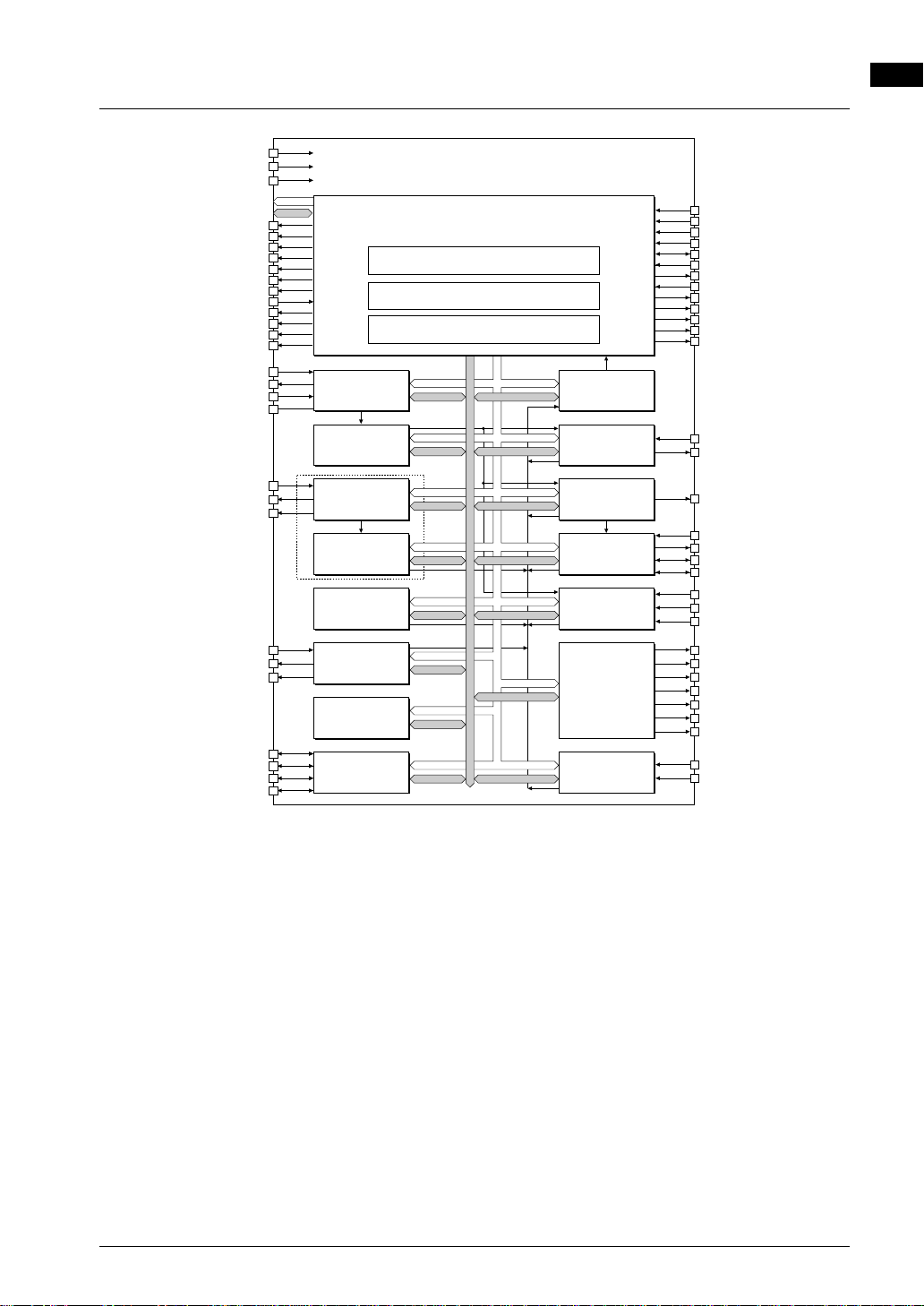
1.2 Block Diagram
V
DD
V
SS
V
DDE
A[23:0]
D[15:0]
#WRL/#WR/#WE
#HCAS, #LCAS, #RAS[1:0]
#CE10EX, #CE[9:3]
#DRD(P20), #DWE/#SDWE(P21)
#GAAS(P21), #GARD(P31)
SDA10, SDCKE, HDQM, LDQM
#DMAREQx(K50, K51, K53, K54)
#DMAACKx(P32, P33, P04, P06)
#DMAENDx(P15, P16, P05, P07)
#SDCAS, #SDRAS
#RD
#WRH/#BSH
#EMEMRD
#WAIT(P30)
#SDCE[1:0]
OSC3
OSC4
PLLS[1:0]
PLLC
OSC1
OSC2
FOSC1(P14)
P00–07
P10–16
P20–27
P30–35
OSC3/PLL
Prescaler
OSC1
Clock
Timer
Intelligent
DMA (128 ch.)
High-speed
DMA (4 ch.)
RAM
8KB
I/O Port
S1C33L03
S1C33000
CPU Core
Bus Control Unit
SDRAM Controller
Interrupt
Controller
16-bit
Programmable
Timer (6 ch.)
8-bit
Programmable
Timer (6 ch.)
Serial Interface
(4 ch.)
A/D Converter
(8 ch.)
LCD Controller
Input Port
1 OUTLINE
#RESET
#NMI
#X2SPD
ICEMD
DSIO
EA10MD[1:0]
BCLK
#BUSREQ(P34)
#BUSACK(P35)
#BUSGET(P31)
DST[2:0](P10–12)
DPCO(P13)
DCLK(P14)
EXCLx(P10–13, P15, P16)
TMx(P22–27)
T8UFx(P10–13)
SINx(P00, P04, P27, P33)
SOUTx(P01, P05, P26, P16)
#SCLKx(P02, P06, P25, P15)
#SRDYx(P03, P07, P24, P32)
AD0–7(K60–67)
#ADTRG(K52)
DDE
AV
FPDAT[7:4]
FPDAT[3:0]/GPO[6:3]
FPFRAME
FPLINE
FPSHIFT
DRDY(MOD/FPSHIFT2)
LCDPWR
K50–54
K60–67
A-1
Figure 1.2.1 S1C33L03 Block Diagram
S1C33L03 PRODUCT PART EPSON A-3
Page 20
1 OUTLINE
1.3 Pin Description
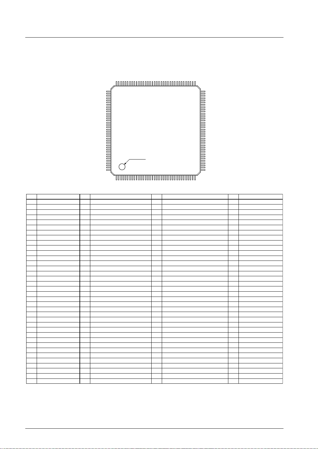
1.3.1 Pin Layout Diagram (plastic package)
QFP20-144pin
73108
No.
1
2
3
4
5
6
7
8
9
10
11
12
13
14
15
16
17
18
19
20
21
22
23
24
25
26
27
28
29
30
31
32
33
34
35
36
Pin name
P22/TM0
P23/TM1
SS
V
P24/TM2/#SRDY2
P25/TM3/#SCLK2
P26/TM4/SOUT2
P27/TM5/SIN2
DD
V
P07/#SRDY1/#DMAEND3
P06/#SCLK1/#DMAACK3
P05/SOUT1/#DMAEND2
P04/SIN1/#DMAACK2
FPDAT7
FPDAT6
FPDAT5
FPDAT4
FPDAT3/GPO6
FPDAT2/GPO5
FPDAT1/GPO4
FPDAT0/GPO3
DDE
V
DRDY(MOD/FPSHIFT2)
FPFRAME
FPLINE
FPSHIFT
LCDPWR
SS
V
K67/AD7
K66/AD6
K65/AD5
K64/AD4
K63/AD3
K62/AD2
K61/AD1
K60/AD0
DDE
AV
109
144
No.
37
K54/#DMAREQ3
38
K53/#DMAREQ2
39
K52/#ADTRG
40
K51/#DMAREQ1
41
K50/#DMAREQ0
42
#WRH/#BSH
43
#WRL/#WR/#WE
44
#RD
SS
45
V
D15
46
D14
47
D13
48
D12
49
D11
50
DD
V
51
D10
52
D9
53
D8
54
D7
55
D6
56
D5
57
D4
58
DDE
V
59
D3
60
D2
61
D1
62
D0
63
#CE8/#RAS1/#CE14/#RAS3/#SDCE1
64
#CE7/#RAS0/#CE13/#RAS2/#SDCE0
65
SS
V
66
OSC2
67
OSC1
68
#RESET
69
P35/#BUSACK/GPIO1
70
P34/#BUSREQ/#CE6/GPIO0
71
P33/#DMAACK1/SIN3/SDA10
72
Pin name
Figure 1.3.1 Pin Layout Diagram (QFP20-144pin)
INDEX
361
No.
73
P32/#DMAACK0/#SRDY3/HDQM
74
P31/#BUSGET/#GARD/GPIO2
75
P30/#WAIT/#CE4&5
76
#LCAS/#SDRAS
77
#HCAS/#SDCAS
DD
78
V
P21/#DWE/#GAAS/#SDWE
79
P20/#DRD/SDCKE
80
BCLK/SDCLK
81
SS
V
82
P16/EXCL5/#DMAEND1/SOUT3
83
P15/EXCL4/#DMAEND0/#SCLK3/LDQM
84
A0/#BSL
85
A1/SDA0
86
A2/SDA1
87
A3/SDA2
88
A4/SDA3
89
A5/SDA4
90
DDE
V
91
A6/SDA5
92
A7/SDA6
93
A8/SDA7
94
A9/SDA8
95
A10/SDA9
96
A11
97
SS
V
98
A12/SDA11
99
A13/SDA12
100
A14/SDBA0
101
A15/SDBA1
102
A16
103
A17
104
SS
V
105
A18
106
A19
107
A20
108
Pin name
72
37
No.
109
110
111
112
113
114
115
116
117
118
119
120
121
122
123
124
125
126
127
128
129
130
131
132
133
134
135
136
137
138
139
140
141
142
143
144
Pin name
A21
A22
A23
PLLS1
PLLS0
SS
V
PLLC
SS
V
DSIO
P14/FOSC1/DCLK
P13/EXCL3/T8UF3/DPCO
P12/EXCL2/T8UF2/DST2
P11/EXCL1/T8UF1/DST1
P10/EXCL0/T8UF0/DST0
EA10MD1
EA10MD0
ICEMD
#EMEMRD
DD
V
OSC4
OSC3
#NMI
#CE9/#CE17/#CE17&18
DDE
V
#CE5/#CE15/#CE15&16
N.C.
#CE3
SS
V
#CE10EX/#CE9&10EX
#CE6/#CE7&8
#CE4/#CE11/#CE11&12
#X2SPD
P03/#SRDY0
P02/#SCLK0
P01/SOUT0
P00/SIN0
A-4 EPSON S1C33L03 PRODUCT PART
Page 21
1.3.2 Pin Functions
Table 1.3.1 List of Pins for Power Supply System
Pin name Pin No. I/O Pull-up Function
VDD 8,51,78,127 – – Power supply (+) for the internal logic
VSS 3,27,45,66,
82,98,105,
114,116,136
VDDE 21,59,91,132 – – Power supply (+) for the I/O block
AVDDE 36 – – Analog system power supply (+); AVDDE = VDDE
Pin name Pin No. I/O Pull-up Function
A0
#BSL
A[10:1]
SDA[9:0]
A11 97 O – Address bus (A11)
A[13:12]
SDA[12:11]
A[15:14]
SDBA[1:0]
A[23:16] 103,104,
D[15:0] 46–50,52–58,
#CE10EX
#CE9&10EX
#CE9
#CE17
#CE17&18
#CE8
#RAS1
#CE14
#RAS3
#SDCE1
#CE7
#RAS0
#CE13
#RAS2
#SDCE0
#CE6
#CE7&8
#CE5
#CE15
#CE15&16
#CE4
#CE11
#CE11&12
#CE3 135 O – Area 3 chip enable
#RD 44 O – Read signal
#EMEMRD 126 O – Read signal for internal ROM emulation memory
85 O – A0: Address bus (A0) when SBUSST(D3/0x4812E) = "0" (default)
85–90,92–96 O
99,100 O – A[13:12]: A ddress bus (A12–A13)
101,102 O – A[15:14]: Address bus (A14–A15)
106–111
60–63
137 O – Area 10 chip enable for external memory
131 O – #CE9: Area 9 chip enable when CEFUNC[1:0](D[A:9]/0x48130) = "00" (default)
64 O – #CE8: Area 8 chip enable when CEFUNC[1:0](D[A:9]/0x48130) = "00",
65 O – #CE7: Area 7 chip enable when CEFUNC[1:0](D[A:9]/0x48130) = "00",
138 O – Area 6 chip enable
133 O – #CE5: Area 5 chip enable when CEFUNC[1:0](D[A:9]/0x48130) = "00" (default)
139 O – #CE4: Area 4 chip enable when CEFUNC[1:0](D[A:9]/0x48130) = "00" (default)
––Power supply (-); GND
Table 1.3.2 List of Pins for External Bus Interface Signals
#BSL: Bus strobe (low byte) signal when SBUSST(D3/0x4812E) = "1"
A[10:1]: Address bus (A1–A10)
–
SDA[9:0]: SDRAM address bus (SDA0–SDA9)
SDA[12:11]: SDRAM address bus (SDA11–SDA12)
O–Address bus (A16–A23)
I/O – Data bus (D0–D15)
SDBA[1:0]: SDRAM bank select (SDBA0–SDBA1)
* When CEFUNC[1:0] = "1x", this pin outputs #CE9+#CE10EX signal.
#CE17: Area 17 chip enable when CEFUNC[1:0](D[A:9]/0x48130) = "01"
* When CEFUNC[1:0] = "1x", this pin outputs #CE17+#CE18 signal.
A8DRA(D8/0x48128) = "0" and SDRPC1(D2/0x39FFC0) = "0" (default)
#RAS1: Area 8 DRAM row strobe when CEFUNC[1:0](D[A:9]/0x48130) = "00",
A8DRA(D8/0x48128) = "1" and SDRPC1(D2/0x39FFC0) = "0"
#CE14: Area 14 chip enable when CEFUNC[1:0](D[A:9]/0x48130) = "01" or "1x",
A14DRA(D8/0x48122) = "0" and SDRPC1(D2/0x39FFC0) = "0"
#RAS3: Area 14 DRAM row strobe when CEFUNC[1:0](D[A:9]/0x48130) = "01" or
"1x", A14DRA(D8/0x48122) = "1" and SDRPC1(D2/0x39FFC0) = "0"
#SDCE1: SDRAM chip enable 1 when SDRPC1(D2/0x39FFC0) = "1" and
SDRENA(D7/0x39FFC1) = "1"
A7DRA(D7/0x48128) = "0" and SDRPC0(D3/0x39FFC0) = "0" (default)
#RAS0: Area 7 DRAM row strobe when CEFUNC[1:0](D[A:9]/0x48130) = "00",
A7DRA(D7/0x48128) = "1" and SDRPC0(D3/0x39FFC0) = "0"
#CE13: Area 13 chip enable when CEFUNC[1:0](D[A:9]/0x48130) = "01" or "1x",
A13DRA(D7/0x48122) = "0" and SDRPC0(D3/0x39FFC0) = "0"
#RAS2: Area 13 DRAM row strobe when CEFUNC[1:0](D[A:9]/0x48130) = "01" or
"1x", A13DRA(D7/0x48122) = "1" and SDRPC0(D3/0x39FFC0) = "0"
#SDCE0: SDRAM chip enable 0 when SDRPC0(D3/0x39FFC0) = "1" and
SDRENA(D7/0x39FFC1) = "1"
* When CEFUNC[1:0] = "1x", this pin outputs #CE7+#CE8 signal.
#CE15: Area 15 chip enable when CEFUNC[1:0](D[A:9]/0x48130) = "01"
* When CEFUNC[1:0] = "1x", this pin outputs #CE15+#CE16 signal.
#CE11: Area 11 chip enable when CEFUNC[1:0](D[A:9]/0x48130) = "01"
* When CEFUNC[1:0] = "1x", this pin outputs #CE11+#CE12 signal.
1 OUTLINE
A-1
S1C33L03 PRODUCT PART EPSON A-5
Page 22
1 OUTLINE
Pin name Pin No. I/O Pull-up Function
#WRL
#WR
#WE
#WRH
#BSH
#HCAS
#SDCAS
#LCAS
#SDRAS
BCLK
SDCLK
P34
#BUSREQ
#CE6
GPIO0
P35
#BUSACK
GPIO1
P30
#WAIT
#CE4&5
P20
#DRD
SDCKE
P21
#DWE
#GAAS
#SDWE
P31
#BUSGET
#GARD
GPIO2
EA10MD1 123 I Pull-up Area 10 boot mode selection
EA10MD0 124 I – 1 1 External ROM mode
43 O – #WRL: Write (low byte) signal when SBUSST(D3/0x4812E) = "0" (default)
#WR: Write signal when SBUSST(D3/0x4812E) = "1"
#WE: DRAM write signal
42 O – #WRH: Write (high byte) signal when SBUSST(D3/0x4812E) = "0" (default)
#BSH: Bus strobe (high byte) signal when SBUSST(D3/0x4812E) = "1"
77 O – #HCAS: DRAM column address strobe (high byte) signal when
SDRENA(D7/0x39FFC1) = "0" (default)
#SDCAS: SDRAM column address strobe when SDRENA(D7/0x39FFC1) = "1"
76 O – #LCAS: DRAM column address strobe (low byte) signal when
SDRENA(D7/0x39FFC1) = "0" (default)
#SDRAS: SDRAM row address strobe when SDRENA(D7/0x39FFC1) = "1"
81 O – BCLK: Bus clock output when SDRENA(D7/0x39FFC1) = "0" (default)
SDCLK: SDRAM clock output when SDRENA(D7/0x39FFC1) = "1"
71 I/O – P34: I/O port when CFP34(D4/0x402DC) = "0" (default)
#BUSREQ: Bus release request input when CFP34(D4/0x402DC) = "1"
#CE6: Area 6 chip enable when CFP34(D4/0x402DC) = "1" and
IOC34(D4/0x402DE) = "1"
GPIO0: LCDC general-purpose I/O when LCDCEN(D5/0x39FFE3) = "1" and
BREQEN(D2/0x39FFFD) = "0"
70 I/O – P35: I/O port when CFP35(D5/0x402DC) = "0" (default)
#BUSACK: Bus acknowledge output when CFP35(D5/0x402DC) = "1" and
CFP34(D4/0x402DC) = "1"
GPIO1: LCDC general-purpose I/O when LCDCEN(D5/0x39FFE3) = "1" and
BREQEN(D2/0x39FFFD) = "0"
75 I/O – P30: I/O port when CFP30(D0/0x402DC) = "0" (default)
#WAIT: Wait cycle request input when CFP30(D0/0x402DC) = "1"
#CE4&5: Areas 4&5 chip enable when CFP30(D0/0x402DC) = "1" and
IOC30(D0/0x402DE) = "1"
80 I/O – P20: I/O port when CFP20(D0/0x402D8) = "0" and SDRENA(D7/0x39FFC1) =
"0" (default)
#DRD: DRAM read signal output for successive RAS mode when
CFP20(D0/0x402D8) = "1" and SDRENA(D7/0x39FFC1) = "0"
SDCKE: SDRAM clock enable signal when SDRENA(D7/0x39FFC1) = "1"
79 I/O – P21: I/O port when CFP21(D1/0x402D8) = "0", CFEX2(D2/0x402DF) = "0" and
SDRENA(D7/0x39FFC1) = "0" (default)
#DWE: DRAM write signal output for successive RAS mode when
CFP21(D1/0x402D8) = "1", CFEX2(D2/0x402DF) = "0" and
SDRENA(D7/0x39FFC1) = "0"
#GAAS: Area address strobe output for GA when CFEX2(D2/0x402DF) = "1" and
SDRENA(D7/0x39FFC1) = "0"
#SDWE: SDRAM write signal when SDRENA(D7/0x39FFC1) = "1"
74 I/O – P31: I/O port when CFP31(D1/0x402DC) = "0" and CFEX3(D3/0x402DF) = "0"
(default)
#BUSGET: Bus status monitor signal output for bus release request when
CFP31(D1/0x402DC) = "1" and CFEX3(D3/0x402DF) = "0"
#GARD: Area read signal output for GA when CFEX3(D3/0x402DF) = "1"
GPIO2: LCDC general-purpose I/O when LCDCEN(D5/0x39FFE3) = "1" and
BREQEN(D2/0x39FFFD) = "0"
EA10MD1 EA10MD0 Mode
10Internal ROM mode
A-6 EPSON S1C33L03 PRODUCT PART
Page 23
1 OUTLINE
Table 1.3.3 List of Pins for HSDMA Control Signals
Pin name Pin No. I/O P ull-up Function
K50
#DMAREQ0
K51
#DMAREQ1
K53
#DMAREQ2
K54
#DMAREQ3
P32
#DMAACK0
#SRDY3
HDQM
P33
#DMAACK1
SIN3
SDA10
P04
SIN1
#DMAACK2
P06
#SCLK1
#DMAACK3
P15
EXCL4
#DMAEND0
#SCLK3
LDQM
P16
EXCL5
#DMAEND1
SOUT3
P05
SOUT1
#DMAEND2
P07
#SRDY1
#DMAEND3
41 I Pull-up K50: Input port when CFK50(D0/0x402C0) = "0" (default)
#DMAREQ0: HSDMA Ch. 0 request input when CFK50(D0/0x402C0) = "1"
40 I Pull-up K51: Input port when CFK51(D1/0x402C0) = "0" (default)
#DMAREQ1: HSDMA Ch. 1 request input when CFK51(D1/0x402C0) = "1"
38 I Pull-up K53: Input port when CFK53(D3/0x402C0) = "0" (default)
#DMAREQ2: HSDMA Ch. 2 request input when CFK53(D3/0x402C0) = "1"
37 I Pull-up K54: Input port when CFK54(D4/0x402C0) = "0" (default)
#DMAREQ3: HSDMA Ch. 3 request input when CFK54(D4/0x402C0) = "1"
73 I/O – P32: I/O port when CFP32(D2/0x402DC) = "0" and SDRENA(D7/0x39FFC1) = "0"
(default)
#DMAACK0: HSDMA Ch. 0 acknowledge output when CFP32(D2/0x402DC) = "1" and
SDRENA(D7/0x39FFC1) = "0"
#SRDY3: Serial I/F Ch. 3 ready signal input/output when SSRDY3(D3/0x402D7) =
"1", CFP32(D2/0x402DC) = "0" and SDRENA(D7/0x39FFC1) = "0"
HDQM: SDRAM data (high byte) input/output mask signal when
SDRENA(D7/0x39FFC1) = "1"
72 I/O – P33: I/O port when CFP33(D3/0x402DC) = "0" and SDRENA(D7/0x39FFC1) = "0"
(default)
#DMAACK1: HSDMA Ch. 1 acknowledge output when CFP33(D3/0x402DC) = "1" and
SDRENA(D7/0x39FFC1) = "0"
SIN3:Serial I/F Ch. 3 data input when SSIN3(D0/0x402D7) = "1",
CFP33(D3/0x402DC) = "0" and SDRENA(D7/0x39FFC1) = "0"
SDA10: SDRAM address bus bit 10 when SDRENA(D7/0x39FFC1) = "1"
12 I/O – P04: I/O port when CFP04(D4/0x402D0) = "0" and CFEX4(D4/0x402DF) = "0"
(default)
SIN1:Serial I/F Ch. 1 data input when CFP04(D4/0x402D0) = "1" and
CFEX4(D4/0x402DF) = "0"
#DMAACK2: HSDMA Ch. 2 acknowledge output when CFEX4(D4/0x402DF) = "1"
10 I/O – P06: I/O port when CFP06(D6/0x402D0) = "0" and CFEX6(D6/0x402DF) = "0"
(default)
#SCLK1: Serial I/F Ch. 1 clock input/output when CFP06(D6/0x402D0) = "1" and
CFEX6(D6/0x402DF) = "0"
#DMAACK3: HSDMA Ch. 3 acknowledge output when CFEX6(D6/0x402DF) = "1"
84 I/O – P15: I/O port when CFP15(D5/0x402D4) = "0" and SDRENA(D7/0x39FFC1) = "0"
(default)
EXCL4: 16-bit timer 4 event counter input when CFP15(D5/0x402D4) = "1",
IOC15(D5/0x402D6) = "0" and SDRENA(D7/0x39FFC1) = "0"
#DMAEND0: HSDMA Ch. 0 end-of-transfer signal output when CFP15(D5/0x402D4) =
"1", IOC15(D5/0x402D6) = "1" and SDRENA(D7/0x39FFC1) = "0"
#SCLK3: Serial I/F Ch. 3 clock input/output when SSCLK3(D2/0x402D7) = "1",
CFP15(D5/0x402D4) = "0" and SDRENA(D7/0x39FFC1) = "0"
LDQM: SDRAM data (low byte) input/output mask signal when
SDRENA(D7/0x39FFC1) = "1"
83 I/O – P16: I/O port when CFP16(D6/0x402D4) = "0" (default)
EXCL5: 16-bit timer 5 event counter input when CFP16(D6/0x402D4) = "1" and
IOC16(D6/0x402D6) = "0"
#DMAEND1: HSDMA Ch. 1 end-of-transfer signal output when CFP16(D6/0x402D4) = "1"
and IOC16(D6/0x402D6) = "1"
SOUT3: Serial I/F Ch. 3 data output when SSOUT3(D1/0x402D7) = "1" and
CFP16(D6/0x402D4) = "0"
11 I/O – P05: I/O port when CFP05(D5/0x402D0) = "0" and CFEX5(D5/0x402DF) = "0"
(default)
SOUT1: Serial I/F Ch. 1 data output when CFP05(D5/0x402D0) = "1" and
CFEX5(D5/0x402DF) = "0"
#DMAEND2: HSDMA Ch. 2 end-of-transfer signal output when CFEX5(D5/0x402DF) = "1"
9 I/O – P07: I/O port when CFP07(D7/0x402D0) = "0" and CFEX7(D7/0x402DF) = "0"
(default)
#SRDY1: Serial I/F Ch. 1 ready signal output when CFP07(D7/0x402D0) = "1" and
CFEX5(D5/0x402DF) = "0"
#DMAEND3: HSDMA Ch. 3 end-of-transfer signal output when CFEX7(D7/0x402DF) = "1"
A-1
S1C33L03 PRODUCT PART EPSON A-7
Page 24
1 OUTLINE
Table 1.3.4 List of Pins for Internal Peripheral Circuits
Pin name Pin No. I/O Pull-up Function
K50
#DMAREQ0
K51
#DMAREQ1
K52
#ADTRG
K53
#DMAREQ2
K54
#DMAREQ3
K60
AD0
K61
AD1
K62
AD2
K63
AD3
K64
AD4
K65
AD5
K66
AD6
K67
AD7
P00
SIN0
P01
SOUT0
P02
#SCLK0
P03
#SRDY0
P04
SIN1
#DMAACK2
P05
SOUT1
#DMAEND2
P06
#SCLK1
#DMAACK3
P07
#SRDY1
#DMAEND3
P10
EXCL0
T8UF0
DST0
41 I Pull-up K50: Input port when CFK50(D0/0x402C0) = "0" (default)
#DMAREQ0: HSDMA Ch. 0 request input when CFK50(D0/0x402C0) = "1"
40 I Pull-up K51: Input port when CFK51(D1/0x402C0) = "0" (default)
#DMAREQ1: HSDMA Ch. 1 request input when CFK51(D1/0x402C0) = "1"
39 I Pull-up K52: Input port when CFK52(D2/0x402C0) = "0" (default)
#ADTRG: A/D converter trigger input when CFK52(D2/0x402C0) = "1"
38 I Pull-up K53: Input port when CFK53(D3/0x402C0) = "0" (default)
#DMAREQ2: HSDMA Ch. 2 request input when CFK53(D3/0x402C0) = "1"
37 I Pull-up K54: Input port when CFK54(D4/0x402C0) = "0" (default)
#DMAREQ3: HSDMA Ch. 3 request input when CFK54(D4/0x402C0) = "1"
35 I – K60: Input port when CFK60(D0/0x402C3) = "0" (default)
AD0: A/D converter Ch. 0 input when CFK60(D0/0x402C3) = "1"
34 I – K61: Input port when CFK61(D1/0x402C3) = "0" (default)
AD1: A/D converter Ch. 1 input when CFK61(D1/0x402C3) = "1"
33 I – K62: Input port when CFK62(D2/0x402C3) = "0" (default)
AD2: A/D converter Ch. 2 input when CFK62(D2/0x402C3) = "1"
32 I – K63: Input port when CFK63(D3/0x402C3) = "0" (default)
AD3: A/D converter Ch. 3 input when CFK63(D3/0x402C3) = "1"
31 I – K64: Input port when CFK64(D4/0x402C3) = "0" (default)
AD4: A/D converter Ch. 4 input when CFK64(D4/0x402C3) = "1"
30 I – K65: Input port when CFK65(D5/0x402C3) = "0" (default)
AD5: A/D converter Ch. 5 input when CFK65(D5/0x402C3) = "1"
29 I – K66: Input port when CFK66(D6/0x402C3) = "0" (default)
AD6: A/D converter Ch. 6 input when CFK66(D6/0x402C3) = "1"
28 I – K67: Input port when CFK67(D7/0x402C3) = "0" (default)
AD7: A/D converter Ch. 7 input when CFK67(D7/0x402C3) = "1"
144 I/O – P00: I/O port when CFP00(D0/0x402D0) = "0" (default)
SIN0:Serial I/F Ch. 0 data input when CFP00(D0/0x402D0) = "1"
143 I/O – P01: I/O port when CFP01(D1/0x402D0) = "0" (default)
SOUT0: Serial I/F Ch. 0 data output when CFP01(D1/0x402D0) = "1"
142 I/O – P02: I/O port when CFP02(D2/0x402D0) = "0" (default)
#SCLK0: Serial I/F Ch. 0 clock input/output when CFP02(D2/0x402D0) = "1"
141 I/O – P03: I/O port when CFP03(D3/0x402D0) = "0" (default)
#SRDY0: Serial I/F Ch. 0 ready signal input/output when CFP03(D3/0x402D0) = "1"
12 I/O – P04: I/O port when CFP04(D4/0x402D0) = "0" and CFEX4(D4/0x402DF) = "0"
(default)
SIN1:Serial I/F Ch. 1 data input when CFP04(D4/0x402D0) = "1" and
CFEX4(D4/0x402DF) = "0"
#DMAACK2: HSDMA Ch. 2 acknowledge output when CFEX4(D4/0x402DF) = "1"
11 I/O – P05: I/O port when CFP05(D5/0x402D0) = "0" and CFEX5(D5/0x402DF) = "0"
(default)
SOUT1: Serial I/F Ch. 1 data output when CFP05(D5/0x402D0) = "1" and
CFEX5(D5/0x402DF) = "0"
#DMAEND2: HSDMA Ch. 2 end-of-transfer signal output when
CFEX5(D5/0x402DF) = "1"
10 I/O – P06: I/O port when CFP06(D6/0x402D0) = "0" and CFEX6(D6/0x402DF) = "0"
(default)
#SCLK1: Serial I/F Ch. 1 clock input/output when CFP06(D6/0x402D0) = "1" and
CFEX6(D6/0x402DF) = "0"
#DMAACK3: HSDMA Ch. 3 acknowledge output when CFEX6(D6/0x402DF) = "1"
9 I/O – P07: I/O port when CFP07(D7/0x402D0) = "0" and CFEX7(D7/0x402DF) = "0"
(default)
#SRDY1: Serial I/F Ch. 1 ready signal output when CFP07(D7/0x402D0) = "1" and
CFEX5(D5/0x402DF) = "0"
#DMAEND3: HSDMA Ch. 3 end-of-transfer signal output when
CFEX7(D7/0x402DF) = "1"
122 I/O – P10: I/O port when CFP10(D0/0x402D4) = "0" and CFEX1(D1/0x402DF) = "0"
EXCL0: 16-bit timer 0 event counter input when CFP10(D0/0x402D4) = "1",
IOC10(D0/0x402D6) = "0" and CFEX1(D1/0x402DF) = "0"
T8UF0: 8-bit timer 0 output when CFP10(D0/0x402D4) = "1", IOC10(D0/0x402D6)
= "1" and CFEX1(D1/0x402DF) = "0"
DST0:DST0 signal output when CFEX1(D1/0x402DF) = "1" (default)
A-8 EPSON S1C33L03 PRODUCT PART
Page 25
1 OUTLINE
Pin name Pin No. I/O Pull-up Function
P11
EXCL1
T8UF1
DST1
P12
EXCL2
T8UF2
DST2
P13
EXCL3
T8UF3
DPCO
P14
FOSC1
DCLK
P15
EXCL4
#DMAEND0
#SCLK3
LDQM
P16
EXCL5
#DMAEND1
SOUT3
P20
#DRD
SDCKE
P21
#DWE
#GAAS
#SDWE
P22
TM0
P23
TM1
P24
TM2
#SRDY2
P25
TM3
#SCLK2
121 I/O – P11: I/O port when CFP11(D1/0x402D4) = "0" and CFEX1(D1/0x402DF) = "0"
EXCL1: 16-bit timer 1 event counter input when CFP11(D1/0x402D4) = "1",
IOC11(D1/0x402D6) = "0" and CFEX1(D1/0x402DF) = "0"
T8UF1: 8-bit timer 1 output when CFP11(D1/0x402D4) = "1", IOC11(D1/0x402D6)
= "1" and CFEX1(D1/0x402DF) = "0"
DST1:DST1 signal output when CFEX1(D1/0x402DF) = "1" (default)
120 I/O – P12: I/O port when CFP12(D2/0x402D4) = "0" and CFEX0(D0/0x402DF) = "0"
EXCL2: 16-bit timer 2 event counter input when CFP12(D2/0x402D4) = "1",
IOC12(D2/0x402D6) = "0" and CFEX0(D0/0x402DF) = "0"
T8UF2: 8-bit timer 2 output when CFP12(D2/0x402D4) = "1", IOC12(D2/0x402D6)
= "1" and CFEX0(D0/0x402DF) = "0"
DST2:DST2 signal output when CFEX0(D0/0x402DF) = "1" (default)
119 I/O – P13: I/O port when CFP13(D3/0x402D4) = "0" and CFEX1(D1/0x402DF) = "0"
EXCL3: 16-bit timer 3 event counter input when CFP13(D3/0x402D4) = "1",
IOC13(D3/0x402D6) = "0" and CFEX1(D1/0x402DF) = "0"
T8UF3: 8-bit timer 3 output when CFP13(D3/0x402D4) = "1", IOC13(D3/0x402D6)
= "1" and CFEX1(D1/0x402DF) = "0"
DPCO:DPCO signal output when CFEX1(D1/0x402DF) = "1" (default)
118 I/O – P14: I/O port when CFP14(D4/0x402D4) = "0" and CFEX0(D0/0x402DF) = "0"
FOSC1: OSC1 clock output when CFP14(D4/0x402D4) = "1" and
CFEX0(D0/0x402DF) = "0"
DCLK: DCLK signal output when CFEX0(D0/0x402DF) = "1" (default)
84 I/O – P15: I/O port when CFP15(D5/0x402D4) = "0" and SDRENA(D7/0x39FFC1)
= "0" (default)
EXCL4: 16-bit timer 4 event counter input when CFP15(D5/0x402D4) = "1",
IOC15(D5/0x402D6) = "0" and SDRENA(D7/0x39FFC1) = "0"
#DMAEND0: HSDMA Ch. 0 end-of-transfer signal output when CFP15(D5/0x402D4)
= "1", IOC15(D5/0x402D6) = "1" and SDRENA(D7/0x39FFC1) = "0"
#SCLK3: Serial I/F Ch. 3 clock input/output when SSCLK3(D2/0x402D7) = "1",
CFP15(D5/0x402D4) = "0" and SDRENA(D7/0x39FFC1) = "0"
LDQM: SDRAM data (low byte) input/output mask signal when
SDRENA(D7/0x39FFC1) = "1"
83 I/O – P16: I/O port when CFP16(D6/0x402D4) = "0" (default)
EXCL5: 16-bit timer 5 event counter input when CFP16(D6/0x402D4) = "1" and
IOC16(D6/0x402D6) = "0"
#DMAEND1: HSDMA Ch. 1 end-of-transfer signal output when CFP16(D6/0x402D4) =
"1" and IOC16(D6/0x402D6) = "1"
SOUT3: Serial I/F Ch. 3 data output when SSOUT3(D1/0x402D7) = "1" and
CFP16(D6/0x402D4) = "0"
80 I/O – P20: I/O port when CFP20(D0/0x402D8) = "0" and SDRENA(D7/0x39FFC1)
= "0" (default)
#DRD: DRAM read signal output for successive RAS mode when
CFP20(D0/0x402D8) = "1" and SDRENA(D7/0x39FFC1) = "0"
SDCKE: SDRAM clock enable signal when SDRENA(D7/0x39FFC1) = "1"
79 I/O – P21: I/O port when CFP21(D1/0x402D8) = "0", CFEX2(D2/0x402DF) = "0" and
SDRENA(D7/0x39FFC1) = "0" (default)
#DWE: DRAM write signal output for successive RAS mode when
CFP21(D1/0x402D8) = "1", CFEX2(D2/0x402DF) = "0" and
SDRENA(D7/0x39FFC1) = "0"
#GAAS: Area address strobe output for GA when CFEX2(D2/0x402DF) = "1" and
SDRENA(D7/0x39FFC1) = "0"
#SDWE: SDRAM write signal when SDRENA(D7/0x39FFC1) = "1"
1 I/O – P22: I/O port when CFP22(D2/0x402D8) = "0" (default)
TM0: 16-bit timer 0 output when CFP22(D2/0x402D8) = "1"
2 I/O – P23: I/O port when CFP23(D3/0x402D8) = "0" (default)
TM1: 16-bit timer 1 output when CFP23(D3/0x402D8) = "1"
4 I/O – P24: I/O port when CFP24(D4/0x402D8) = "0" (default)
TM2: 16-bit timer 2 output when CFP24(D4/0x402D8) = "1"
#SRDY2: Serial I/F Ch. 2 ready signal input/output when SSRDY2(D3/0x402DB) = "1"
and CFP24(D4/0x402D8) = "0"
5 I/O – P25: I/O port when CFP25(D5/0x402D8) = "0" (default)
TM3: 16-bit timer 3 output when CFP25(D5/0x402D8) = "1"
#SCLK2: Serial I/F Ch. 2 clock input/output when SSCLK2(D2/0x402DB) = "1" and
CFP25(D5/0x402D8) = "0"
A-1
S1C33L03 PRODUCT PART EPSON A-9
Page 26
1 OUTLINE
Pin name Pin No. I/O Pull-up Function
P26
TM4
SOUT2
P27
TM5
SIN2
P30
#WAIT
#CE4&5
P31
#BUSGET
#GARD
GPIO2
P32
#DMAACK0
#SRDY3
HDQM
P33
#DMAACK1
SIN3
SDA10
P34
#BUSREQ
#CE6
GPIO0
P35
#BUSACK
GPIO1
6 I/O – P26: I/O port when CFP26(D6/0x402D8) = "0" (default)
TM4: 16-bit timer 4 output when CFP26(D6/0x402D8) = "1"
SOUT2: Serial I/F Ch. 2 data output when SSOUT2(D1/0x402DB) = "1" and
CFP26(D6/0x402D8) = "0"
7 I/O – P27: I/O port when CFP27(D7/0x402D8) = "0" (default)
TM5: 16-bit timer 5 output when CFP27(D7/0x402D8) = "1"
SIN2:Serial I/F Ch. 2 data input when SSIN2(D0/0x402DB) = "1" and
CFP27(D7/0x402D8) = "0"
75 I/O – P30: I/O port when CFP30(D0/0x402DC) = "0" (default)
#WAIT: Wait cycle request input when CFP30(D0/0x402DC) = "1"
#CE4&5: Areas 4&5 chip enable when CFP30(D0/0x402DC) = "1" and
IOC30(D0/0x402DE) = "1"
74 I/O – P31: I/O port when CFP31(D1/0x402DC) = "0" and CFEX3(D3/0x402DF) = "0"
(default)
#BUSGET: Bus status monitor signal output for bus release request when
CFP31(D1/0x402DC) = "1" and CFEX3(D3/0x402DF) = "0"
#GARD: Area read signal output for GA when CFEX3(D3/0x402DF) = "1"
GPIO2: LCDC general-purpose I/O when LCDCEN(D5/0x39FFE3) = "1" and
BREQEN(D2/0x39FFFD) = "0"
73 I/O – P32: I/O port when CFP32(D2/0x402DC) = "0" and SDRENA(D7/0x39FFC1)
= "0" (default)
#DMAACK0: HSDMA Ch. 0 acknowledge output when CFP32(D2/0x402DC) = "1" and
SDRENA(D7/0x39FFC1) = "0"
#SRDY3: Serial I/F Ch. 3 ready signal input/output when SSRDY3(D3/0x402D7) =
"1", CFP32(D2/0x402DC) = "0" and SDRENA(D7/0x39FFC1) = "0"
HDQM: SDRAM data (high byte) input/output mask signal when
SDRENA(D7/0x39FFC1) = "1"
72 I/O – P33: I/O port when CFP33(D3/0x402DC) = "0" and SDRENA(D7/0x39FFC1)
= "0" (default)
#DMAACK1: HSDMA Ch. 1 acknowledge output when CFP33(D3/0x402DC) = "1" and
SDRENA(D7/0x39FFC1) = "0"
SIN3:Serial I/F Ch. 3 data input when SSIN3(D0/0x402D7) = "1",
CFP33(D3/0x402DC) = "0" and SDRENA(D7/0x39FFC1) = "0"
SDA10: SDRAM address bus bit 10 when SDRENA(D7/0x39FFC1) = "1"
71 I/O – P34: I/O port when CFP34(D4/0x402DC) = "0" (default)
#BUSREQ: Bus release request input when CFP34(D4/0x402DC) = "1"
#CE6: Area 6 chip enable when CFP34(D4/0x402DC) = "1" and
IOC34(D4/0x402DE) = "1"
GPIO0: LCDC general-purpose I/O when LCDCEN(D5/0x39FFE3) = "1" and
BREQEN(D2/0x39FFFD) = "0"
70 I/O – P35: I/O port when CFP35(D5/0x402DC) = "0" (default)
#BUSACK: Bus acknowledge output when CFP35(D5/0x402DC) = "1" and
CFP34(D4/0x402DC) = "1"
GPIO1: LCDC general-purpose I/O when LCDCEN(D5/0x39FFE3) = "1" and
BREQEN(D2/0x39FFFD) = "0"
A-10 EPSON S1C33L03 PRODUCT PART
Page 27
1 OUTLINE
Table 1.3.5 List of Pins for LCD Controller
Pin name Pin No. I/O Pull-up Function
FPDAT[7:4] 13–16 O – 4 high-order bits of data bus for 8-bit LCD panels
Data bus for 4-bit LCD panels
FPDAT[3:0]
GPO[6:3]
FPFRAME 23 O – Frame pulse output
FPLINE 24 O – Line pulse output
FPSHIFT 25 O – Shift clock output
DRDY(MOD)
(FPSHIFT2)
LCDPWR 26 O – LCD power control output (active high)
17–20 O – FPDAT[3:0]: 4 low-order bits of data bus for 8-bit LCD panels
GPO[6:3]: General-purpose outputs when a 4-bit LCD panel is used
22 O – MOD: LCD backplane bias (for panels other than 8-bit color panel format 1)
FPSHIFT2: Second shift clock (for 8-bit color panel format 1)
Table 1.3.6 List of Pins for Clock Generator
Pin name Pin No. I/O Pull-up Function
OSC1 68 I – Low-speed (OSC1) oscillation input (32 kHz crystal oscillator or external clock input)
OSC2 67 O – Low-speed (OSC1) oscillation output
OSC3 129 I – High-speed (OSC3) oscillation input (crystal/ceramic oscillator or external clock input)
OSC4 128 O – High-speed (OSC3) oscillation output
PLLS[1:0] 112,113 I – PLL set-up pins
PLLS1 PLLS0 fin (fOSC3)fout (fPSCIN)
1110–25MHz 20–50MHz
0110–12.5MHz 40–50MHz
00PLL is not used L
PLLC 115 – – Capacitor connecting pin for PLL
Table 1.3.7 List of Other Pins
Pin name Pin No. I/O
ICEMD 125 I Pull-
DSIO 117 I/O Pull-up Serial I/O pin for debugging
#X2SPD 140 I – Clock doubling mode set-up pin
#NMI 130 I Pull-up NMI request input pin
#RESET 69 I Pull-up Initial reset input pin
Pull-up
/down
High-impedance control input pin
down
When this pin is set to High, all the output pins go into high-impedance state. This makes
it possible to disable the S1C33 chip on the board.
This pin is used to communicate with the debugging tool S5U1C33000H.
1: CPU clock = bus clock × 1, 0: CPU clock = bus clock × 2
Function
A-1
Note: "#" in the pin names indicates that the signal is low active.
S1C33L03 PRODUCT PART EPSON A-11
Page 28
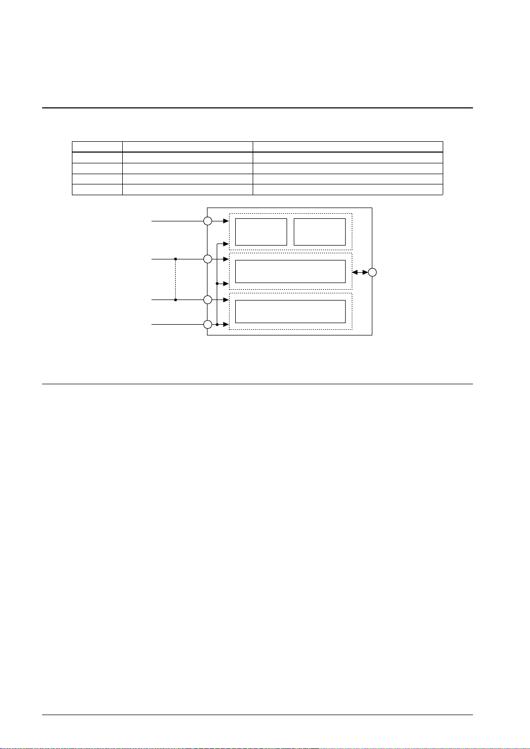
2 POWER SUPPLY
2 Power Supply
This chapter explains the operating voltage of the S1C33L03.
2.1 Power Supply Pins
The S1C3 3L03 has the power supply pins s hown in Tabl e 2.1.1.
Table 2.1.1 Power Supply Pins
Pin name Pin No. Function
VDD 8,51,78,127 Power supply (+) for the internal logic
VSS 3,27,45,66,82,98,105,114,116,136Power supply (-); GND
VDDE 21,59,91,132 Power supply (+) for the I/O block
AVDDE 36 A na log sys tem power supply (+); AV DDE = VDDE
V
AV
DD
CPU core
DDE
V
interface circuit
DDE
Analog circuits
(A/D converter)
V
SS
Internal
peripheral
circuit
I/O
1.8 to 3.6 V
1.8 to 5.5 V
1.8 to 5.5 V
GND
I/O pins
Figure 2.1.1 Power Supply System
2.2 Operating Voltage (VDD, VSS)
The core CPU and internal peripheral circuits operate with a voltage supplied between the VDD and VSS pins. The
following operating voltage can be used:
DD = 1.8 V to 3.6 V (VSS = GND)
V
Note: The S1 C33L03 has 4 V
pins. Do not open any of them.
The ope rating clock frequency range (OSC3) is 5 MHz to 50 MHz with this voltage.
DD pins an d 10 VSS pins. Be sure to supply the operating voltage to all the
A-12 EPSON S1C33L03 PRODUCT PART
Page 29

2 POWER SUPPLY
2.3 Power Supply for I/O Interface (VDDE)
The VDDE voltage is used for interfacing with external I/O signals. For the output interface of the S1C33L03, the
V
DDE voltage is used as high level and the VSS voltage as low level.
Normally, supply the same voltage level as V
pin is used for the ground common with VDD.
The following voltage is enabled for V
V
DDE = 1.8 V to 5.5 V (VSS = GND)
DD. It can be suppli ed separately from VDD for 5 V interface. The VSS
DDE:
A-1
A-2
Notes:•The S1C33L03 has 4 V
DDE pin s. Be sure t o supp l y a volta ge to al l the pins. Do not open any of
them.
•When an ext ernal clock is input to the OSC1 or OSC3 pin, the clock signal level must be V
•The interface voltage level of the DSIO, P10, P11, P12, P13 and P14 pins is V
DD.
DD.
2.4 Power Supply for Analog Circuits (AVDDE)
The analog power supply pin (AVDDE) is provided separately from the VDD and VDDE pins in order that the digital
circuits do not affect the analog circuit (A/D converter). The AV
and the V
Supply the same voltage level as the V
AV
Note: Be sure to supply V
SS pin is used as the analog ground.
DDE to the AVDDE pin.
DDE = VDDE, VSS = GND
DDE to the AVDDE pin even if the analog circu it is not used .
Noise on the analog power lines decrease the A/D converting precision, so use a stabilized power supply and make
the board pattern with consideration given to that.
DDE pin is used to supply an analog power voltage
S1C33L03 PRODUCT PART EPSON A-13
Page 30

3 INTERNAL MEMORY
3 In ternal Memory
This chapter explains the internal memory configuration.
Figure 3.1 shows the S1C33L 03 memory map.
Area
Areas 18–11
Area 10
Areas 9–7
Area 6
Areas 5–4
Area 3
Area 2
Area 1
Area 0
Address
0xFFFFFFF
0x1000000
0x0FFFFFF
0x0C00000
0x0BFFFFF
0x0400000
0x03FFFFF
0x0300000
0x02FFFFF
0x0100000
0x00FFFFF
0x0080000
0x007FFFF
0x0060000
0x005FFFF
0x0050000
0x004FFFF
0x0040000
0x003FFFF
0x0030000
0x002FFFF
0x0002000
0x0001FFF
0x0000000
Figure 3.1 Memory Map
For middleware use
For CPU, debug mode
Internal peripheral circuits
(Mirror of internal RAM)
Internal RAM (8KB)
External Memory
External Memory
External Memory
LCD controller
SDRAM controller
External Memory
(Reserved)
(Reserved)
(Mirror of internal
peripheral circuits)
(Mirror of internal
peripheral circuits)
Area 2 is use d in debug mo de only and it cannot be accessed in user mode (normal program execution status).
3.1 ROM and Boot Address
The S1C3 3L03 does no t have a built-in ROM. Th e boot add ress is fixed at 0x0C00000, a nd so externa l ROM/Fla sh
should be use d in Area 10.
For setting up Area 10, refer to the "BCU (Bus Control Unit)" in "S1C33L03 FUNCTION PART" in this manual.
A-14 EPSON S1C33L03 PRODUCT PART
Page 31

3 INTERNAL MEMORY
3.2 RAM
The S1C3 3L03 has a built -in 8KB RAM. The RAM is allocated to A rea 0, address 0x00 00000 to address
0x0001FFF.
The internal RAM is a 32-bit sized device and data can be read/written in 1 cycle regardless of data size (byte, halfword or word).
A-1
A-3
S1C33L03 PRODUCT PART EPSON A-15
Page 32

4 PERIPHERAL CIRCUITS
4 Peripheral Circuits
This chapter lists the built-in peripheral circuits and the I/O memory map. For details of the circuits, refer to the
"S1C33L03 FUNCTION PART".
4.1 List of Peripheral Circuits
The S1C33L03 consists of the C33 Co re Block, C33 SDRAM Contr oller Block, C33 Perip heral Block, C33 DMA
Block, C33 Analog Block, and C33 LCD Controll er Block.
C33 Core Block
CPU S1C33000 32-b it R I S C ty pe CPU
BCU (Bus Control Unit) 24-bit external address bus and 16-bit data bus
All the BCU functions can be used.
ITC (Interrupt Controller) 39 types of interrupts are available.
CLG (Clock Generator) OSC3 oscillation circuit (33 MHz Max.), PLL and OSC1 oscillation circuit
(32.768 kHz Typ.) built-in
DBG (Debug Unit) Functional block for debugging with the S5U1C 3 3000H (In-Cir cu i t D eb ug ger
for S1C33 Family)
C33 SDRAM Controller Block
SDRAM interface Up to two 128M-bit SDRAMs or a 256M-bit SDRAM (32MB) can be
connected directly.
C33 Peripheral Block
Prescaler Programmable clock generator for peripheral circuits
8-bit program mable timer 6 channels with clock output function
16-bit programmable timer 6 channels with event counter, clock output and watchdog timer functions
Serial interface 4 channels (asynchronous m ode, clock synchr on ous mode and IrDA are
selectable.)
Input and I/O ports 13 bits of input ports and 29 bits of I/O ports (used for peripheral I/O)
Clock timer 1 channel with alarm function
C33 DMA Block
HSDMA (High-Speed DMA) 4 channels
IDMA (Intelligent DMA) 128 channels
C33 Analog Block
A/D converter 10-bit A/D con verter with 8 input channels
C33 LCD Cont roller Block
LCD controller 4 or 8-bit monochrome/color LCD interface
2, 4 or 16-level (1, 2 or 4 bit- per-pixel) gray-scale display
2, 4, 16 or 256-level (1, 2, 4 or 8 bit- per-pixel) color display
Resolution examples : 640 × 480 pixel s with 1bpp color depth
640 × 240 pixels with 2bpp color depth
320 × 240 pixels with 4bpp color depth
240 × 160 pixels with 8bpp color depth
A-16 EPSON S1C33L03 PRODUCT PART
Page 33

4.2 I/O Memory Map
4 PERIPHERAL CIRCUITS
A-1
8-bit timer 4/5
clock select
register
8-bit timer 4/5
clock control
register
8-bit timer
clock select
register
16-bit timer 0
clock control
register
16-bit timer 1
clock control
register
16-bit timer 2
clock control
register
0040140
(B)
0040145
(B)
0040146
(B)
0040147
(B)
0040148
(B)
0040149
(B)
Table 4.2.1 I/O Memory Map
NameAddressRegister name Bit Function Setting Init. R/W Remarks
–
D7–2
D1
D0
D7
D6
D5
D4
D3
D2
D1
D0
D7–4
D3
D2
D1
D0
D7–4
D3
D2
D1
D0
D7–4
D3
D2
D1
D0
D7–4
D3
D2
D1
D0
P8TPCK5
P8TPCK4
P8TS52
P8TS51
P8TS50
P8TON4
P8TS42
P8TS41
P8TS40
P8TPCK3
P8TPCK2
P8TPCK1
P8TPCK0
P16TON0
P16TS02
P16TS01
P16TS00
P16TON1
P16TS12
P16TS11
P16TS10
P16TON2
P16TS22
P16TS21
P16TS20
reserved
8-bit timer 5 clock selection
8-bit timer 4 clock selection
8-bit timer 5 clock control
8-bit timer 5
clock division ratio selection
8-bit timer 4 clock control
8-bit timer 4
clock division ratio selection
reserved
8-bit timer 3 clock selection
8-bit timer 2 clock selection
8-bit timer 1 clock selection
8-bit timer 0 clock selection
reserved
16-bit timer 0 clock control
16-bit timer 0
clock division ratio selection
reserved
16-bit timer 1 clock control
16-bit timer 1
clock division ratio selection
reserved
16-bit timer 2 clock control
16-bit timer 2
clock division ratio selection
1 θ/1 0 Divided clk.
1 θ/1 0 Divided clk.
1 On 0 OffP8TON5
1
1
1
1
0
0
0
0
1 On 0 Off
1
1
1
1
0
0
0
0
1 θ/1 0 Divided clk.
1 θ/1 0 Divided clk.
1 θ/1 0 Divided clk.
1 θ/1 0 Divided clk.
1 On 0 Off
P16TS0[2:0] Division ratio
1
1
1
1
0
0
0
0
1 On 0 Off
P16TS1[2:0] Division ratio
1
1
1
1
0
0
0
0
1 On 0 Off
P16TS2[2:0] Division ratio
1
1
1
1
0
0
0
0
–
1
1
1
0
0
1
1
0
0
1
1
0
0
1
1
0
0
1
1
0
0
1
1
0
0
1
1
0
0
1
1
0
0
1
1
0
0
1
1
0
0
θ/256
0
θ/128
1
θ/64
0
θ/32
1
θ/16
0
θ/8
1
θ/4
0
θ/2
1
θ/4096
0
θ/2048
1
θ/64
0
θ/32
1
θ/16
0
θ/8
1
θ/4
0
θ/2
––
––
1
θ/4096
0
θ/1024
1
θ/256
0
θ/64
1
θ/16
0
θ/4
1
θ/2
0
θ/1
––
1
θ/4096
0
θ/1024
1
θ/256
0
θ/64
1
θ/16
0
θ/4
1
θ/2
0
θ/1
––
1
θ/4096
0
θ/1024
1
θ/256
0
θ/64
1
θ/16
0
θ/4
1
θ/2
0
θ/1
–
0
0
0
0
0
0
0
0
0
0
–
0
0
0
0
–
0
0
0
0
–
0
0
0
0
–
0
0
0
0
–
0 when being read.
R/W
θ: selected by
R/W
Prescaler clock select
register (0x40181)
R/W
θ: selected by
R/W
Prescaler clock select
R/W
register (0x40181)
R/W
8-bit timer 5 can
generate the clock for
the serial I/F Ch.3.
R/W
θ: selected by
R/W
Prescaler clock select
R/W
register (0x40181)
R/W
8-bit timer 4 can
generate the clock for
the serial I/F Ch.2.
–
0 when being read.
R/W
θ: selected by
R/W
Prescaler clock select
R/W
register (0x40181)
R/W
–
0 when being read.
R/W
θ: selected by
R/W
Prescaler clock select
register (0x40181)
16-bit timer 0 can be
used as a watchdog
timer.
–
0 when being read.
R/W
θ: selected by
R/W
Prescaler clock select
register (0x40181)
–
0 when being read.
R/W
θ: selected by
R/W
Prescaler clock select
register (0x40181)
A-4
(B) in [Address] indicates an 8-bit register and (HW) indicates a 16-bit register.
The meaning of the symbols described in [Init.] are listed below:
0, 1: Initial values that are set at initial reset.
(However, the registers for the bus and input/output ports are not initialized at hot start.)
X: Not initialized at initial reset.
–: N ot s et in the circuit.
S1C33L03 PRODUCT PART EPSON A-17
Page 34

4 PERIPHERAL CIRCUITS
16-bit timer 3
clock control
register
16-bit timer 4
clock control
register
16-bit timer 5
clock control
register
8-bit timer 0/1
clock control
register
004014A
004014B
004014C
004014D
(B)
(B)
(B)
(B)
D7–4
D3
D2
D1
D0
D7–4
D3
D2
D1
D0
D7–4
D3
D2
D1
D0
D7
D6
D5
D4
D3
D2
D1
D0
NameAddressRegister name Bit Function Setting Init. R/W Remarks
P16TON3
P16TS32
P16TS31
P16TS30
P16TON4
P16TS42
P16TS41
P16TS40
P16TON5
P16TS52
P16TS51
P16TS50
P8TS12
P8TS11
P8TS10
P8TON0
P8TS02
P8TS01
P8TS00
reserved
16-bit timer 3 clock control
16-bit timer 3
clock division ratio selection
reserved
16-bit timer 4 clock control
16-bit timer 4
clock division ratio selection
reserved
16-bit timer 5 clock control
16-bit timer 5
clock division ratio selection
8-bit timer 1 clock control
8-bit timer 1
clock division ratio selection
8-bit timer 0 clock control
8-bit timer 0
clock division ratio selection
1 On 0 Off
P16TS3[2:0] Division ratio
1
1
1
1
0
0
0
0
1 On 0 Off
P16TS4[2:0] Division ratio
1
1
1
1
0
0
0
0
1 On 0 Off
P16TS5[2:0] Division ratio
1
1
1
1
0
0
0
0
1 On 0 OffP8TON1
P8TS1[2:0] Division ratio
1
1
1
1
0
0
0
0
1 On 0 Off
P8TS0[2:0] Division ratio
1
1
1
1
0
0
0
0
––
1
1
1
0
0
1
1
0
0
1
1
0
0
1
1
0
0
1
1
0
0
1
1
0
0
1
1
0
0
1
1
0
0
1
1
0
0
1
1
0
0
θ/4096
0
θ/1024
1
θ/256
0
θ/64
1
θ/16
0
θ/4
1
θ/2
0
θ/1
––
1
θ/4096
0
θ/1024
1
θ/256
0
θ/64
1
θ/16
0
θ/4
1
θ/2
0
θ/1
––
1
θ/4096
0
θ/1024
1
θ/256
0
θ/64
1
θ/16
0
θ/4
1
θ/2
0
θ/1
1
θ/4096
0
θ/2048
1
θ/1024
0
θ/512
1
θ/256
0
θ/128
1
θ/64
0
θ/32
1
θ/256
0
θ/128
1
θ/64
0
θ/32
1
θ/16
0
θ/8
1
θ/4
0
θ/2
–
–
0
R/W
0
R/W
0
0
–
–
0
R/W
0
R/W
0
0
–
–
0
R/W
0
R/W
0
0
0
R/W
0
R/W
0
0
R/W
0
R/W
0
0
0
0 when being read.
θ: selected by
Prescaler clock select
register (0x40181)
0 when being read.
θ: selected by
Prescaler clock select
register (0x40181)
0 when being read.
θ: selected by
Prescaler clock select
register (0x40181)
θ: selected by
Prescaler clock select
register (0x40181)
8-bit timer 1 can
generate the OSC3
oscillation-stabilize
waiting period.
θ: selected by
Prescaler clock select
register (0x40181)
8-bit timer 0 can
generate the DRAM
refresh clock.
A-18 EPSON S1C33L03 PRODUCT PART
Page 35

4 PERIPHERAL CIRCUITS
8-bit timer 2/3
clock control
register
A/D clock
control register
Run/Stop
register
Clock timer
interrupt
control register
Clock timer
divider register
Clock timer
second
register
004014E
(B)
004014F
(B)
0040151
(B)
0040152
(B)
0040153
(B)
(B)
NameAddressRegister name Bit Function Setting Init. R/W Remarks
D7
D6
D5
D4
D3
D2
D1
D0
D7–4
D3
D2
D1
D0
D7–2
D1
D0
D7
D6
D5
D4
D3
D2
D1
D0
D7
D6
D5
D4
D3
D2
D1
D0
D7–6
D5
D4
D3
D2
D1
D0
P8TS32
P8TS31
P8TS30
P8TON2
P8TS22
P8TS21
P8TS20
–
PSONAD
PSAD2
PSAD1
PSAD0
–
TCRST
TCRUN
TCISE2
TCISE1
TCISE0
TCASE2
TCASE1
TCASE0
TCIF
TCAF
TCD7
TCD6
TCD5
TCD4
TCD3
TCD2
TCD1
TCD0
–
TCMD5
TCMD4
TCMD3
TCMD2
TCMD1
TCMD0
8-bit timer 3 clock control
8-bit timer 3
clock division ratio selection
8-bit timer 2 clock control
8-bit timer 2
clock division ratio selection
reserved
A/D converter clock control
A/D converter clock division ratio
selection
reserved
Clock timer reset
Clock timer Run/Stop control
Clock timer interrupt factor
selection
Clock timer alarm factor selection
Interrupt factor generation flag
Alarm factor generation flag
Clock timer data 1 Hz
Clock timer data 2 Hz
Clock timer data 4 Hz
Clock timer data 8 Hz
Clock timer data 16 Hz
Clock timer data 32 Hz
Clock timer data 64 Hz
Clock timer data 128 Hz
reserved
Clock timer second counter data
TCMD5 = MSB
TCMD0 = LSB
1 On 0 OffP8TON3
P8TS3[2:0] Division ratio
1
1
1
0
1
0
1
0
1
0
1
0
1
0
1
0
1
0
1
0
1
0
1
0
1
0
1
0
1
0
1
0
1
0
X
X
1
0
θ/256
θ/128
θ/64
θ/32
θ/16
θ/8
θ/4
θ/2
θ/4096
θ/2048
θ/64
θ/32
θ/16
θ/8
θ/4
θ/2
–
θ/256
θ/128
θ/64
θ/32
θ/16
θ/8
θ/4
θ/2
–Clock timer
None
Day
Hour
Minute
1 Hz
2 Hz
8 Hz
32 Hz
Day
Hour
Minute
None
Not generated
Not generated
–
1
1
1
0
1
0
0
1
0
1
0
0
0
0
1 On 0 Off
P8TS2[2:0] Division ratio
1
1
1
1
1
0
1
0
0
1
0
1
0
0
0
0
1 On 0 Off
P8TS0[2:0] Division ratio
1
1
1
1
1
0
1
0
0
1
0
1
0
0
0
0
1 Reset 0 Invalid
1 Run 0 Stop
TCISE[2:0] Interrupt factor
1
1
1
1
1
0
1
0
0
1
0
1
0
0
0
0
TCASE[2:0] Alarm factor
1
X
X
1
X
X
0
0
1 Generated 0
1 Generated 0
1 High 0 Low
1 High 0 Low
1 High 0 Low
1 High 0 Low
1 High 0 Low
1 High 0 Low
1 High 0 Low
1 High 0 Low
0 to 59 seconds
0
0
0
0
0
0
0
0
–
0
0
0
0
–
X
X
X
X
X
X
X
X
X
X
X
X
X
X
X
X
X
X
–
X
X
X
X
X
X
R/W
θ: selected by
R/W
Prescaler clock select
register (0x40181)
8-bit timer 3 can
generate the clock for
the serial I/F Ch.1.
R/W
θ: selected by
R/W
Prescaler clock select
register (0x40181)
8-bit timer 2 can
generate the clock for
the serial I/F Ch.0.
–
0 when being read.
R/W
θ: selected by
R/W
Prescaler clock select
register (0x40181)
–
0 when being read.
W
0 when being read.
R/W
R/W
R/W
Reset by writing 1.
R/W
Reset by writing 1.
R/W
R
R
R
R
R
R
R
R
–R0 when being read.0040154
A-1
A-4
S1C33L03 PRODUCT PART EPSON A-19
Page 36

4 PERIPHERAL CIRCUITS
Clock timer
minute register
Clock timer
hour register
Clock timer
day (low-order)
register
Clock timer
day (highorder) register
minute
comparison
register
hour
comparison
register
day
comparison
register
0040158
004015B
(B)
(B)
(B)
(B)
(B)
(B)
(B)
D7–6
D5
D4
D3
D2
D1
D0
D7–5
D4
D3
D2
D1
D0
D7
D6
D5
D4
D3
D2
D1
D0
D7
D6
D5
D4
D3
D2
D1
D0
D7–6
D5
D4
D3
D2
D1
D0
D7–5
D4
D3
D2
D1
D0
D7–5
D4
D3
D2
D1
D0
NameAddressRegister name Bit Function Setting Init. R/W Remarks
–
TCHD5
TCHD4
TCHD3
TCHD2
TCHD1
TCHD0
–
TCDD4
TCDD3
TCDD2
TCDD1
TCDD0
TCND7
TCND6
TCND5
TCND4
TCND3
TCND2
TCND1
TCND0
TCND14
TCND13
TCND12
TCND11
TCND10
TCND9
TCND8
–
TCCH5
TCCH4
TCCH3
TCCH2
TCCH1
TCCH0
–
TCCD4
TCCD3
TCCD2
TCCD1
TCCD0
–
TCCN4
TCCN3
TCCN2
TCCN1
TCCN0
reserved
Clock timer minute counter data
TCHD5 = MSB
TCHD0 = LSB
reserved
Clock timer hour counter data
TCDD4 = MSB
TCDD0 = LSB
Clock timer day counter data
(low-order 8 bits)
TCND0 = LSB
Clock timer day counter data
(high-order 8 bits)
TCND15 = MSB
reserved
Clock timer minute comparison
data
TCCH5 = MSB
TCCH0 = LSB
reserved
Clock timer hour comparison data
TCCD4 = MSB
TCCD0 = LSB
reserved
Clock timer day comparison data
TCCN4 = MSB
TCCN0 = LSB
–
0 to 59 minutes
–
0 to 23 hours
0 to 65535 days
(low-order 8 bits)
0 to 65535 days
(high-order 8 bits)
–Clock timer
0 to 59 minutes
(Note) Can be set within 0–63.
–Clock timer
0 to 23 hours
(Note) Can be set within 0–31.
–Clock timer
0 to 31 days
–
X
R/W
X
X
X
X
X
–
X
R/W
X
X
X
X
X
R/W0040157
X
X
X
X
X
X
X
X
R/WTCND15
X
X
X
X
X
X
X
–
X
R/W
X
X
X
X
X
–
X
R/W
X
X
X
X
–
X
R/W
X
X
X
X
–
0 when being read.0040155
–
0 when being read.0040156
–
0 when being read.0040159
–
0 when being read.004015A
–
0 when being read.
Compared with
TCND[4:0].
A-20 EPSON S1C33L03 PRODUCT PART
Page 37

4 PERIPHERAL CIRCUITS
8-bit timer 0
control register
8-bit timer 0
reload data
register
8-bit timer 0
counter data
register
8-bit timer 1
control register
8-bit timer 1
reload data
register
8-bit timer 1
counter data
register
8-bit timer 2
control register
8-bit timer 2
reload data
register
8-bit timer 2
counter data
register
0040160
(B)
(B)
(B)
0040164
(B)
(B)
(B)
0040168
(B)
(B)
(B)
NameAddressRegister name Bit Function Setting Init. R/W Remarks
–
D7–3
D2
D1
D0
D7
D6
D5
D4
D3
D2
D1
D0
D7
D6
D5
D4
D3
D2
D1
D0
D7–3
D2
D1
D0
D7
D6
D5
D4
D3
D2
D1
D0
D7
D6
D5
D4
D3
D2
D1
D0
D7–3
D2
D1
D0
D7
D6
D5
D4
D3
D2
D1
D0
D7
D6
D5
D4
D3
D2
D1
D0
PTOUT0
PSET0
PTRUN0
RLD06
RLD05
RLD04
RLD03
RLD02
RLD01
RLD00
PTD06
PTD05
PTD04
PTD03
PTD02
PTD01
PTD00
–
PTOUT1
PSET1
PTRUN1
RLD16
RLD15
RLD14
RLD13
RLD12
RLD11
RLD10
PTD16
PTD15
PTD14
PTD13
PTD12
PTD11
PTD10
–
PTOUT2
PSET2
PTRUN2
RLD26
RLD25
RLD24
RLD23
RLD22
RLD21
RLD20
PTD26
PTD25
PTD24
PTD23
PTD22
PTD21
PTD20
reserved
8-bit timer 0 clock output control
8-bit timer 0 preset
8-bit timer 0 Run/Stop control
8-bit timer 0 reload data
RLD07 = MSB
RLD00 = LSB
8-bit timer 0 counter data
PTD07 = MSB
PTD00 = LSB
reserved
8-bit timer 1 clock output control
8-bit timer 1 preset
8-bit timer 1 Run/Stop control
8-bit timer 1 reload data
RLD17 = MSB
RLD10 = LSB
8-bit timer 1 counter data
PTD17 = MSB
PTD10 = LSB
reserved
8-bit timer 2 clock output control
8-bit timer 2 preset
8-bit timer 2 Run/Stop control
8-bit timer 2 reload data
RLD27 = MSB
RLD20 = LSB
8-bit timer 2 counter data
PTD27 = MSB
PTD20 = LSB
1 On 0 Off
–
1 Preset 0 Invalid
1 Run 0 Stop
0 to 255RLD07
0 to 255PTD07
–
1 On 0 Off
1 Preset 0 Invalid
1 Run 0 Stop
0 to 255RLD17
0 to 255PTD17
–
1 On 0 Off
1 Preset 0 Invalid
1 Run 0 Stop
0 to 255RLD27
0 to 255PTD27
–
0
–
0
X
X
X
X
X
X
X
X
X
X
X
X
X
X
X
X
–
0
–
0
X
X
X
X
X
X
X
X
X
X
X
X
X
X
X
X
–
0
–
0
X
X
X
X
X
X
X
X
X
X
X
X
X
X
X
X
–
0 when being read.
R/W
0 when being read.
W
R/W
R/W0040161
R0040162
–
0 when being read.
R/W
0 when being read.
W
R/W
R/W0040165
R0040166
–
0 when being read.
R/W
0 when being read.
W
R/W
R/W0040169
R004016A
A-1
A-4
S1C33L03 PRODUCT PART EPSON A-21
Page 38

4 PERIPHERAL CIRCUITS
8-bit timer 3
control register
8-bit timer 3
reload data
register
8-bit timer 3
counter data
register
8-bit timer 4
control register
8-bit timer 4
reload data
register
8-bit timer 4
counter data
register
8-bit timer 5
control register
8-bit timer 5
reload data
register
8-bit timer 5
counter data
register
004016C
0040174
0040178
(B)
(B)
(B)
(B)
(B)
(B)
(B)
(B)
(B)
D7–3
D2
D1
D0
D7
D6
D5
D4
D3
D2
D1
D0
D7
D6
D5
D4
D3
D2
D1
D0
D7–3
D2
D1
D0
D7
D6
D5
D4
D3
D2
D1
D0
D7
D6
D5
D4
D3
D2
D1
D0
D7–3
D2
D1
D0
D7
D6
D5
D4
D3
D2
D1
D0
D7
D6
D5
D4
D3
D2
D1
D0
NameAddressRegister name Bit Function Setting Init. R/W Remarks
–
PTOUT3
PSET3
PTRUN3
RLD36
RLD35
RLD34
RLD33
RLD32
RLD31
RLD30
PTD36
PTD35
PTD34
PTD33
PTD32
PTD31
PTD30
–
PTOUT4
PSET4
PTRUN4
RLD46
RLD45
RLD44
RLD43
RLD42
RLD41
RLD40
PTD46
PTD45
PTD44
PTD43
PTD42
PTD41
PTD40
–
PTOUT5
PSET5
PTRUN5
RLD56
RLD55
RLD54
RLD53
RLD52
RLD51
RLD50
PTD56
PTD55
PTD54
PTD53
PTD52
PTD51
PTD50
reserved
8-bit timer 3 clock output control
8-bit timer 3 preset
8-bit timer 3 Run/Stop control
8-bit timer 3 reload data
RLD37 = MSB
RLD30 = LSB
8-bit timer 3 counter data
PTD37 = MSB
PTD30 = LSB
reserved
8-bit timer 4 clock output control
8-bit timer 4 preset
8-bit timer 4 Run/Stop control
8-bit timer 4 reload data
RLD47 = MSB
RLD40 = LSB
8-bit timer 4 counter data
PTD47 = MSB
PTD40 = LSB
reserved
8-bit timer 5 clock output control
8-bit timer 5 preset
8-bit timer 5 Run/Stop control
8-bit timer 5 reload data
RLD57 = MSB
RLD50 = LSB
8-bit timer 5 counter data
PTD57 = MSB
PTD50 = LSB
1 On 0 Off
–
1 Preset 0 Invalid
1 Run 0 Stop
0 to 255RLD37
0 to 255PTD37
–
1 On 0 Off
1 Preset 0 Invalid
1 Run 0 Stop
0 to 255RLD47
0 to 255PTD47
–
1 On 0 Off
1 Preset 0 Invalid
1 Run 0 Stop
0 to 255RLD57
0 to 255PTD57
–
0
R/W
–
0
R/W
X
R/W004016D
X
X
X
X
X
X
X
X
X
X
X
X
X
X
X
–
0
R/W
–
0
R/W
X
R/W0040175
X
X
X
X
X
X
X
X
X
X
X
X
X
X
X
–
0
R/W
–
0
R/W
X
R/W0040179
X
X
X
X
X
X
X
X
X
X
X
X
X
X
X
–
0 when being read.
0 when being read.
W
R004016E
–
0 when being read.
0 when being read.
W
R0040176
–
0 when being read.
0 when being read.
W
R004017A
A-22 EPSON S1C33L03 PRODUCT PART
Page 39

4 PERIPHERAL CIRCUITS
Watchdog
timer writeprotect register
Watchdog
timer enable
register
0040170
(B)
0040171
(B)
NameAddressRegister name Bit Function Setting Init. R/W Remarks
WRWD
D7
D6–0
D7–2
D1
D0
–
–
EWD
–
EWD write protection
–
–
Watchdog timer enable
–
1
Write enabled0Write-protect
1
NMI enabled0NMI disabled
–
–
–
0–R/W
–
0
–
0 when being read.
–
–
0 when being read.
R/W
0 when being read.
–
A-1
A-4
S1C33L03 PRODUCT PART EPSON A-23
Page 40

4 PERIPHERAL CIRCUITS
Power control
register
select register
Clock option
register
Power control
protect register
0040180
0040181
0040190
(B)
(B)
(B)
(B)
D7
D6
D5
D4–3
D2
D1
D0
D7–1
D0
D7–4
D3
D2
D1
D0
D7
D6
D5
D4
D3
D2
D1
D0
NameAddressRegister name Bit Function Setting Init. R/W Remarks
CLKDT1
CLKDT0
PSCON
–
CLKCHG
SOSC3
SOSC1
–
PSCDT0
–
HLT2OP
8T1ON
–
PF1ON
CLGP7
CLGP6
CLGP5
CLGP4
CLGP3
CLGP2
CLGP1
CLGP0
System clock division ratio
selection
Prescaler On/Off control
reserved
CPU operating clock switch
High-speed (OSC3) oscillation On/Off
Low-speed (OSC1) oscillation On/Off
reserved
Prescaler clock selection
–
HALT clock option
OSC3-stabilize waiting function
reserved
OSC1 external output control
Power control register protect flag 0
CLKDT[1:0] Division ratio
1
1
1
0
0
1
0
0
1 On 0 Off
1 OSC3 0 OSC1
1 On 0 Off
1 On 0 Off
1/8
1/4
1/2
1/1
–
–Prescaler clock
1 OSC1 0 OSC3/PLL
1 On 0 Off
1 Off 0 On
1 On 0 Off
Writing 10010110 (0x96)
removes the write protection of
the power control register
(0x40180) and the clock option
register (0x40190).
Writing another value set the
write protection.
–
–
0
0
1
0
1
1
1
00–
–
0
1
0
0
0
0
0
0
0
0
0
R/W
R/W
–
R/W
R/W
R/W
R/W
–
R/W
R/W
–
R/W
R/W004019E
Writing 1 not allowed.
0 when being read.
Do not write 1.
A-24 EPSON S1C33L03 PRODUCT PART
Page 41

4 PERIPHERAL CIRCUITS
Serial I/F Ch.0
transmit data
register
Serial I/F Ch.0
receive data
register
Serial I/F Ch.0
status register
Serial I/F Ch.0
control register
Serial I/F Ch.0
IrDA register
00401E0
(B)
00401E1
(B)
00401E2
(B)
00401E3
(B)
00401E4
(B)
NameAddressRegister name Bit Function Setting Init. R/W Remarks
D7
D6
D5
D4
D3
D2
D1
D0
D7
D6
D5
D4
D3
D2
D1
D0
D7–6
D5
D4
D3
D2
D1
D0
D7
D6
D5
D4
D3
D2
D1
D0
D7–5
D4
D3
D2
D1
D0
TXD06
TXD05
TXD04
TXD03
TXD02
TXD01
TXD00
RXD06
RXD05
RXD04
RXD03
RXD02
RXD01
RXD00
–
TEND0
FER0
PER0
OER0
TDBE0
RDBF0
TXEN0
RXEN0
EPR0
PMD0
STPB0
SSCK0
SMD01
SMD00
–
DIVMD0
IRTL0
IRRL0
IRMD01
IRMD00
Serial I/F Ch.0 transmit data
TXD07(06) = MSB
TXD00 = LSB
Serial I/F Ch.0 receive data
RXD07(06) = MSB
RXD00 = LSB
–
Ch.0 transmit-completion flag
Ch.0 flaming error flag
Ch.0 parity error flag
Ch.0 overrun error flag
Ch.0 transmit data buffer empty
Ch.0 receive data buffer full
Ch.0 transmit enable
Ch.0 receive enable
Ch.0 parity enable
Ch.0 parity mode selection
Ch.0 stop bit selection
Ch.0 input clock selection
Ch.0 transfer mode selection
–
Ch.0 async. clock division ratio
Ch.0 IrDA I/F output logic inversion
Ch.0 IrDA I/F input logic inversion
Ch.0 interface mode selection
0x0 to 0xFF(0x7F)TXD07
0x0 to 0xFF(0x7F)RXD07
1
Transmitting
1 Error 0 Normal
1 Error 0 Normal
1 Error 0 Normal
1 Empty 0 Buffer full
1 Buffer full 0 Empty
1 Enabled 0 Disabled
1 Enabled 0 Disabled
1 With parity 0 No parity
1 Odd 0 Even
1 2 bits 0 1 bit
1 #SCLK0 0
SMD0[1:0] Transfer mode
1
1
0
0
1 1/8 0 1/16
1 Inverted 0 Direct
1 Inverted 0 Direct
IRMD0[1:0]–I/F mode
1
1
0
0
–
0 End
Internal clock
1
8-bit asynchronous
0
7-bit asynchronous
Clock sync. Slave
1
Clock sync. Master
0
1
reserved
0
IrDA 1.0
1
reserved
0
General I/F
X
X
X
X
X
X
X
X
X
X
X
X
X
X
X
X
–
0
0
0
0
1
0
0
0
X
X
X
X
X
X
–
X
X
X
X
X
R/W 7-bit asynchronous
mode does not use
TXD07.
R 7-bit asynchronous
mode does not use
RXD07 (fixed at 0).
–
0 when being read.
R
Reset by writing 0.
R/W
Reset by writing 0.
R/W
Reset by writing 0.
R/W
R
R
R/W
R/W
Valid only in
R/W
asynchronous mode.
R/W
R/W
R/W
R/W
–
0 when being read.
R/W
Valid only in
R/W
asynchronous mode.
R/W
R/W
A-1
A-4
S1C33L03 PRODUCT PART EPSON A-25
Page 42

4 PERIPHERAL CIRCUITS
Serial I/F Ch.1
transmit data
register
Serial I/F Ch.1
receive data
register
Serial I/F Ch.1
status register
Serial I/F Ch.1
control register
Serial I/F Ch.1
IrDA register
Serial I/F Ch.2
transmit data
register
Serial I/F Ch.2
receive data
register
Serial I/F Ch.2
status register
00401E5
00401E6
00401E7
00401E8
00401E9
00401F2
(B)
(B)
(B)
(B)
(B)
(B)
(B)
(B)
D7
D6
D5
D4
D3
D2
D1
D0
D7
D6
D5
D4
D3
D2
D1
D0
D7–6
D5
D4
D3
D2
D1
D0
D7
D6
D5
D4
D3
D2
D1
D0
D7–5
D4
D3
D2
D1
D0
D7
D6
D5
D4
D3
D2
D1
D0
D7
D6
D5
D4
D3
D2
D1
D0
D7–6
D5
D4
D3
D2
D1
D0
NameAddressRegister name Bit Function Setting Init. R/W Remarks
TXD16
TXD15
TXD14
TXD13
TXD12
TXD11
TXD10
RXD16
RXD15
RXD14
RXD13
RXD12
RXD11
RXD10
–
TEND1
FER1
PER1
OER1
TDBE1
RDBF1
TXEN1
RXEN1
EPR1
PMD1
STPB1
SSCK1
SMD11
SMD10
–
DIVMD1
IRTL1
IRRL1
IRMD11
IRMD10
TXD26
TXD25
TXD24
TXD23
TXD22
TXD21
TXD20
RXD26
RXD25
RXD24
RXD23
RXD22
RXD21
RXD20
–
TEND2
FER2
PER2
OER2
TDBE2
RDBF2
Serial I/F Ch.1 transmit data
TXD17(16) = MSB
TXD10 = LSB
Serial I/F Ch.1 receive data
RXD17(16) = MSB
RXD10 = LSB
–
Ch.1 transmit-completion flag
Ch.1 flaming error flag
Ch.1 parity error flag
Ch.1 overrun error flag
Ch.1 transmit data buffer empty
Ch.1 receive data buffer full
Ch.1 transmit enable
Ch.1 receive enable
Ch.1 parity enable
Ch.1 parity mode selection
Ch.1 stop bit selection
Ch.1 input clock selection
Ch.1 transfer mode selection
–
Ch.1 async. clock division ratio
Ch.1 IrDA I/F output logic inversion
Ch.1 IrDA I/F input logic inversion
Ch.1 interface mode selection
Serial I/F Ch.2 transmit data
TXD27(26) = MSB
TXD20 = LSB
Serial I/F Ch.2 receive data
RXD27(26) = MSB
RXD20 = LSB
reserved
Ch.2 transmit-completion flag
Ch.2 flaming error flag
Ch.2 parity error flag
Ch.2 overrun error flag
Ch.2 transmit data buffer empty
Ch.2 receive data buffer full
0x0 to 0xFF(0x7F)TXD17
0x0 to 0xFF(0x7F)RXD17
1
Transmitting
1 Error 0 Normal
1 Error 0 Normal
1 Error 0 Normal
1 Empty 0 Buffer full
1 Buffer full 0 Empty
1 Enabled 0 Disabled
1 Enabled 0 Disabled
1 With parity 0 No parity
1 Odd 0 Even
1 2 bits 0 1 bit
1 #SCLK1 0
SMD1[1:0] Transfer mode
1
1
0
0
1 1/8 0 1/16
1 Inverted 0 Direct
1 Inverted 0 Direct
IRMD1[1:0]–I/F mode
1
1
0
0
1
Transmitting
1 Error 0 Normal
1 Error 0 Normal
1 Error 0 Normal
1 Empty 0 Buffer full
1 Buffer full 0 Empty
–
1
8-bit asynchronous
0
7-bit asynchronous
Clock sync. Slave
1
Clock sync. Master
0
1
0
1
0
0x0 to 0xFF(0x7F)TXD27
0x0 to 0xFF(0x7F)RXD27
–
0 End
Internal clock
reserved
IrDA 1.0
reserved
General I/F
0 End
X
R/W 7-bit asynchronous
X
mode does not use
X
TXD17.
X
X
X
X
X
X
R 7-bit asynchronous
X
mode does not use
X
RXD17 (fixed at 0).
X
X
X
X
X
–
–
0 when being read.
0
R
Reset by writing 0.
0
R/W
Reset by writing 0.
0
R/W
Reset by writing 0.
0
R/W
1
R
0
R
0
R/W
0
R/W
Valid only in
X
R/W
asynchronous mode.
X
R/W
X
R/W
X
R/W
X
R/W
X
–
–
0 when being read.
X
R/W
Valid only in
X
R/W
asynchronous mode.
X
R/W
X
R/W
X
X
R/W00401F0
X
X
X
X
X
X
X
X
R00401F1
X
X
X
X
X
X
X
–
–
0 when being read.
0
R
Reset by writing 0.
0
R/W
Reset by writing 0.
0
R/W
Reset by writing 0.
0
R/W
1
R
0
R
A-26 EPSON S1C33L03 PRODUCT PART
Page 43

4 PERIPHERAL CIRCUITS
Serial I/F Ch.2
control register
Serial I/F Ch.2
IrDA register
Serial I/F Ch.3
transmit data
register
Serial I/F Ch.3
receive data
register
Serial I/F Ch.3
status register
Serial I/F Ch.3
control register
Serial I/F Ch.3
IrDA register
00401F3
(B)
00401F4
(B)
(B)
(B)
00401F7
(B)
00401F8
(B)
00401F9
(B)
NameAddressRegister name Bit Function Setting Init. R/W Remarks
TXEN2
D7
D6
D5
D4
D3
D2
D1
D0
D7–5
D4
D3
D2
D1
D0
D7
D6
D5
D4
D3
D2
D1
D0
D7
D6
D5
D4
D3
D2
D1
D0
D7–6
D5
D4
D3
D2
D1
D0
D7
D6
D5
D4
D3
D2
D1
D0
D7–5
D4
D3
D2
D1
D0
RXEN2
EPR2
PMD2
STPB2
SSCK2
SMD21
SMD20
–
DIVMD2
IRTL2
IRRL2
IRMD21
IRMD20
TXD36
TXD35
TXD34
TXD33
TXD32
TXD31
TXD30
RXD36
RXD35
RXD34
RXD33
RXD32
RXD31
RXD30
–
TEND3
FER3
PER3
OER3
TDBE3
RDBF3
TXEN3
RXEN3
EPR3
PMD3
STPB3
SSCK3
SMD31
SMD30
–
DIVMD3
IRTL3
IRRL3
IRMD31
IRMD30
Ch.2 transmit enable
Ch.2 receive enable
Ch.2 parity enable
Ch.2 parity mode selection
Ch.2 stop bit selection
Ch.2 input clock selection
Ch.2 transfer mode selection
reserved
Ch.2 async. clock division ratio
Ch.2 IrDA I/F output logic inversion
Ch.2 IrDA I/F input logic inversion
Ch.2 interface mode selection
Serial I/F Ch.3 transmit data
TXD37(36) = MSB
TXD30 = LSB
Serial I/F Ch.3 receive data
RXD37(36) = MSB
RXD30 = LSB
reserved
Ch.3 transmit-completion flag
Ch.3 flaming error flag
Ch.3 parity error flag
Ch.3 overrun error flag
Ch.3 transmit data buffer empty
Ch.3 receive data buffer full
Ch.3 transmit enable
Ch.3 receive enable
Ch.3 parity enable
Ch.3 parity mode selection
Ch.3 stop bit selection
Ch.3 input clock selection
Ch.3 transfer mode selection
reserved
Ch.3 async. clock division ratio
Ch.3 IrDA I/F output logic inversion
Ch.3 IrDA I/F input logic inversion
Ch.3 interface mode selection
1 Enabled 0 Disabled
1 Enabled 0 Disabled
1 With parity 0 No parity
1 Odd 0 Even
1 2 bits 0 1 bit
1 #SCLK2 0
SMD2[1:0] Transfer mode
1
1
0
0
1 1/8 0 1/16
1 Inverted 0 Direct
1 Inverted 0 Direct
IRMD2[1:0]–I/F mode
1
1
0
0
0x0 to 0xFF(0x7F)TXD37
0x0 to 0xFF(0x7F)RXD37
1
Transmitting
1 Error 0 Normal
1 Error 0 Normal
1 Error 0 Normal
1 Empty 0 Buffer full
1 Buffer full 0 Empty
1 Enabled 0 Disabled
1 Enabled 0 Disabled
1 With parity 0 No parity
1 Odd 0 Even
1 2 bits 0 1 bit
1 #SCLK3 0
SMD3[1:0] Transfer mode
1
1
0
0
1 1/8 0 1/16
1 Inverted 0 Direct
1 Inverted 0 Direct
IRMD3[1:0]–I/F mode
1
1
0
0
Internal clock
1
8-bit asynchronous
0
7-bit asynchronous
Clock sync. Slave
1
Clock sync. Master
0
1
reserved
0
IrDA 1.0
1
reserved
0
General I/F
–
0 End
Internal clock
1
8-bit asynchronous
0
7-bit asynchronous
Clock sync. Slave
1
Clock sync. Master
0
1
reserved
0
IrDA 1.0
1
reserved
0
General I/F
0
0
X
X
X
X
X
X
–
X
X
X
X
X
X
X
X
X
X
X
X
X
X
X
X
X
X
X
X
X
–
0
0
0
0
1
0
0
0
X
X
X
X
X
X
–
X
X
X
X
X
R/W
R/W
Valid only in
R/W
asynchronous mode.
R/W
R/W
R/W
R/W
–
0 when being read.
R/W
Valid only in
R/W
asynchronous mode.
R/W
R/W
R/W00401F5
R00401F6
–
0 when being read.
R
Reset by writing 0.
R/W
Reset by writing 0.
R/W
Reset by writing 0.
R/W
R
R
R/W
R/W
Valid only in
R/W
asynchronous mode.
R/W
R/W
R/W
R/W
–
0 when being read.
R/W
Valid only in
R/W
asynchronous mode.
R/W
R/W
A-1
A-4
S1C33L03 PRODUCT PART EPSON A-27
Page 44

4 PERIPHERAL CIRCUITS
A/D conversion
result (loworder) register
A/D conversion
result (highorder) register
A/D trigger
register
A/D channel
register
A/D enable
register
A/D sampling
register
0040244
0040245
(B)
(B)
(B)
(B)
(B)
(B)
D7
D6
D5
D4
D3
D2
D1
D0
D7–2
D1
D0
D7–6
D5
D4
D3
D2
D1
D0
D7–6
D5
D4
D3
D2
D1
D0
D7–4
D3
D2
D1
D0
D7–2
D1
D0
NameAddressRegister name Bit Function Setting Init. R/W Remarks
ADD7
ADD6
ADD5
ADD4
ADD3
ADD2
ADD1
ADD0
ADD9
ADD8
–
MS
TS1
TS0
CH2
CH1
CH0
–
CE2
CE1
CE0
CS2
CS1
CS0
–
ADF
ADE
ADST
OWE
–
ST1
ST0
A/D converted data
(low-order 8 bits)
ADD0 = LSB
–
A/D converted data
(high-order 2 bits) ADD9 = MSB
–
A/D conversion mode selection
A/D conversion trigger selection
A/D conversion channel status
–
A/D converter
end channel selection
A/D converter
start channel selection
–
Conversion-complete flag
A/D enable
A/D conversion control/status
Overwrite error flag
–
Input signal sampling time setup
0x0 to 0x3FF
(low-order 8 bits)
––
0x0 to 0x3FF
(high-order 2 bits)
1
1
0
0
1
1
0
0
1
1
0
0
1
1
0
0
1
1
0
0
1
1
0
0
1
0
1
0
1
0
1
0
1
0
1
0
1
0
1
0
1
0
1
0
1
0
1
0
1
0
1
0
–
Trigger
#ADTRG pin
8-bit timer 0
16-bit timer 0
Software
AD7
AD6
AD5
AD4
AD3
AD2
AD1
AD0
–
AD7
AD6
AD5
AD4
AD3
AD2
AD1
AD0
AD7
AD6
AD5
AD4
AD3
AD2
AD1
AD0
1 Continuous 0 Normal
TS[1:0]
1
1
0
0
CH[2:0] Channel
1
1
1
1
0
0
0
0
CE[2:0] End channel
1
1
1
1
0
0
0
0
CS[2:0] Start channel
1
1
1
1
0
0
0
0
– –
1 Completed 0
Run/Standby
1 Enabled 0 Disabled
1 Start/Run 0 Stop
1 Error 0 Normal
ST[1:0] Sampring time
1
1
0
0
–
1
9 clocks
0
7 clocks
1
5 clocks
0
3 clocks
0
R0040240
0
0
0
0
0
0
0
–
–R0 when being read.0040241
0
0
–
–
0 when being read.0040242
0
R/W
0
R/W
0
0
R
0
0
–
–
0 when being read.0040243
0
R/W
0
0
R/W
0
0
0
–
0 when being read.
Reset when ADD is read.
0
R
0
R/W
0
R/W
Reset by writing 0.
0
R/W
–
–
0 when being read.
1
R/W
Use with 9 clocks.
1
A-28 EPSON S1C33L03 PRODUCT PART
Page 45
4 PERIPHERAL CIRCUITS
Port input 0/1
interrupt
priority register
Port input 2/3
interrupt
priority register
Key input
interrupt
priority register
High-speed
DMA Ch.0/1
interrupt
priority register
High-speed
DMA Ch.2/3
interrupt
priority register
IDMA interrupt
priority register
16-bit timer 0/1
interrupt
priority register
16-bit timer 2/3
interrupt
priority register
16-bit timer 4/5
interrupt
priority register
0040260
(B)
0040261
(B)
0040262
(B)
0040263
(B)
0040264
(B)
(B)
0040266
(B)
0040267
(B)
0040268
(B)
NameAddressRegister name Bit Function Setting Init. R/W Remarks
D7
D6
D5
D4
D3
D2
D1
D0
D7
D6
D5
D4
D3
D2
D1
D0
D7
D6
D5
D4
D3
D2
D1
D0
D7
D6
D5
D4
D3
D2
D1
D0
D7
D6
D5
D4
D3
D2
D1
D0
D7–3
D2
D1
D0
D7
D6
D5
D4
D3
D2
D1
D0
D7
D6
D5
D4
D3
D2
D1
D0
D7
D6
D5
D4
D3
D2
D1
D0
–
PP1L2
PP1L1
PP1L0
–
PP0L2
PP0L1
PP0L0
–
PP3L2
PP3L1
PP3L0
–
PP2L2
PP2L1
PP2L0
–
PK1L2
PK1L1
PK1L0
–
PK0L2
PK0L1
PK0L0
–
PHSD1L2
PHSD1L1
PHSD1L0
–
PHSD0L2
PHSD0L1
PHSD0L0
–
PHSD3L2
PHSD3L1
PHSD3L0
–
PHSD2L2
PHSD2L1
PHSD2L0
–
PDM2
PDM1
PDM0
–
P16T12
P16T11
P16T10
–
P16T02
P16T01
P16T00
–
P16T32
P16T31
P16T30
–
P16T22
P16T21
P16T20
–
P16T52
P16T51
P16T50
–
P16T42
P16T41
P16T40
reserved
Port input 1 interrupt level
reserved
Port input 0 interrupt level
reserved
Port input 3 interrupt level
reserved
Port input 2 interrupt level
reserved
Key input 1 interrupt level
reserved
Key input 0 interrupt level
reserved
High-speed DMA Ch.1
interrupt level
reserved
High-speed DMA Ch.0
interrupt level
reserved
High-speed DMA Ch.3
interrupt level
reserved
High-speed DMA Ch.2
interrupt level
reserved
IDMA interrupt level
reserved
16-bit timer 1 interrupt level
reserved
16-bit timer 0 interrupt level
reserved
16-bit timer 3 interrupt level
reserved
16-bit timer 2 interrupt level
reserved
16-bit timer 5 interrupt level
reserved
16-bit timer 4 interrupt level
–
0 to 7
–
0 to 7
–
0 to 7
–
0 to 7
–
0 to 7
–
0 to 7
–
0 to 7
–
0 to 7
–
0 to 7
–
0 to 7
–
0 to 7
–
0 to 7
–
0 to 7
–
0 to 7
–
0 to 7
–
0 to 7
–
0 to 7
–
X
X
X
–
X
X
X
–
X
X
X
–
X
X
X
–
X
X
X
–
X
X
X
–
X
X
X
–
X
X
X
–
X
X
X
–
X
X
X
–
X
X
X
–
X
X
X
–
X
X
X
–
X
X
X
–
X
X
X
–
X
X
X
–
X
X
X
–
0 when being read.
R/W
–
0 when being read.
R/W
–
0 when being read.
R/W
–
0 when being read.
R/W
–
0 when being read.
R/W
–
0 when being read.
R/W
–
0 when being read.
R/W
–
0 when being read.
R/W
–
0 when being read.
R/W
–
0 when being read.
R/W
–
0 when being read.0040265
R/W
–
0 when being read.
R/W
–
0 when being read.
R/W
–
0 when being read.
R/W
–
0 when being read.
R/W
–
0 when being read.
R/W
–
0 when being read.
R/W
A-1
A-4
S1C33L03 PRODUCT PART EPSON A-29
Page 46

4 PERIPHERAL CIRCUITS
8-bit timer,
serial I/F Ch.0
interrupt
priority register
Serial I/F Ch.1,
A/D interrupt
priority register
Clock timer
interrupt
priority register
Port input 4/5
interrupt
priority register
Port input 6/7
interrupt
priority register
0040269
004026A
004026C
004026D
(B)
(B)
(B)
(B)
(B)
D7
D6
D5
D4
D3
D2
D1
D0
D7
D6
D5
D4
D3
D2
D1
D0
D7–3
D2
D1
D0
D7
D6
D5
D4
D3
D2
D1
D0
D7
D6
D5
D4
D3
D2
D1
D0
NameAddressRegister name Bit Function Setting Init. R/W Remarks
–
PSIO02
PSIO01
PSIO00
–
P8TM2
P8TM1
P8TM0
–
PAD2
PAD1
PAD0
–
PSIO12
PSIO11
PSIO10
–
PCTM2
PCTM1
PCTM0
–
PP5L2
PP5L1
PP5L0
–
PP4L2
PP4L1
PP4L0
–
PP7L2
PP7L1
PP7L0
–
PP6L2
PP6L1
PP6L0
reserved
Serial interface Ch.0
interrupt level
reserved
8-bit timer 0–3 interrupt level
reserved
A/D converter interrupt level
reserved
Serial interface Ch.1
interrupt level
reserved
Clock timer interrupt level
reserved
Port input 5 interrupt level
reserved
Port input 4 interrupt level
reserved
Port input 7 interrupt level
reserved
Port input 6 interrupt level
–
0 to 7
–
0 to 7
–
0 to 7
–
0 to 7
–
0 to 7
–
0 to 7
–
0 to 7
–
0 to 7
–
0 to 7
–
X
R/W
X
X
–
R/W
X
X
X
–
X
R/W
X
X
–
R/W
X
X
X
–
X
R/W
X
X
–
X
R/W
X
X
–
R/W
X
X
X
–
X
R/W
X
X
–
R/W
X
X
X
–
0 when being read.
–
0 when being read.
–
0 when being read.
–
0 when being read.
–
Writing 1 not allowed.004026B
–
0 when being read.
–
0 when being read.
–
0 when being read.
–
0 when being read.
A-30 EPSON S1C33L03 PRODUCT PART
Page 47
4 PERIPHERAL CIRCUITS
Key input,
port input 0–3
interrupt
enable register
DMA interrupt
enable register
16-bit timer 0/1
interrupt
enable register
16-bit timer 2/3
interrupt
enable register
16-bit timer 4/5
interrupt
enable register
8-bit timer
interrupt
enable register
Serial I/F
interrupt
enable register
Port input 4–7,
clock timer,
A/D interrupt
enable register
0040272
0040273
0040274
(B)
(B)
(B)
(B)
(B)
(B)
(B)
(B)
NameAddressRegister name Bit Function Setting Init. R/W Remarks
–
D7–6
D5
D4
D3
D2
D1
D0
D7–5
D4
D3
D2
D1
D0
D7
D6
D5–4
D3
D2
D1–0
D7
D6
D5–4
D3
D2
D1–0
D7
D6
D5–4
D3
D2
D1–0
D7–4
D3
D2
D1
D0
D7–6
D5
D4
D3
D2
D1
D0
D7–6
D5
D4
D3
D2
D1
D0
EK1
EK0
EP3
EP2
EP1
EP0
–
EIDMA
EHDM3
EHDM2
EHDM1
EHDM0
E16TC1
E16TU1
–
E16TC0
E16TU0
–
E16TC3
E16TU3
–
E16TC2
E16TU2
–
E16TC5
E16TU5
–
E16TC4
E16TU4
–
–
E8TU3
E8TU2
E8TU1
E8TU0
–
ESTX1
ESRX1
ESERR1
ESTX0
ESRX0
ESERR0
–
EP7
EP6
EP5
EP4
ECTM
EADE
reserved
Key input 1
Key input 0
Port input 3
Port input 2
Port input 1
Port input 0
reserved
IDMA
High-speed DMA Ch.3
High-speed DMA Ch.2
High-speed DMA Ch.1
High-speed DMA Ch.0
16-bit timer 1 comparison A
16-bit timer 1 comparison B
reserved
16-bit timer 0 comparison A
16-bit timer 0 comparison B
reserved
16-bit timer 3 comparison A
16-bit timer 3 comparison B
reserved
16-bit timer 2 comparison A
16-bit timer 2 comparison B
reserved
16-bit timer 5 comparison A
16-bit timer 5 comparison B
reserved
16-bit timer 4 comparison A
16-bit timer 4 comparison B
reserved
reserved
8-bit timer 3 underflow
8-bit timer 2 underflow
8-bit timer 1 underflow
8-bit timer 0 underflow
reserved
SIF Ch.1 transmit buffer empty
SIF Ch.1 receive buffer full
SIF Ch.1 receive error
SIF Ch.0 transmit buffer empty
SIF Ch.0 receive buffer full
SIF Ch.0 receive error
reserved
Port input 7
Port input 6
Port input 5
Port input 4
Clock timer
A/D converter
1 Enabled 0 Disabled
– –
– –
1 Enabled 0 Disabled
1 Enabled 0 Disabled
–
1 Enabled 0 Disabled
–
1 Enabled 0 Disabled
–
1 Enabled 0 Disabled
–
1 Enabled 0 Disabled
–
1 Enabled 0 Disabled
–
– –
1 Enabled 0 Disabled
– –
1 Enabled 0 Disabled
– –
1 Enabled 0 Disabled
0
0
0
0
0
0
0
0
0
0
0
0
0
–
0
0
–
0
0
–
0
0
–
0
0
–
0
0
–
0
0
0
0
0
0
0
0
0
0
0
0
0
0
0
0
–
0 when being read.0040270
R/W
R/W
R/W
R/W
R/W
R/W
–
0 when being read.0040271
R/W
R/W
R/W
R/W
R/W
R/W
R/W
0 when being read.
–
R/W
R/W
0 when being read.
–
R/W
R/W
0 when being read.
–
R/W
R/W
0 when being read.
–
R/W
R/W
0 when being read.
–
R/W
R/W
0 when being read.
–
–
0 when being read.0040275
R/W
R/W
R/W
R/W
–
0 when being read.0040276
R/W
R/W
R/W
R/W
R/W
R/W
–
0 when being read.0040277
R/W
R/W
R/W
R/W
R/W
R/W
A-1
A-4
S1C33L03 PRODUCT PART EPSON A-31
Page 48

4 PERIPHERAL CIRCUITS
Key input,
port input 0–3
interrupt factor
flag register
DMA interrupt
factor flag
register
16-bit timer 0/1
interrupt factor
flag register
16-bit timer 2/3
interrupt factor
flag register
16-bit timer 4/5
interrupt factor
flag register
8-bit timer
interrupt factor
flag register
Serial I/F
interrupt factor
flag register
Port input 4–7,
clock timer, A/D
interrupt factor
flag register
0040282
0040283
0040284
(B)
(B)
(B)
(B)
(B)
(B)
(B)
(B)
D7–6
D5
D4
D3
D2
D1
D0
D7–5
D4
D3
D2
D1
D0
D7
D6
D5–4
D3
D2
D1–0
D7
D6
D5–4
D3
D2
D1–0
D7
D6
D5–4
D3
D2
D1–0
D7–4
D3
D2
D1
D0
D7–6
D5
D4
D3
D2
D1
D0
D7–6
D5
D4
D3
D2
D1
D0
NameAddressRegister name Bit Function Setting Init. R/W Remarks
–
FK1
FK0
FP3
FP2
FP1
FP0
–
FIDMA
FHDM3
FHDM2
FHDM1
FHDM0
F16TC1
F16TU1
–
F16TC0
F16TU0
–
F16TC3
F16TU3
–
F16TC2
F16TU2
–
F16TC5
F16TU5
–
F16TC4
F16TU4
–
–
F8TU3
F8TU2
F8TU1
F8TU0
–
FSTX1
FSRX1
FSERR1
FSTX0
FSRX0
FSERR0
–
FP7
FP6
FP5
FP4
FCTM
FADE
reserved
Key input 1
Key input 0
Port input 3
Port input 2
Port input 1
Port input 0
reserved
IDMA
High-speed DMA Ch.3
High-speed DMA Ch.2
High-speed DMA Ch.1
High-speed DMA Ch.0
16-bit timer 1 comparison A
16-bit timer 1 comparison B
reserved
16-bit timer 0 comparison A
16-bit timer 0 comparison B
reserved
16-bit timer 3 comparison A
16-bit timer 3 comparison B
reserved
16-bit timer 2 comparison A
16-bit timer 2 comparison B
reserved
16-bit timer 5 comparison A
16-bit timer 5 comparison B
reserved
16-bit timer 4 comparison A
16-bit timer 4 comparison B
reserved
reserved
8-bit timer 3 underflow
8-bit timer 2 underflow
8-bit timer 1 underflow
8-bit timer 0 underflow
reserved
SIF Ch.1 transmit buffer empty
SIF Ch.1 receive buffer full
SIF Ch.1 receive error
SIF Ch.0 transmit buffer empty
SIF Ch.0 receive buffer full
SIF Ch.0 receive error
reserved
Port input 7
Port input 6
Port input 5
Port input 4
Clock timer
A/D converter
1 Factor is
generated
1 Factor is
generated
1 Factor is
generated
1 Factor is
generated
1 Factor is
generated
1 Factor is
generated
1 Factor is
generated
1 Factor is
generated
1 Factor is
generated
1 Factor is
generated
1 Factor is
generated
– –
0 No factor is
generated
– –
0 No factor is
generated
0 No factor is
generated
–
0 No factor is
generated
–
0 No factor is
generated
–
0 No factor is
generated
–
0 No factor is
generated
–
0 No factor is
generated
–
– –
0 No factor is
generated
– –
0 No factor is
generated
– –
0 No factor is
generated
X
R/W
X
R/W
X
R/W
X
R/W
X
R/W
X
R/W
X
R/W
X
R/W
X
R/W
X
R/W
X
R/W
X
R/W
X
R/W
–
X
R/W
X
R/W
–
X
R/W
X
R/W
–
X
R/W
X
R/W
–
X
R/W
X
R/W
–
X
R/W
X
R/W
–
X
R/W
X
R/W
X
R/W
X
R/W
X
R/W
X
R/W
X
R/W
X
R/W
X
R/W
X
R/W
X
R/W
X
R/W
X
R/W
X
R/W
X
R/W
X
R/W
–
0 when being read.0040280
–
0 when being read.0040281
0 when being read.
–
0 when being read.
–
0 when being read.
–
0 when being read.
–
0 when being read.
–
0 when being read.
–
–
0 when being read.0040285
–
0 when being read.0040286
–
0 when being read.0040287
A-32 EPSON S1C33L03 PRODUCT PART
Page 49
4 PERIPHERAL CIRCUITS
Port input 0–3,
high-speed
DMA Ch. 0/1,
16-bit timer 0
IDMA request
register
16-bit timer 1–4
IDMA request
register
16-bit timer 5,
8-bit timer,
serial I/F Ch.0
IDMA request
register
Serial I/F Ch.1,
A/D,
port input 4–7
IDMA request
register
Port input 0–3,
high-speed
DMA Ch. 0/1,
16-bit timer 0
IDMA enable
register
16-bit timer 1–4
IDMA enable
register
16-bit timer 5,
8-bit timer,
serial I/F Ch.0
IDMA enable
register
Serial I/F Ch.1,
A/D,
port input 4–7
IDMA enable
register
0040290
(B)
0040291
(B)
0040292
(B)
0040293
(B)
0040294
(B)
0040295
(B)
0040296
(B)
0040297
(B)
NameAddressRegister name Bit Function Setting Init. R/W Remarks
R16TC0
D7
D6
D5
D4
D3
D2
D1
D0
D7
D6
D5
D4
D3
D2
D1
D0
D7
D6
D5
D4
D3
D2
D1
D0
D7
D6
D5
D4
D3
D2
D1
D0
D7
D6
D5
D4
D3
D2
D1
D0
D7
D6
D5
D4
D3
D2
D1
D0
D7
D6
D5
D4
D3
D2
D1
D0
D7
D6
D5
D4
D3
D2
D1
D0
R16TU0
RHDM1
RHDM0
RP3
RP2
RP1
RP0
R16TC4
R16TU4
R16TC3
R16TU3
R16TC2
R16TU2
R16TC1
R16TU1
RSTX0
RSRX0
R8TU3
R8TU2
R8TU1
R8TU0
R16TC5
R16TU5
RP7
RP6
RP5
RP4
–
RADE
RSTX1
RSRX1
DE16TC0
DE16TU0
DEHDM1
DEHDM0
DEP3
DEP2
DEP1
DEP0
DE16TC4
DE16TU4
DE16TC3
DE16TU3
DE16TC2
DE16TU2
DE16TC1
DE16TU1
DESTX0
DESRX0
DE8TU3
DE8TU2
DE8TU1
DE8TU0
DE16TC5
DE16TU5
DEP7
DEP6
DEP5
DEP4
–
DEADE
DESTX1
DESRX1
16-bit timer 0 comparison A
16-bit timer 0 comparison B
High-speed DMA Ch.1
High-speed DMA Ch.0
Port input 3
Port input 2
Port input 1
Port input 0
16-bit timer 4 comparison A
16-bit timer 4 comparison B
16-bit timer 3 comparison A
16-bit timer 3 comparison B
16-bit timer 2 comparison A
16-bit timer 2 comparison B
16-bit timer 1 comparison A
16-bit timer 1 comparison B
SIF Ch.0 transmit buffer empty
SIF Ch.0 receive buffer full
8-bit timer 3 underflow
8-bit timer 2 underflow
8-bit timer 1 underflow
8-bit timer 0 underflow
16-bit timer 5 comparison A
16-bit timer 5 comparison B
Port input 7
Port input 6
Port input 5
Port input 4
reserved
A/D converter
SIF Ch.1 transmit buffer empty
SIF Ch.1 receive buffer full
1 IDMA
request
1 IDMA
request
1 IDMA
request
1 IDMA
request
1 IDMA
request
1 IDMA
enabled
1 IDMA
enabled
1 IDMA
enabled
1 IDMA
enabled
1 IDMA
enabled
0 Interrupt
request
0 Interrupt
request
0 Interrupt
request
0 Interrupt
request
–
0 Interrupt
request
0 IDMA
disabled
0 IDMA
disabled
0 IDMA
disabled
0 IDMA
disabled
–
0 IDMA
disabled
0
R/W
0
R/W
0
R/W
0
R/W
0
R/W
0
R/W
0
R/W
0
R/W
0
R/W
0
R/W
0
R/W
0
R/W
0
R/W
0
R/W
0
R/W
0
R/W
0
R/W
0
R/W
0
R/W
0
R/W
0
R/W
0
R/W
0
R/W
0
R/W
0
R/W
0
R/W
0
R/W
0
R/W
–
0
R/W
0
R/W
0
R/W
0
R/W
0
R/W
0
R/W
0
R/W
0
R/W
0
R/W
0
R/W
0
R/W
0
R/W
0
R/W
0
R/W
0
R/W
0
R/W
0
R/W
0
R/W
0
R/W
0
R/W
0
R/W
0
R/W
0
R/W
0
R/W
0
R/W
0
R/W
0
R/W
0
R/W
0
R/W
0
R/W
0
R/W
–
0
R/W
0
R/W
0
R/W
0 when being read.
–
0 when being read.
–
A-1
A-4
S1C33L03 PRODUCT PART EPSON A-33
Page 50

4 PERIPHERAL CIRCUITS
High-speed
DMA Ch.0/1
trigger set-up
register
High-speed
DMA Ch.2/3
trigger set-up
register
High-speed
DMA software
register
trigger
Flag set/reset
method select
register
0040298
0040299
(B)
(B)
(B)
(B)
D7
D6
D5
D4
D3
D2
D1
D0
D7
D6
D5
D4
D3
D2
D1
D0
D7–4
D3
D2
D1
D0
D7–3
D2
D1
D0
NameAddressRegister name Bit Function Setting Init. R/W Remarks
HSD1S3
HSD1S2
HSD1S1
HSD1S0
HSD0S3
HSD0S2
HSD0S1
HSD0S0
HSD3S3
HSD3S2
HSD3S1
HSD3S0
HSD2S3
HSD2S2
HSD2S1
HSD2S0
–
HST3
HST2
HST1
HST0
–
DENONLY
IDMAONLY
RSTONLY
High-speed DMA Ch.1
trigger set-up
High-speed DMA Ch.0
trigger set-up
High-speed DMA Ch.3
trigger set-up
High-speed DMA Ch.2
trigger set-up
reserved
HSDMA Ch.3 software trigger
HSDMA Ch.2 software trigger
HSDMA Ch.1 software trigger
HSDMA Ch.0 software trigger
reserved
IDMA enable register set method
selection
IDMA request register set method
selection
Interrupt factor flag reset method
selection
0
Software trigger
1
K51 input (falling edge)
2
K51 input (rising edge)
3
Port 1 input
4
Port 5 input
5
8-bit timer Ch.1 underflow
16-bit timer Ch.1 compare B
6
16-bit timer Ch.1 compare A
7
16-bit timer Ch.5 compare B
8
16-bit timer Ch.5 compare A
9
SI/F Ch.1 Rx buffer full
A
SI/F Ch.1 Tx buffer empty
B
A/D conversion completion
C
0
Software trigger
1
K50 input (falling edge)
2
K50 input (rising edge)
3
Port 0 input
4
Port 4 input
5
8-bit timer Ch.0 underflow
16-bit timer Ch.0 compare B
6
16-bit timer Ch.0 compare A
7
16-bit timer Ch.4 compare B
8
16-bit timer Ch.4 compare A
9
SI/F Ch.0 Rx buffer full
A
SI/F Ch.0 Tx buffer empty
B
A/D conversion completion
C
0
Software trigger
1
K54 input (falling edge)
2
K54 input (rising edge)
3
Port 3 input
4
Port 7 input
5
8-bit timer Ch.3 underflow
16-bit timer Ch.3 compare B
6
16-bit timer Ch.3 compare A
7
16-bit timer Ch.5 compare B
8
16-bit timer Ch.5 compare A
9
SI/F Ch.1 Rx buffer full
A
SI/F Ch.1 Tx buffer empty
B
A/D conversion completion
C
0
Software trigger
1
K53 input (falling edge)
2
K53 input (rising edge)
3
Port 2 input
4
Port 6 input
5
8-bit timer Ch.2 underflow
16-bit timer Ch.2 compare B
6
16-bit timer Ch.2 compare A
7
16-bit timer Ch.4 compare B
8
16-bit timer Ch.4 compare A
9
SI/F Ch.0 Rx buffer full
A
SI/F Ch.0 Tx buffer empty
B
A/D conversion completion
C
1 Trigger 0 Invalid
1 Set only 0 RD/WR
1 Set only 0 RD/WR
1 Reset only 0 RD/WR
–
– –
0
R/W
0
0
0
R/W
0
0
0
0
0
R/W
0
0
0
R/W
0
0
0
0
–
–
0 when being read.004029A
0
W
0
W
0
W
0
W
–
004029F
1
R/W
1
R/W
1
R/W
A-34 EPSON S1C33L03 PRODUCT PART
Page 51

4 PERIPHERAL CIRCUITS
K5 function
select register
K5 input port
data register
K6 function
select register
data register
(B)
(B)
00402C3
(B)
00402C4
(B)
NameAddressRegister name Bit Function Setting Init. R/W Remarks
–
D7–5
D4
D3
D2
D1
D0
D7–5
D4
D3
D2
D1
D0
D7
D6
D5
D4
D3
D2
D1
D0
D7
D6
D5
D4
D3
D2
D1
D0
CFK54
CFK53
CFK52
CFK51
CFK50
–
K54D
K53D
K52D
K51D
K50D
CFK67
CFK66
CFK65
CFK64
CFK63
CFK62
CFK61
CFK60
K67D
K66D
K65D
K64D
K63D
K62D
K61D
K60D
reserved
K54 function selection
K53 function selection
K52 function selection
K51 function selection
K50 function selection
reserved
K54 input port data
K53 input port data
K52 input port data
K51 input port data
K50 input port data
K67 function selection
K66 function selection
K65 function selection
K64 function selection
K63 function selection
K62 function selection
K61 function selection
K60 function selection
K67 input port data
K66 input port data
K65 input port data
K64 input port data
K63 input port data
K62 input port data
K61 input port data
K60 input port data
1
#DMAREQ3
1
#DMAREQ2
1 #ADTRG 0 K52
1
#DMAREQ1
1
#DMAREQ0
1 High 0 Low
1 AD7 0 K67
1 AD6 0 K66
1 AD5 0 K65
1 AD4 0 K64
1 AD3 0 K63
1 AD2 0 K62
1 AD1 0 K61
1 AD0 0 K60
1 High 0 LowK6 input port
– –
0 K54
0 K53
0 K51
0 K50
– –
0
0
0
0
0
–
–
–
–
–
0
0
0
0
0
0
0
0
–
–
–
–
–
–
–
–
–
R/W
R/W
R/W
R/W
R/W
–
R
R
R
R
R
R/W
R/W
R/W
R/W
R/W
R/W
R/W
R/W
R
R
R
R
R
R
R
R
A-1
0 when being read.00402C0
A-4
0 when being read.00402C1
S1C33L03 PRODUCT PART EPSON A-35
Page 52

4 PERIPHERAL CIRCUITS
D7
(B)
(B)
(B)
(B)
(B)
D6
D5
D4
D3
D2
D1
D0
D7
D6
D5
D4
D3
D2
D1
D0
D7
D6
D5
D4
D3
D2
D1
D0
D7
D6
D5
D4
D3
D2
D1
D0
D7
D6
D5
D4
D3
D2
D1
D0
D7–4
D3
D2
D1
D0
D7
D6
D5
D4
D3
D2
D1
D0
FP function
switching
register
Port input
interrupt select
register 1
Port input
interrupt select
register 2
Port input
interrupt
input polarity
select register
Port input
interrupt
edge/level
select register
Key input
interrupt select
register
TM16 function
switching
register
00402C6
00402C7
00402C8
00402C9
NameAddressRegister name Bit Function Setting Init. R/W Remarks
T8CH5S0
SIO3TS0
T8CH4S0
SIO3RS0
SIO2TS0
SIO3ES0
SIO2RS0
SIO2ES0
SPT31
SPT30
SPT21
SPT20
SPT11
SPT10
SPT01
SPT00
SPT71
SPT70
SPT61
SPT60
SPT51
SPT50
SPT41
SPT40
SPPT7
SPPT6
SPPT5
SPPT4
SPPT3
SPPT2
SPPT1
SPPT0
SEPT6
SEPT5
SEPT4
SEPT3
SEPT2
SEPT1
SEPT0
–
SPPK11
SPPK10
SPPK01
SPPK00
T8CH5S1
T8CH4S1
SIO3ES1
SIO2ES1
SIO3TS1
SIO3RS1
SIO2TS1
SIO2RS1
8-bit timer 5 underflow
SIO Ch.3 transmit buffer empty
8-bit timer 4 underflow
SIO Ch.3 receive buffer full
SIO Ch.2 transmit buffer empty
SIO Ch.3 receive error
SIO Ch.2 receive buffer full
SIO Ch.2 receive error
FPT3 interrupt input port selection
FPT2 interrupt input port selection
FPT1 interrupt input port selection
FPT0 interrupt input port selection
FPT7 interrupt input port selection
FPT6 interrupt input port selection
FPT5 interrupt input port selection
FPT4 interrupt input port selection
FPT7 input polarity selection
FPT6 input polarity selection
FPT5 input polarity selection
FPT4 input polarity selection
FPT3 input polarity selection
FPT2 input polarity selection
FPT1 input polarity selection
FPT0 input polarity selection
FPT7 edge/level selection
FPT6 edge/level selection
FPT5 edge/level selection
FPT4 edge/level selection
FPT3 edge/level selection
FPT2 edge/level selection
FPT1 edge/level selection
FPT0 edge/level selection
reserved
nterrupt input port selection
FPK1 i
FPK0 i
nterrupt input port selection
8-bit timer 5 underflow
8-bit timer 4 underflow
SIO Ch.3 receive error
SIO Ch.2 receive error
SIO Ch.3 transmit buffer empty
SIO Ch.3 receive buffer full
SIO Ch.2 transmit buffer empty
SIO Ch.2 receive buffer full
1 T8 Ch.5 UF 0 FP7
1 SIO Ch.3
TXD Emp.
1 T8 Ch.4 UF 0 FP5
1 SIO Ch.3
RXD Full
1 SIO Ch.2
TXD Emp.
1 SIO Ch.3
RXD Err.
1 SIO Ch.2
RXD Full
1 SIO Ch.2
RXD Err.
11 10 01 00
P23 P03 K53 K63
11 10 01 00
P22 P02 K52 K62
11 10 01 00
P21 P01 K51 K61
11 10 01 00
P20 P00 K50 K60
11 10 01 00
P27 P07 P33 K67
11 10 01 00
P26 P06 P32 K66
11 10 01 00
P25 P05 P31 K65
11 10 01 00
P24 P04 K54 K64
1 High level
Rising edge
1 Edge 0 LevelSEPT7
11 10 01 00
P2[7:4] P0[7:4] K6[7:4] K6[3:0]
11 10 01 00
P2[4:0] P0[4:0] K6[4:0] K5[4:0]
1 T8 Ch.5 UF 0 TM16 Ch.2
1 T8 Ch.4 UF 0 TM16 Ch.2
1 SIO Ch.3
RXD Err.
1 SIO Ch.2
RXD Err.
1 SIO Ch.3
TXD Emp.
1 SIO Ch.3
RXD Full
1 SIO Ch.2
TXD Emp.
1 SIO Ch.2
RXD Full
or
0 FP6
0 FP4
0 FP3
0 FP2
0 FP1
0 FP0
0 Low level
or
Falling
edge
–
comp.A
comp.B
0 TM16 Ch.3
comp.A
0 TM16 Ch.3
comp.B
0 TM16 Ch.4
comp.A
0 TM16 Ch.4
comp.B
0 TM16 Ch.5
comp.A
0 TM16 Ch.5
comp.B
0
R/W
00402C5Interrupt factor
0
R/W
0
R/W
0
R/W
0
R/W
0
R/W
0
R/W
0
R/W
0
R/W
0
0
R/W
0
0
R/W
0
0
R/W
0
0
R/W
0
R/W
0
0
R/W
0
0
R/W
0
0
1
R/W
1
R/W
1
R/W
1
R/W
1
R/W
1
R/W
1
R/W
1
R/W
1
R/W
1
R/W
1
R/W
1
R/W
1
R/W
1
R/W
1
R/W
1
R/W
–
–
0 when being read.00402CA
0
R/W
0
R/W
0
0
0
R/W
00402CBInterrupt factor
0
R/W
0
R/W
0
R/W
0
R/W
0
R/W
0
R/W
0
R/W
A-36 EPSON S1C33L03 PRODUCT PART
Page 53

4 PERIPHERAL CIRCUITS
Key input
interrupt
(FPK0) input
comparison
register
Key input
interrupt
(FPK1) input
comparison
register
Key input
interrupt
(FPK0) input
mask register
Key input
interrupt
(FPK1) input
mask register
P0 function
select register
register
register
select register
P1 I/O port data
register
(B)
(B)
(B)
(B)
00402D0
(B)
00402D1
(B)
00402D2
(B)
00402D4
(B)
(B)
NameAddressRegister name Bit Function Setting Init. R/W Remarks
–
D7–5
D4
D3
D2
D1
D0
D7–4
D3
D2
D1
D0
D7–5
D4
D3
D2
D1
D0
D7–4
D3
D2
D1
D0
D7
D6
D5
D4
D3
D2
D1
D0
D7
D6
D5
D4
D3
D2
D1
D0
D7
D6
D5
D4
D3
D2
D1
D0
D7
D6
D5
D4
D3
D2
D1
D0
D7
D6
D5
D4
D3
D2
D1
D0
SCPK04
SCPK03
SCPK02
SCPK01
SCPK00
–
SCPK13
SCPK12
SCPK11
SCPK10
–
SMPK04
SMPK03
SMPK02
SMPK01
SMPK00
–
SMPK13
SMPK12
SMPK11
SMPK10
CFP07
CFP06
CFP05
CFP04
CFP03
CFP02
CFP01
CFP00
P07D
P06D
P05D
P04D
P03D
P02D
P01D
P00D
IOC07
IOC06
IOC05
IOC04
IOC03
IOC02
IOC01
IOC00
–
CFP16
CFP15
CFP14
CFP13
CFP12
CFP11
CFP10
–
P16D
P15D
P14D
P13D
P12D
P11D
P10D
reserved
FPK04 input comparison
FPK03 input comparison
FPK02 input comparison
FPK01 input comparison
FPK00 input comparison
reserved
FPK13 input comparison
FPK12 input comparison
FPK11 input comparison
FPK10 input comparison
reserved
FPK04 input mask
FPK03 input mask
FPK02 input mask
FPK01 input mask
FPK00 input mask
reserved
FPK13 input mask
FPK12 input mask
FPK11 input mask
FPK10 input mask
P07 function selection
P06 function selection
P05 function selection
P04 function selection
P03 function selection
P02 function selection
P01 function selection
P00 function selection
P07 I/O port data
P06 I/O port data
P05 I/O port data
P04 I/O port data
P03 I/O port data
P02 I/O port data
P01 I/O port data
P00 I/O port data
P07 I/O control
P06 I/O control
P05 I/O control
P04 I/O control
P03 I/O control
P02 I/O control
P01 I/O control
P00 I/O control
reserved
P16 function selection
P15 function selection
P14 function selection
P13 function selection
P12 function selection
P11 function selection
P10 function selection
reserved
P16 I/O port data
P15 I/O port data
P14 I/O port data
P13 I/O port data
P12 I/O port data
P11 I/O port data
P10 I/O port data
1 High 0 Low
1 High 0 Low
1 Interrupt
enabled
1 Interrupt
enabled
1 #SRDY1 0 P07
1 #SCLK1 0 P06
1 SOUT1 0 P05
1 SIN1 0 P04
1 #SRDY0 0 P03
1 #SCLK0 0 P02
1 SOUT0 0 P01
1 SIN0 0 P00
1 High 0 LowP0 I/O port data
1 Output 0 InputP0 I/O control
1 EXCL5
#DMAEND1
1 EXCL4
#DMAEND0
1 FOSC1 0 P14
1 EXCL3
T8UF3
1 EXCL2
T8UF2
1 EXCL1
T8UF1
1 EXCL0
T8UF0
1 High 0 Low
– –
– –
– –
0 Interrupt
disabled
– –
0 Interrupt
disabled
–P1 function
0 P16
0 P15
0 P13
0 P12
0 P11
0 P10
–
0
0
0
0
0
0
0
0
0
0
0
0
0
0
0
0
0
0
0
0
0
0
0
0
0
0
0
0
0
0
0
0
0
0
0
0
0
0
0
0
0
0
–
0
0
0
0
0
0
0
–
0
0
0
0
0
0
0
–
0 when being read.00402CC
R/W
R/W
R/W
R/W
R/W
–
0 when being read.00402CD
R/W
R/W
R/W
R/W
–
0 when being read.00402CE
R/W
R/W
R/W
R/W
R/W
–
0 when being read.00402CF
R/W
R/W
R/W
R/W
R/W
Extended functions
R/W
(0x402DF)
R/W
R/W
R/W
R/W
R/W
R/W
R/W
R/W
R/W
R/W
R/W
R/W
R/W
R/W
R/W
This register
R/W
indicates the values
R/W
of the I/O control
R/W
signals of the ports
R/W
when it is read. (See
R/W
detailed explanation.)
R/W
R/W
–
0 when being read.
R/W
R/W
R/W
Extended functions
(0x402DF)
R/W
R/W
R/W
R/W
–
0 when being read.00402D5
R/W
R/W
R/W
R/W
R/W
R/W
R/W
A-1
A-4
S1C33L03 PRODUCT PART EPSON A-37
Page 54
4 PERIPHERAL CIRCUITS
register
function
extension
register
P2 function
select register
register
register
Port SIO
function
extension
register
select register
P3 I/O port data
register
register
00402D6
00402D8
00402D9
00402DA
00402DB
00402DC
00402DE
(B)
(B)
(B)
(B)
(B)
(B)
(B)
D7
D6
D5
D4
D3
D2
D1
D0
D7–4
D3
D2
D1
D0
D7
D6
D5
D4
D3
D2
D1
D0
D7
D6
D5
D4
D3
D2
D1
D0
D7
D6
D5
D4
D3
D2
D1
D0
D7–4
D3
D2
D1
D0
D7–6
D5
D4
D3
D2
D1
D0
D7–6
D5
D4
D3
D2
D1
D0
D7–6
D5
D4
D3
D2
D1
D0
NameAddressRegister name Bit Function Setting Init. R/W Remarks
–
IOC16
IOC15
IOC14
IOC13
IOC12
IOC11
IOC10
–
SSRDY3
SSCLK3
SSOUT3
SSIN3
CFP27
CFP26
CFP25
CFP24
CFP23
CFP22
CFP21
CFP20
P27D
P26D
P25D
P24D
P23D
P22D
P21D
P20D
IOC27
IOC26
IOC25
IOC24
IOC23
IOC22
IOC21
IOC20
–
SSRDY2
SSCLK2
SSOUT2
SSIN2
–
CFP35
CFP34
CFP33
CFP32
CFP31
CFP30
–
P35D
P34D
P33D
P32D
P31D
P30D
–
IOC35
IOC34
IOC33
IOC32
IOC31
IOC30
reserved
P16 I/O control
P15 I/O control
P14 I/O control
P13 I/O control
P12 I/O control
P11 I/O control
P10 I/O control
reserved
Serial I/F Ch.3 SRDY selection
Serial I/F Ch.3 SCLK selection
Serial I/F Ch.3 SOUT selection
Serial I/F Ch.3 SIN selection
P27 function selection
P26 function selection
P25 function selection
P24 function selection
P23 function selection
P22 function selection
P21 function selection
P20 function selection
P27 I/O port data
P26 I/O port data
P25 I/O port data
P24 I/O port data
P23 I/O port data
P22 I/O port data
P21 I/O port data
P20 I/O port data
P27 I/O control
P26 I/O control
P25 I/O control
P24 I/O control
P23 I/O control
P22 I/O control
P21 I/O control
P20 I/O control
reserved
Serial I/F Ch.2 SRDY selection
Serial I/F Ch.2 SCLK selection
Serial I/F Ch.2 SOUT selection
Serial I/F Ch.2 SIN selection
reserved
P35 function selection
P34 function selection
P33 function selection
P32 function selection
P31 function selection
P30 function selection
reserved
P35 I/O port data
P34 I/O port data
P33 I/O port data
P32 I/O port data
P31 I/O port data
P30 I/O port data
reserved
P35 I/O control
P34 I/O control
P33 I/O control
P32 I/O control
P31 I/O control
P30 I/O control
1 Output 0 Input
1 #SRDY3 0
1 #SCLK3 0
1 SOUT3 0
1 SIN3 0
1 TM5 0 P27
1 TM4 0 P26
1 TM3 0 P25
1 TM2 0 P24
1 TM1 0 P23
1 TM0 0 P22
1 #DWE 0 P21
1 #DRD 0 P20
1 High 0 LowP2 I/O port data
1 Output 0 InputP2 I/O control
–P1 I/O control
– –
P32/
#DMAACK0
P15/EXCL4/
#DMAEND0
P16/EXCL5/
#DMAEND1
P33/
#DMAACK1
–
1 #SRDY2 0 P24/TM2
1 #SCLK2 0 P25/TM3
1 SOUT2 0 P26/TM4
1 SIN2 0 P27/TM5
1 #BUSACK 0 P35
1 #BUSREQ
#CE6
1
#DMAACK1
1
#DMAACK0
1 #BUSGET 0 P31
1 #WAIT
#CE4/#CE5
1 High 0 Low
1 Output 0 Input
–P3 function
0 P34
0 P33
0 P32
0 P30
–
–P3 I/O control
–
–
0
R/W
0
R/W
0
R/W
0
R/W
0
R/W
0
R/W
0
R/W
–
0
R/W
0
R/W
0
R/W
0
R/W
0
R/W
0
R/W
0
R/W
0
R/W
0
R/W
0
R/W
0
R/W
0
R/W
0
R/W
0
R/W
0
R/W
0
R/W
0
R/W
0
R/W
0
R/W
0
R/W
0
R/W
0
R/W
0
R/W
0
R/W
0
R/W
0
R/W
0
R/W
0
R/W
–
–
0
R/W
0
R/W
0
R/W
0
R/W
–
–
0
R/W
0
R/W
0
R/W
0
R/W
0
R/W
0
R/W
–
–
0
R/W
0
R/W
0
R/W
0
R/W
0
R/W
0
R/W
–
–
0
R/W
0
R/W
0
R/W
0
R/W
0
R/W
0
R/W
0 when being read.
This register
indicates the values
of the I/O control
signals of the ports
when it is read. (See
detailed explanation.)
00402D7Port SIO
Ext. func.(0x402DF)
This register
indicates the values
of the I/O control
signals of the ports
when it is read. (See
detailed explanation.)
0 when being read.
Ext. func.(0x402DF)
0 when being read.00402DD
0 when being read.
This register
indicates the values
of the I/O control
signals of the ports
when it is read. (See
detailed explanation.)
A-38 EPSON S1C33L03 PRODUCT PART
Page 55

4 PERIPHERAL CIRCUITS
Port function
extension
register
Areas 18–15
set-up register
Areas 14–13
set-up register
00402DF
(B)
0048120
(HW)
0048122
(HW)
NameAddressRegister name Bit Function Setting Init. R/W Remarks
CFEX7
D7
D6
D5
D4
D3
D2
D1
D0
DF
DE
DD
DC
DB
DA
D9
D8
D7
D6
D5
D4
D3
D2
D1
D0
DF–9
D8
D7
D6
D5
D4
D3
D2
D1
D0
CFEX6
CFEX5
CFEX4
CFEX3
CFEX2
CFEX1
CFEX0
–
A18SZ
A18DF1
A18DF0
–
A18WT2
A18WT1
A18WT0
–
A16SZ
A16DF1
A16DF0
–
A16WT2
A16WT1
A16WT0
–
A14DRA
A13DRA
A14SZ
A14DF1
A14DF0
–
A14WT2
A14WT1
A14WT0
P07 port extended function
P06 port extended function
P05 port extended function
P04 port extended function
P31 port extended function
P21 port extended function
P10, P11, P13 port extended
function
P12, P14 port extended function
reserved
Areas 18–17 device size selection
Areas 18–17
output disable delay time
reserved
Areas 18–17 wait control
reserved
Areas 16–15 device size selection
Areas 16–15
output disable delay time
reserved
Areas 16–15 wait control
reserved
Area 14 DRAM selection
Area 13 DRAM selection
Areas 14–13 device size selection
Areas 14–13
output disable delay time
reserved
Areas 14–13 wait control
1
#DMAEND3
1
#DMAACK3
1
#DMAEND2
1
#DMAACK2
1 #GARD 0 P31, etc.
1 #GAAS 0 P21, etc.
1 DST0
DST1
DPC0
1 DST2
DCLK
1 8 bits 0 16 bits
A18DF[1:0] Number of cycles
1
1
0
0
A18WT[2:0] Wait cycles
1
1
1
1
1
0
1
0
0
1
0
1
0
0
0
0
1 8 bits 0 16 bits
A16DF[1:0] Number of cycles
1
1
0
0
A16WT[2:0] Wait cycles
1
1
1
1
1
0
1
0
0
1
0
1
0
0
0
0
1 Used 0 Not used
1 Used 0 Not used
1 8 bits 0 16 bits
A14DF[1:0] Number of cycles
1
1
0
0
A14WT[2:0] Wait cycles
1
1
1
1
1
0
1
0
0
1
0
1
0
0
0
0
1
0
1
0
1
0
1
0
1
0
1
0
1
0
1
0
1
0
1
0
1
0
1
0
1
0
1
0
1
0
1
0
1
0
1
0
0 P07, etc.
0 P06, etc.
0 P05, etc.
0 P04, etc.
0 P10, etc.
P11, etc.
P13, etc.
0 P12, etc.
P14, etc.
–
3.5
2.5
1.5
0.5
–
7
6
5
4
3
2
1
0
–
3.5
2.5
1.5
0.5
–
7
6
5
4
3
2
1
0
–
3.5
2.5
1.5
0.5
–
7
6
5
4
3
2
1
0
0
0
0
0
0
0
1
1
–
0
1
1
–
1
1
1
–
0
1
1
–
1
1
1
–
0
0
0
1
1
–
1
1
1
R/W
R/W
R/W
R/W
R/W
R/W
R/W
R/W
–
0 when being read.
R/W
R/W
–
0 when being read.
R/W
–
0 when being read.
R/W
R/W
0 when being read.
–
R/W
–
0 when being read.
R/W
R/W
R/W
R/W
0 when being read.
–
R/W
A-1
A-4
S1C33L03 PRODUCT PART EPSON A-39
Page 56

4 PERIPHERAL CIRCUITS
Areas 12–11
set-up register
Areas 10–9
set-up register
Areas 8–7
set-up register
0048124
0048126
0048128
(HW)
(HW)
(HW)
DF–7
D6
D5
D4
D3
D2
D1
D0
DF
DE
DD
DC
DB
DA
D9
D8
D7
D6
D5
D4
D3
D2
D1
D0
DF–9
D8
D7
D6
D5
D4
D3
D2
D1
D0
NameAddressRegister name Bit Function Setting Init. R/W Remarks
–
A12SZ
A12DF1
A12DF0
–
A12WT2
A12WT1
A12WT0
–
A10IR2
A10IR1
A10IR0
–
A10BW1
A10BW0
A10DRA
A9DRA
A10SZ
A10DF1
A10DF0
–
A10WT2
A10WT1
A10WT0
–
A8DRA
A7DRA
A8SZ
A8DF1
A8DF0
–
A8WT2
A8WT1
A8WT0
reserved
Areas 12–11 device size selection
Areas 12–11
output disable delay time
reserved
Areas 12–11 wait control
reserved
Area 10 internal ROM size
selection
reserved
Areas 10–9
burst ROM
burst read cycle wait control
Area 10 burst ROM selection
Area 9 burst ROM selection
Areas 10–9 device size selection
Areas 10–9
output disable delay time
reserved
Areas 10–9 wait control
reserved
Area 8 DRAM selection
Area 7 DRAM selection
Areas 8–7 device size selection
Areas 8–7
output disable delay time
reserved
Areas 8–7 wait control
1 8 bits 0 16 bits
A18DF[1:0] Number of cycles
1
1
0
0
A18WT[2:0] Wait cycles
1
1
1
1
0
0
0
0
A10IR[2:0] ROM size
1
1
1
1
0
0
0
0
A10BW[1:0] Wait cycles
1
1
0
0
1 Used 0 Not used
1 Used 0 Not used
1 8 bits 0 16 bits
A10DF[1:0] Number of cycles
1
1
0
0
A10WT[2:0] Wait cycles
1
1
1
1
0
0
0
0
1 Used 0 Not used
1 Used 0 Not used
1 8 bits 0 16 bits
A8DF[1:0] Number of cycles
1
1
0
0
A8WT[2:0] Wait cycles
1
1
1
1
0
0
0
0
–
1
0
1
0
1
1
0
0
1
1
0
0
1
1
0
0
1
1
0
0
1
0
1
0
1
0
1
0
1
1
0
0
1
1
0
0
1
0
1
0
1
1
0
0
1
1
0
0
3.5
2.5
1.5
0.5
–
1
0
1
0
1
0
1
0
1
0
1
0
1
0
1
0
1
0
1
0
1
0
1
0
1
0
1
0
1
0
1
0
7
6
5
4
3
2
1
0
–
2MB
1MB
512KB
256KB
128KB
64KB
32KB
16KB
–
3
2
1
0
3.5
2.5
1.5
0.5
–
7
6
5
4
3
2
1
0
–
3.5
2.5
1.5
0.5
–
7
6
5
4
3
2
1
0
–
0
R/W
1
R/W
1
–
R/W
1
1
1
–
1
R/W
1
1
–
R/W
0
0
R/W
0
R/W
0
R/W
0
R/W
1
1
–
R/W
1
1
1
–
0
R/W
0
R/W
0
R/W
1
R/W
1
–
1
R/W
1
1
–
0 when being read.
–
0 when being read.
–
0 when being read.
–
0 when being read.
0 when being read.
–
–
0 when being read.
0 when being read.
–
A-40 EPSON S1C33L03 PRODUCT PART
Page 57

4 PERIPHERAL CIRCUITS
Areas 6–4
set-up register
TTBR write
protect register
Bus control
register
004812A
(HW)
(B)
004812E
(HW)
NameAddressRegister name Bit Function Setting Init. R/W Remarks
–
DF–E
DD
DC
DB
DA
D9
D8
D7
D6
D5
D4
D3
D2
D1
D0
D7
D6
D5
D4
D3
D2
D1
D0
DF
DE
DD
DC
DB
DA
D9
D8
D7
D6
D5
D4
D3
D2
D1
D0
A6DF1
A6DF0
–
A6WT2
A6WT1
A6WT0
–
A5SZ
A5DF1
A5DF0
–
A5WT2
A5WT1
A5WT0
TBRP7
TBRP6
TBRP5
TBRP4
TBRP3
TBRP2
TBRP1
TBRP0
RBCLK
–
RBST8
REDO
RCA1
RCA0
RPC2
RPC1
RPC0
RRA1
RRA0
–
SBUSST
SEMAS
SEPD
SWAITE
reserved
Area 6
output disable delay time
reserved
Area 6 wait control
reserved
Areas 5–4 device size selection
Areas 5–4
output disable delay time
reserved
Areas 5–4 wait control
TTBR register write protect 0
BCLK output control
reserved
Burst ROM burst mode selection
DRAM page mode selection
Column address size selection
Refresh enable
Refresh method selection
Refresh RPC delay setup
Refresh RAS pulse width
selection
reserved
External interface method selection
External bus master setup
External power-down control
#WAIT enable
A6DF[1:0] Number of cycles
1
1
0
0
A6WT[2:0] Wait cycles
1
1
1
1
0
0
0
0
1 8 bits 0 16 bits
A5DF[1:0] Number of cycles
1
1
0
0
A5WT[2:0] Wait cycles
1
1
1
1
0
0
0
0
Writing 01011001 (0x59)
removes the TTBR (0x48134)
write protection.
Writing other data sets the
write protection.
1 Fixed at H 0 Enabled
1
8-successive04-successive
1 EDO 0 Fast page
RCA[1:0] Size
1
1
0
0
1 Enabled 0 Disabled
1 Self-refresh 0
1 2.0 0 1.0
RRA[1:0] Number of cycles
1
1
0
0
1 #BSL 0 A0
1 Existing 0 Nonexistent
1 Enabled 0 Disabled
1 Enabled 0 Disabled
–
1
0
1
0
1
1
0
0
1
1
0
0
1
0
1
0
1
1
0
0
1
1
0
0
1
0
1
0
1
0
1
0
1
0
1
0
1
0
1
0
1
0
1
0
1
0
1
0
3.5
2.5
1.5
0.5
–
7
6
5
4
3
2
1
0
–
3.5
2.5
1.5
0.5
7
6
5
4
3
2
1
0
–
11
10
9
8
CBR-refresh
5
4
3
2
–
–
1
1
–
1
1
1
–
0
1
1
–
1
1
1
0
0
0
0
0
0
0
0
0
0
0
0
0
0
0
0
0
0
0
0
0
0
0
–
0 when being read.
R/W
0 when being read.
–
R/W
0 when being read.
–
R/W
R/W
0 when being read.
–
R/W
W Undefined in read.004812D
R/W
Writing 1 not allowed.
–
R/W
R/W
R/W
R/W
R/W
R/W
R/W
Writing 1 not allowed.
–
R/W
R/W
R/W
R/W
A-1
A-4
S1C33L03 PRODUCT PART EPSON A-41
Page 58

4 PERIPHERAL CIRCUITS
DRAM timing
set-up register
Access control
register
TTBR loworder register
TTBR highorder register
0048130
0048132
0048134
0048136
(HW)
(HW)
(HW)
(HW)
DF–C
DB
DA
D9
D8
D7
D6
D5
D4
D3
D2
D1
D0
DF
DE
DD
DC
DB
DA
D9
D8
D7
D6
D5
D4
D3
D2
D1
D0
DF
DE
DD
DC
DB
DA
D9
D8
D7
D6
D5
D4
D3
D2
D1
D0
DF
DE
DD
DC
DB
DA
D9
D8
D7
D6
D5
D4
D3
D2
D1
D0
NameAddressRegister name Bit Function Setting Init. R/W Remarks
–
A3EEN
CEFUNC1
CEFUNC0
CRAS
RPRC1
RPRC0
–
CASC1
CASC0
–
RASC1
RASC0
A18IO
A16IO
A14IO
A12IO
–
A8IO
A6IO
A5IO
A18EC
A16EC
A14EC
A12EC
A10EC
A8EC
A6EC
A5EC
TTBR15
TTBR14
TTBR13
TTBR12
TTBR11
TTBR10
TTBR09
TTBR08
TTBR07
TTBR06
TTBR05
TTBR04
TTBR03
TTBR02
TTBR01
TTBR00
TTBR33
TTBR32
TTBR31
TTBR30
TTBR2B
TTBR2A
TTBR29
TTBR28
TTBR27
TTBR26
TTBR25
TTBR24
TTBR23
TTBR22
TTBR21
TTBR20
reserved
Area 3 emulation
#CE pin function selection
Successive RAS mode setup
DRAM
RAS precharge cycles selection
reserved
DRAM
CAS cycles selection
reserved
DRAM
RAS cycles selection
Area 18, 17 internal/external access
Area 16, 15 internal/external access
Area 14, 13 internal/external access
Area 12, 11 internal/external access
reserved
Area 8, 7 internal/external
Area 6 internal/external
Area 5, 4 internal/external
access
access
access
Area 18, 17 endian control
Area 16, 15 endian control
Area 14, 13 endian control
Area 12, 11 endian control
Area 10, 9 endian control
Area 8, 7 endian control
Area 6 endian control
Area 5, 4 endian control
Trap table base address [15:10]
Trap table base address [9:0]
Trap table base address [31:28]
Trap table base address [27:16]
1
Internal ROM
CEFUNC[1:0]
1
0
0
0 Emulation
#CE output
x
#CE7/8..#CE17/18
#CE6..#CE17
1
#CE4..#CE10
0
1 Successive 0 Normal
RPRC[1:0] Number of cycles
– –
1
1
1
0
0
1
0
0
4
3
2
1
–
CASC[1:0] Number of cycles
1
1
1
0
0
1
0
0
4
3
2
1
–
RASC[1:0] Number of cycles
1
1
0
0
1 Internal
access
1
0
1
0
4
3
2
1
0 External
access
–
1 Internal
access
1 Big endian 0
0 External
access
Little endian
Fixed at 0
Fixed at 0
0x0C0
–
1
R/W
0
R/W
0
0
R/W
0
R/W
0
–
–
0
R/W
0
–
–
0
R/W
0
0
R/W
0
R/W
0
R/W
0
R/W
0
–
0
R/W
0
R/W
0
R/W
0
R/W
0
R/W
0
R/W
0
R/W
0
R/W
0
R/W
0
R/W
0
R/W
0
R/W
0
0
0
0
0
R
0
0
0
0
0
0
0
0
0
0
0
R
0
0
0
R/W
0
0
0
0
1
1
0
0
0
0
0
0
0 when being read.
0 when being read.
0 when being read.
0 when being read.
0 when being read.
Writing 1 not allowed.
0 when being read.
Writing 1 not allowed.
A-42 EPSON S1C33L03 PRODUCT PART
Page 59

4 PERIPHERAL CIRCUITS
G/A read signal
control register
BCLK select
register
0048138
(HW)
004813A
(B)
NameAddressRegister name Bit Function Setting Init. R/W Remarks
DF
DE
DD
DC
DB
DA
D9
D8
D7
D6
D5
D4
D3
D2
D1
D0
D7–4
D3
D2
D1
D0
A18AS
A16AS
A14AS
A12AS
–
A8AS
A6AS
A5AS
A18RD
A16RD
A14RD
A12RD
–
A8RD
A6RD
A5RD
–
A1X1MD
–
BCLKSEL1
BCLKSEL0
Area 18, 17 address strobe signal
Area 16, 15 address strobe signal
Area 14, 13 address strobe signal
Area 12, 11 address strobe signal
reserved
Area 8, 7 address strobe signal
Area 6 address strobe signal
Area 5, 4 address strobe signal
Area 18, 17 read signal
Area 16, 15 read signal
Area 14, 13 read signal
Area 12, 11 read signal
reserved
Area 8, 7 read signal
Area 6 read signal
Area 5, 4 read signal
reserved
Area 1 access-speed
reserved
BCLK output clock selection
1 Enabled 0 Disabled
1
0
1
0
–
–
–
–
BCLK
PLL_CLK
OSC3_CLK
BCU_CLK
CPU_CLK
1 Enabled 0 Disabled
1 Enabled 0 Disabled
1 Enabled 0 Disabled
1 2 cycles 0 4 cycles
BCLKSEL[1:0]
1
1
0
0
0
0
0
0
0
0
0
0
0
0
0
0
0
0
0
0
0
0
0
0
0
R/W
R/W
R/W
R/W
0 when being read.
–
R/W
R/W
R/W
R/W
R/W
R/W
R/W
0 when being read.
–
R/W
R/W
R/W
–
0 when being read.
R/W
x2 speed mode only
–
0 when being read.
R/W
A-1
A-4
S1C33L03 PRODUCT PART EPSON A-43
Page 60

4 PERIPHERAL CIRCUITS
16-bit timer 0
comparison
register A
16-bit timer 0
comparison
register B
16-bit timer 0
counter data
register
16-bit timer 0
control register
0048186
(HW)
(HW)
(HW)
(B)
DF
DE
DD
DC
DB
DA
D9
D8
D7
D6
D5
D4
D3
D2
D1
D0
DF
DE
DD
DC
DB
DA
D9
D8
D7
D6
D5
D4
D3
D2
D1
D0
DF
DE
DD
DC
DB
DA
D9
D8
D7
D6
D5
D4
D3
D2
D1
D0
D7
D6
D5
D4
D3
D2
D1
D0
NameAddressRegister name Bit Function Setting Init. R/W Remarks
CR0A14
CR0A13
CR0A12
CR0A11
CR0A10
CR0A9
CR0A8
CR0A7
CR0A6
CR0A5
CR0A4
CR0A3
CR0A2
CR0A1
CR0A0
CR0B14
CR0B13
CR0B12
CR0B11
CR0B10
CR0B9
CR0B8
CR0B7
CR0B6
CR0B5
CR0B4
CR0B3
CR0B2
CR0B1
CR0B0
TC014
TC013
TC012
TC011
TC010
TC09
TC08
TC07
TC06
TC05
TC04
TC03
TC02
TC01
TC00
–
SELFM0
SELCRB0
OUTINV0
CKSL0
PTM0
PRESET0
PRUN0
16-bit timer 0 comparison data A
CR0A15 = MSB
CR0A0 = LSB
16-bit timer 0 comparison data B
CR0B15 = MSB
CR0B0 = LSB
16-bit timer 0 counter data
TC015 = MSB
TC00 = LSB
reserved
16-bit timer 0 fine mode selection
16-bit timer 0 comparison buffer
16-bit timer 0 output inversion
16-bit timer 0 input clock selection
16-bit timer 0 clock output control
16-bit timer 0 reset
16-bit timer 0 Run/Stop control
0 to 65535CR0A15
0 to 65535CR0B15
0 to 65535TC015
1 Fine mode 0 Normal
1 Enabled 0 Disabled
1 Invert 0 Normal
1
External clock0Internal clock
1 On 0 Off
1 Reset 0 Invalid
1 Run 0 Stop
–
X
R/W0048180
X
X
X
X
X
X
X
X
X
X
X
X
X
X
X
X
R/W0048182
X
X
X
X
X
X
X
X
X
X
X
X
X
X
X
X
X
X
X
X
X
X
X
X
X
X
X
X
X
X
X
0
0
R/W
0
R/W
0
R/W
0
R/W
0
R/W
0
0
R/W
R0048184
–
0 when being read.
0 when being read.
W
A-44 EPSON S1C33L03 PRODUCT PART
Page 61

4 PERIPHERAL CIRCUITS
16-bit timer 1
comparison
register A
16-bit timer 1
comparison
register B
16-bit timer 1
counter data
register
16-bit timer 1
control register
(HW)
(HW)
(HW)
004818E
(B)
NameAddressRegister name Bit Function Setting Init. R/W Remarks
DF
DE
DD
DC
DB
DA
D9
D8
D7
D6
D5
D4
D3
D2
D1
D0
DF
DE
DD
DC
DB
DA
D9
D8
D7
D6
D5
D4
D3
D2
D1
D0
DF
DE
DD
DC
DB
DA
D9
D8
D7
D6
D5
D4
D3
D2
D1
D0
D7
D6
D5
D4
D3
D2
D1
D0
CR1A14
CR1A13
CR1A12
CR1A11
CR1A10
CR1A9
CR1A8
CR1A7
CR1A6
CR1A5
CR1A4
CR1A3
CR1A2
CR1A1
CR1A0
CR1B14
CR1B13
CR1B12
CR1B11
CR1B10
CR1B9
CR1B8
CR1B7
CR1B6
CR1B5
CR1B4
CR1B3
CR1B2
CR1B1
CR1B0
TC114
TC113
TC112
TC111
TC110
TC19
TC18
TC17
TC16
TC15
TC14
TC13
TC12
TC11
TC10
–
SELFM1
SELCRB1
OUTINV1
CKSL1
PTM1
PRESET1
PRUN1
16-bit timer 1 comparison data A
CR1A15 = MSB
CR1A0 = LSB
16-bit timer 1 comparison data B
CR1B15 = MSB
CR1B0 = LSB
16-bit timer 1 counter data
TC115 = MSB
TC10 = LSB
reserved
16-bit timer 1 fine mode selection
16-bit timer 1 comparison buffer
16-bit timer 1 output inversion
16-bit timer 1 input clock selection
16-bit timer 1 clock output control
16-bit timer 1 reset
16-bit timer 1 Run/Stop control
0 to 65535CR1A15
0 to 65535CR1B15
0 to 65535TC115
1 Fine mode 0 Normal
1 Enabled 0 Disabled
1 Invert 0 Normal
1
External clock0Internal clock
1 On 0 Off
1 Reset 0 Invalid
1 Run 0 Stop
–
X
R/W0048188
X
X
X
X
X
X
X
X
X
X
X
X
X
X
X
X
R/W004818A
X
X
X
X
X
X
X
X
X
X
X
X
X
X
X
X
X
X
X
X
X
X
X
X
X
X
X
X
X
X
X
0
0
R/W
0
R/W
0
R/W
0
R/W
0
R/W
0
0
R/W
R004818C
–
0 when being read.
0 when being read.
W
A-1
A-4
S1C33L03 PRODUCT PART EPSON A-45
Page 62

4 PERIPHERAL CIRCUITS
16-bit timer 2
comparison
register A
16-bit timer 2
comparison
register B
16-bit timer 2
counter data
register
16-bit timer 2
control register
0048196
(HW)
(HW)
(HW)
(B)
DF
DE
DD
DC
DB
DA
D9
D8
D7
D6
D5
D4
D3
D2
D1
D0
DF
DE
DD
DC
DB
DA
D9
D8
D7
D6
D5
D4
D3
D2
D1
D0
DF
DE
DD
DC
DB
DA
D9
D8
D7
D6
D5
D4
D3
D2
D1
D0
D7
D6
D5
D4
D3
D2
D1
D0
NameAddressRegister name Bit Function Setting Init. R/W Remarks
CR2A14
CR2A13
CR2A12
CR2A11
CR2A10
CR2A9
CR2A8
CR2A7
CR2A6
CR2A5
CR2A4
CR2A3
CR2A2
CR2A1
CR2A0
CR2B14
CR2B13
CR2B12
CR2B11
CR2B10
CR2B9
CR2B8
CR2B7
CR2B6
CR2B5
CR2B4
CR2B3
CR2B2
CR2B1
CR2B0
TC214
TC213
TC212
TC211
TC210
TC29
TC28
TC27
TC26
TC25
TC24
TC23
TC22
TC21
TC20
–
SELFM2
SELCRB2
OUTINV2
CKSL2
PTM2
PRESET2
PRUN2
16-bit timer 2 comparison data A
CR2A15 = MSB
CR2A0 = LSB
16-bit timer 2 comparison data B
CR2B15 = MSB
CR2B0 = LSB
16-bit timer 2 counter data
TC215 = MSB
TC20 = LSB
reserved
16-bit timer 2 fine mode selection
16-bit timer 2 comparison buffer
16-bit timer 2 output inversion
16-bit timer 2 input clock selection
16-bit timer 2 clock output control
16-bit timer 2 reset
16-bit timer 2 Run/Stop control
0 to 65535CR2A15
0 to 65535CR2B15
0 to 65535TC215
1 Fine mode 0 Normal
1 Enabled 0 Disabled
1 Invert 0 Normal
1
External clock0Internal clock
1 On 0 Off
1 Reset 0 Invalid
1 Run 0 Stop
–
X
R/W0048190
X
X
X
X
X
X
X
X
X
X
X
X
X
X
X
X
R/W0048192
X
X
X
X
X
X
X
X
X
X
X
X
X
X
X
X
X
X
X
X
X
X
X
X
X
X
X
X
X
X
X
0
0
R/W
0
R/W
0
R/W
0
R/W
0
R/W
0
0
R/W
R0048194
–
0 when being read.
0 when being read.
W
A-46 EPSON S1C33L03 PRODUCT PART
Page 63

4 PERIPHERAL CIRCUITS
16-bit timer 3
comparison
register A
16-bit timer 3
comparison
register B
16-bit timer 3
counter data
register
16-bit timer 3
control register
(HW)
(HW)
(HW)
004819E
(B)
NameAddressRegister name Bit Function Setting Init. R/W Remarks
DF
DE
DD
DC
DB
DA
D9
D8
D7
D6
D5
D4
D3
D2
D1
D0
DF
DE
DD
DC
DB
DA
D9
D8
D7
D6
D5
D4
D3
D2
D1
D0
DF
DE
DD
DC
DB
DA
D9
D8
D7
D6
D5
D4
D3
D2
D1
D0
D7
D6
D5
D4
D3
D2
D1
D0
CR3A14
CR3A13
CR3A12
CR3A11
CR3A10
CR3A9
CR3A8
CR3A7
CR3A6
CR3A5
CR3A4
CR3A3
CR3A2
CR3A1
CR3A0
CR3B14
CR3B13
CR3B12
CR3B11
CR3B10
CR3B9
CR3B8
CR3B7
CR3B6
CR3B5
CR3B4
CR3B3
CR3B2
CR3B1
CR3B0
TC314
TC313
TC312
TC311
TC310
TC39
TC38
TC37
TC36
TC35
TC34
TC33
TC32
TC31
TC30
–
SELFM3
SELCRB3
OUTINV3
CKSL3
PTM3
PRESET3
PRUN3
16-bit timer 3 comparison data A
CR3A15 = MSB
CR3A0 = LSB
16-bit timer 3 comparison data B
CR3B15 = MSB
CR3B0 = LSB
16-bit timer 3 counter data
TC315 = MSB
TC30 = LSB
reserved
16-bit timer 3 fine mode selection
16-bit timer 3 comparison buffer
16-bit timer 3 output inversion
16-bit timer 3 input clock selection
16-bit timer 3 clock output control
16-bit timer 3 reset
16-bit timer 3 Run/Stop control
0 to 65535CR3A15
0 to 65535CR3B15
0 to 65535TC315
1 Fine mode 0 Normal
1 Enabled 0 Disabled
1 Invert 0 Normal
1
External clock0Internal clock
1 On 0 Off
1 Reset 0 Invalid
1 Run 0 Stop
–
X
R/W0048198
X
X
X
X
X
X
X
X
X
X
X
X
X
X
X
X
R/W004819A
X
X
X
X
X
X
X
X
X
X
X
X
X
X
X
X
X
X
X
X
X
X
X
X
X
X
X
X
X
X
X
0
0
R/W
0
R/W
0
R/W
0
R/W
0
R/W
0
0
R/W
R004819C
–
0 when being read.
0 when being read.
W
A-1
A-4
S1C33L03 PRODUCT PART EPSON A-47
Page 64

4 PERIPHERAL CIRCUITS
16-bit timer 4
comparison
register A
16-bit timer 4
comparison
register B
16-bit timer 4
counter data
register
16-bit timer 4
control register
00481A6
(HW)
(HW)
(HW)
(B)
DF
DE
DD
DC
DB
DA
D9
D8
D7
D6
D5
D4
D3
D2
D1
D0
DF
DE
DD
DC
DB
DA
D9
D8
D7
D6
D5
D4
D3
D2
D1
D0
DF
DE
DD
DC
DB
DA
D9
D8
D7
D6
D5
D4
D3
D2
D1
D0
D7
D6
D5
D4
D3
D2
D1
D0
NameAddressRegister name Bit Function Setting Init. R/W Remarks
CR4A14
CR4A13
CR4A12
CR4A11
CR4A10
CR4A9
CR4A8
CR4A7
CR4A6
CR4A5
CR4A4
CR4A3
CR4A2
CR4A1
CR4A0
CR4B14
CR4B13
CR4B12
CR4B11
CR4B10
CR4B9
CR4B8
CR4B7
CR4B6
CR4B5
CR4B4
CR4B3
CR4B2
CR4B1
CR4B0
TC414
TC413
TC412
TC411
TC410
TC49
TC48
TC47
TC46
TC45
TC44
TC43
TC42
TC41
TC40
–
SELFM4
SELCRB4
OUTINV4
CKSL4
PTM4
PRESET4
PRUN4
16-bit timer 4 comparison data A
CR4A15 = MSB
CR4A0 = LSB
16-bit timer 4 comparison data B
CR4B15 = MSB
CR4B0 = LSB
16-bit timer 4 counter data
TC415 = MSB
TC40 = LSB
reserved
16-bit timer 4 fine mode selection
16-bit timer 4 comparison buffer
16-bit timer 4 output inversion
16-bit timer 4 input clock selection
16-bit timer 4 clock output control
16-bit timer 4 reset
16-bit timer 4 Run/Stop control
0 to 65535CR4A15
0 to 65535CR4B15
0 to 65535TC415
1 Fine mode 0 Normal
1 Enabled 0 Disabled
1 Invert 0 Normal
1
External clock0Internal clock
1 On 0 Off
1 Reset 0 Invalid
1 Run 0 Stop
–
X
R/W00481A0
X
X
X
X
X
X
X
X
X
X
X
X
X
X
X
X
R/W00481A2
X
X
X
X
X
X
X
X
X
X
X
X
X
X
X
X
X
X
X
X
X
X
X
X
X
X
X
X
X
X
X
0
0
R/W
0
R/W
0
R/W
0
R/W
0
R/W
0
0
R/W
R00481A4
–
0 when being read.
0 when being read.
W
A-48 EPSON S1C33L03 PRODUCT PART
Page 65

4 PERIPHERAL CIRCUITS
16-bit timer 5
comparison
register A
16-bit timer 5
comparison
register B
16-bit timer 5
counter data
register
16-bit timer 5
control register
(HW)
(HW)
(HW)
00481AE
(B)
NameAddressRegister name Bit Function Setting Init. R/W Remarks
DF
DE
DD
DC
DB
DA
D9
D8
D7
D6
D5
D4
D3
D2
D1
D0
DF
DE
DD
DC
DB
DA
D9
D8
D7
D6
D5
D4
D3
D2
D1
D0
DF
DE
DD
DC
DB
DA
D9
D8
D7
D6
D5
D4
D3
D2
D1
D0
D7
D6
D5
D4
D3
D2
D1
D0
CR5A14
CR5A13
CR5A12
CR5A11
CR5A10
CR5A9
CR5A8
CR5A7
CR5A6
CR5A5
CR5A4
CR5A3
CR5A2
CR5A1
CR5A0
CR5B14
CR5B13
CR5B12
CR5B11
CR5B10
CR5B9
CR5B8
CR5B7
CR5B6
CR5B5
CR5B4
CR5B3
CR5B2
CR5B1
CR5B0
TC514
TC513
TC512
TC511
TC510
TC59
TC58
TC57
TC56
TC55
TC54
TC53
TC52
TC51
TC50
–
SELFM5
SELCRB5
OUTINV5
CKSL5
PTM5
PRESET5
PRUN5
16-bit timer 5 comparison data A
CR5A15 = MSB
CR5A0 = LSB
16-bit timer 5 comparison data B
CR5B15 = MSB
CR5B0 = LSB
16-bit timer 5 counter data
TC515 = MSB
TC50 = LSB
reserved
16-bit timer 5 fine mode selection
16-bit timer 5 comparison buffer
16-bit timer 5 output inversion
16-bit timer 5 input clock selection
16-bit timer 5 clock output control
16-bit timer 5 reset
16-bit timer 5 Run/Stop control
0 to 65535CR5A15
0 to 65535CR5B15
0 to 65535TC515
1 Fine mode 0 Normal
1 Enabled 0 Disabled
1 Invert 0 Normal
1
External clock0Internal clock
1 On 0 Off
1 Reset 0 Invalid
1 Run 0 Stop
–
X
R/W00481A8
X
X
X
X
X
X
X
X
X
X
X
X
X
X
X
X
R/W00481AA
X
X
X
X
X
X
X
X
X
X
X
X
X
X
X
X
X
X
X
X
X
X
X
X
X
X
X
X
X
X
X
0
0
R/W
0
R/W
0
R/W
0
R/W
0
R/W
0
0
R/W
R00481AC
–
0 when being read.
0 when being read.
W
A-1
A-4
S1C33L03 PRODUCT PART EPSON A-49
Page 66

4 PERIPHERAL CIRCUITS
IDMA base
address loworder register
IDMA base
address
high-order
register
IDMA start
register
IDMA enable
register
0048204
0048205
(HW)
(HW)
(B)
(B)
DF
DE
DD
DC
DB
DA
D9
D8
D7
D6
D5
D4
D3
D2
D1
D0
DF–C
DB
DA
D9
D8
D7
D6
D5
D4
D3
D2
D1
D0
D7
D6–0
D7–1
D0
NameAddressRegister name Bit Function Setting Init. R/W Remarks
DBASEL15
DBASEL14
DBASEL13
DBASEL12
DBASEL11
DBASEL10
DBASEL9
DBASEL8
DBASEL7
DBASEL6
DBASEL5
DBASEL4
DBASEL3
DBASEL2
DBASEL1
DBASEL0
DBASEH11
DBASEH10
DBASEH9
DBASEH8
DBASEH7
DBASEH6
DBASEH5
DBASEH4
DBASEH3
DBASEH2
DBASEH1
DBASEH0
DSTART
DCHN
IDMAEN
IDMA base address
low-order 16 bits
(Initial value: 0x0C003A0)
reserved
IDMA base address
high-order 12 bits
(Initial value: 0x0C003A0)
IDMA start
IDMA channel number
reserved
IDMA enable
0
R/W0048200
0
0
0
0
0
1
1
1
0
1
0
0
0
0
0
––
–
0
R/W
0
0
0
1
1
0
0
0
0
0
0
1 IDMA start 0 Stop 00R/W
0 to 127
––
1 Enabled 0 Disabled
R/W
–0–
R/W
–
Undefined in read.0048202
A-50 EPSON S1C33L03 PRODUCT PART
Page 67

4 PERIPHERAL CIRCUITS
High-speed
DMA Ch.0
transfer
counter
register
High-speed
DMA Ch.0
control register
Note:
D) Dual address
mode
S) Single
address
mode
High-speed
DMA Ch.0
low-order
source address
set-up register
Note:
D) Dual address
mode
S) Single
address
mode
High-speed
DMA Ch.0
high-order
source address
set-up register
Note:
D) Dual address
mode
S) Single
address
mode
0048220
(HW)
0048222
(HW)
(HW)
0048226
(HW)
NameAddressRegister name Bit Function Setting Init. R/W Remarks
TC0_L7
DF
DE
DD
DC
DB
DA
D9
D8
D7
D6
D5
D4
D3
D2
D1
D0
DF
DE
DD–8
D7
D6
D5
D4
D3
D2
D1
D0
DF
DE
DD
DC
DB
DA
D9
D8
D7
D6
D5
D4
D3
D2
D1
D0
DF
DE
DD
DC
DB
DA
D9
D8
D7
D6
D5
D4
D3
D2
D1
D0
TC0_L6
TC0_L5
TC0_L4
TC0_L3
TC0_L2
TC0_L1
TC0_L0
BLKLEN07
BLKLEN06
BLKLEN05
BLKLEN04
BLKLEN03
BLKLEN02
BLKLEN01
BLKLEN00
DUALM0
D0DIR
–
TC0_H7
TC0_H6
TC0_H5
TC0_H4
TC0_H3
TC0_H2
TC0_H1
TC0_H0
S0ADRL15
S0ADRL14
S0ADRL13
S0ADRL12
S0ADRL11
S0ADRL10
S0ADRL9
S0ADRL8
S0ADRL7
S0ADRL6
S0ADRL5
S0ADRL4
S0ADRL3
S0ADRL2
S0ADRL1
S0ADRL0
–
DATSIZE0
S0IN1
S0IN0
S0ADRH11
S0ADRH10
S0ADRH9
S0ADRH8
S0ADRH7
S0ADRH6
S0ADRH5
S0ADRH4
S0ADRH3
S0ADRH2
S0ADRH1
S0ADRH0
Ch.0 transfer c
(block transfer mode)
Ch.0 transfer counter[15:8]
(single/successive transfer mode)
Ch.0 block length
(block transfer mode)
Ch.0 transfer counter[7:0]
(single/successive transfer mode)
Ch.0 address mode selection
D) Invalid
S) Ch.0 transfer direction control
reserved
Ch.0 transfer counter[15:8]
(block transfer mode)
Ch.0 transfer counter[23:16]
(single/successive transfer mode)
D) Ch.0 source address[15:0]
S) Ch.0 memory address[15:0]
reserved
Ch.0 transfer data size
D) Ch.0 source address control
S) Ch.0 memory address control
D) Ch.0 source address[27:16]
S) Ch.0 memory address[27:16]
ounter[7:0]
1 Dual addr 0 Single addr
1
Memory WR0Memory RD
1 Half word 0 Byte
S0IN[1:0] Inc/dec
1
1
0
0
1
0
1
0
–
–
–
Inc.(no init)
Inc.(init)
Dec.(no init)
Fixed
X
X
X
X
X
X
X
X
X
X
X
X
X
X
X
X
0
–
0
–
X
X
X
X
X
X
X
X
X
X
X
X
X
X
X
X
X
X
X
X
X
X
X
X
–
0
0
0
X
X
X
X
X
X
X
X
X
X
X
X
R/W
R/W
R/W
–
R/W
Undefined in read.
–
R/W
R/W0048224
–
R/W
R/W
R/W
A-1
A-4
S1C33L03 PRODUCT PART EPSON A-51
Page 68

4 PERIPHERAL CIRCUITS
High-speed
DMA Ch.0
low-order
destination
address set-up
register
Note:
D) Dual address
mode
S) Single
address
mode
High-speed
DMA Ch.0
high-order
destination
address set-up
register
Note:
D) Dual address
mode
S) Single
address
mode
High-speed
DMA Ch.0
enable register
High-speed
DMA Ch.0
trigger flag
register
004822A
(HW)
(HW)
(HW)
(HW)
DF
DE
DD
DC
DB
DA
D9
D8
D7
D6
D5
D4
D3
D2
D1
D0
DF
DE
DD
DC
DB
DA
D9
D8
D7
D6
D5
D4
D3
D2
D1
D0
DF–1
D0
DF–1
D0
NameAddressRegister name Bit Function Setting Init. R/W Remarks
D0ADRL15
D0ADRL14
D0ADRL13
D0ADRL12
D0ADRL11
D0ADRL10
D0ADRL9
D0ADRL8
D0ADRL7
D0ADRL6
D0ADRL5
D0ADRL4
D0ADRL3
D0ADRL2
D0ADRL1
D0ADRL0
D0MOD1
D0MOD0
D0IN1
D0IN0
D0ADRH11
D0ADRH10
D0ADRH9
D0ADRH8
D0ADRH7
D0ADRH6
D0ADRH5
D0ADRH4
D0ADRH3
D0ADRH2
D0ADRH1
D0ADRH0
HS0_EN
HS0_TF
D) Ch.0 destination address[15:0]
S) Invalid
Ch.0 transfer mode
D) Ch.0 destination address
control
S) Invalid
D) Ch.0 destination
address[27:16]
S) Invalid
reserved
Ch.0 enable
reserved
Ch.0 trigger flag clear (writing)
Ch.0 trigger flag status (reading)
D0MOD[1:0] Mode
1
1
0
1
0
1
0
1
0
Invalid
Block
Successive
Single
Inc.(no init)
Inc.(init)
Dec.(no init)
Fixed
––
––
No operation
1
0
0
D0IN[1:0] Inc/dec
1
1
0
0
1 Enable 0 Disable
1 Clear 0
1 Set 0 Cleared
X
X
X
X
X
X
X
X
X
X
X
X
X
X
X
X
0
0
0
0
X
X
X
X
X
X
X
X
X
X
X
X
–0–
–0–
R/W0048228
R/W
R/W
R/W
Undefined in read.004822C
R/W
Undefined in read.004822E
R/W
A-52 EPSON S1C33L03 PRODUCT PART
Page 69

4 PERIPHERAL CIRCUITS
High-speed
DMA Ch.1
transfer
counter
register
High-speed
DMA Ch.1
control register
Note:
D) Dual address
mode
S) Single
address
mode
High-speed
DMA Ch.1
low-order
source address
set-up register
Note:
D) Dual address
mode
S) Single
address
mode
High-speed
DMA Ch.1
high-order
source address
set-up register
Note:
D) Dual address
mode
S) Single
address
mode
0048230
(HW)
0048232
(HW)
(HW)
0048236
(HW)
NameAddressRegister name Bit Function Setting Init. R/W Remarks
TC1_L7
DF
DE
DD
DC
DB
DA
D9
D8
D7
D6
D5
D4
D3
D2
D1
D0
DF
DE
DD–8
D7
D6
D5
D4
D3
D2
D1
D0
DF
DE
DD
DC
DB
DA
D9
D8
D7
D6
D5
D4
D3
D2
D1
D0
DF
DE
DD
DC
DB
DA
D9
D8
D7
D6
D5
D4
D3
D2
D1
D0
TC1_L6
TC1_L5
TC1_L4
TC1_L3
TC1_L2
TC1_L1
TC1_L0
BLKLEN17
BLKLEN16
BLKLEN15
BLKLEN14
BLKLEN13
BLKLEN12
BLKLEN11
BLKLEN10
DUALM1
D1DIR
–
TC1_H7
TC1_H6
TC1_H5
TC1_H4
TC1_H3
TC1_H2
TC1_H1
TC1_H0
S1ADRL15
S1ADRL14
S1ADRL13
S1ADRL12
S1ADRL11
S1ADRL10
S1ADRL9
S1ADRL8
S1ADRL7
S1ADRL6
S1ADRL5
S1ADRL4
S1ADRL3
S1ADRL2
S1ADRL1
S1ADRL0
–
DATSIZE1
S1IN1
S1IN0
S1ADRH11
S1ADRH10
S1ADRH9
S1ADRH8
S1ADRH7
S1ADRH6
S1ADRH5
S1ADRH4
S1ADRH3
S1ADRH2
S1ADRH1
S1ADRH0
Ch.1 transfer c
(block transfer mode)
Ch.1 transfer counter[15:8]
(single/successive transfer mode)
Ch.1 block length
(block transfer mode)
Ch.1 transfer counter[7:0]
(single/successive transfer mode)
Ch.1 address mode selection
D) Invalid
S) Ch.1 transfer direction control
reserved
Ch.1 transfer counter[15:8]
(block transfer mode)
Ch.1 transfer counter[23:16]
(single/successive transfer mode)
D) Ch.1 source address[15:0]
S) Ch.1 memory address[15:0]
reserved
Ch.1 transfer data size
D) Ch.1 source address control
S) Ch.1 memory address control
D) Ch.1 source address[27:16]
S) Ch.1 memory address[27:16]
ounter[7:0]
1 Dual addr 0 Single addr
1
Memory WR0Memory RD
1 Half word 0 Byte
S1IN[1:0] Inc/dec
1
1
0
0
1
0
1
0
–
–
–
Inc.(no init)
Inc.(init)
Dec.(no init)
Fixed
X
X
X
X
X
X
X
X
X
X
X
X
X
X
X
X
0
–
0
–
X
X
X
X
X
X
X
X
X
X
X
X
X
X
X
X
X
X
X
X
X
X
X
X
–
0
0
0
X
X
X
X
X
X
X
X
X
X
X
X
R/W
R/W
R/W
–
R/W
Undefined in read.
–
R/W
R/W0048234
–
R/W
R/W
R/W
A-1
A-4
S1C33L03 PRODUCT PART EPSON A-53
Page 70

4 PERIPHERAL CIRCUITS
High-speed
DMA Ch.1
low-order
destination
address set-up
register
Note:
D) Dual address
mode
S) Single
address
mode
High-speed
DMA Ch.1
high-order
destination
address set-up
register
Note:
D) Dual address
mode
S) Single
address
mode
High-speed
DMA Ch.1
enable register
High-speed
DMA Ch.1
trigger flag
register
004823A
(HW)
(HW)
(HW)
(HW)
DF
DE
DD
DC
DB
DA
D9
D8
D7
D6
D5
D4
D3
D2
D1
D0
DF
DE
DD
DC
DB
DA
D9
D8
D7
D6
D5
D4
D3
D2
D1
D0
DF–1
D0
DF–1
D0
NameAddressRegister name Bit Function Setting Init. R/W Remarks
D1ADRL15
D1ADRL14
D1ADRL13
D1ADRL12
D1ADRL11
D1ADRL10
D1ADRL9
D1ADRL8
D1ADRL7
D1ADRL6
D1ADRL5
D1ADRL4
D1ADRL3
D1ADRL2
D1ADRL1
D1ADRL0
D1MOD1
D1MOD0
D1IN1
D1IN0
D1ADRH11
D1ADRH10
D1ADRH9
D1ADRH8
D1ADRH7
D1ADRH6
D1ADRH5
D1ADRH4
D1ADRH3
D1ADRH2
D1ADRH1
D1ADRH0
HS1_EN
HS1_TF
D) Ch.1 destination address[15:0]
S) Invalid
Ch.1 transfer mode
D) Ch.1 destination address
control
S) Invalid
D) Ch.1 destination
address[27:16]
S) Invalid
reserved
Ch.1 enable
reserved
Ch.1 trigger flag clear (writing)
Ch.1 trigger flag status (reading)
D1MOD[1:0] Mode
1
1
0
1
0
1
0
1
0
Invalid
Block
Successive
Single
Inc.(no init)
Inc.(init)
Dec.(no init)
Fixed
––
––
No operation
1
0
0
D1IN[1:0] Inc/dec
1
1
0
0
1 Enable 0 Disable
1 Clear 0
1 Set 0 Cleared
X
X
X
X
X
X
X
X
X
X
X
X
X
X
X
X
0
0
0
0
X
X
X
X
X
X
X
X
X
X
X
X
–0–
–0–
R/W0048238
R/W
R/W
R/W
Undefined in read.004823C
R/W
Undefined in read.004823E
R/W
A-54 EPSON S1C33L03 PRODUCT PART
Page 71

4 PERIPHERAL CIRCUITS
High-speed
DMA Ch.2
transfer
counter
register
High-speed
DMA Ch.2
control register
Note:
D) Dual address
mode
S) Single
address
mode
High-speed
DMA Ch.2
low-order
source address
set-up register
Note:
D) Dual address
mode
S) Single
address
mode
High-speed
DMA Ch.2
high-order
source address
set-up register
Note:
D) Dual address
mode
S) Single
address
mode
0048240
(HW)
0048242
(HW)
(HW)
0048246
(HW)
NameAddressRegister name Bit Function Setting Init. R/W Remarks
TC2_L7
DF
DE
DD
DC
DB
DA
D9
D8
D7
D6
D5
D4
D3
D2
D1
D0
DF
DE
DD–8
D7
D6
D5
D4
D3
D2
D1
D0
DF
DE
DD
DC
DB
DA
D9
D8
D7
D6
D5
D4
D3
D2
D1
D0
DF
DE
DD
DC
DB
DA
D9
D8
D7
D6
D5
D4
D3
D2
D1
D0
TC2_L6
TC2_L5
TC2_L4
TC2_L3
TC2_L2
TC2_L1
TC2_L0
BLKLEN27
BLKLEN26
BLKLEN25
BLKLEN24
BLKLEN23
BLKLEN22
BLKLEN21
BLKLEN20
DUALM2
D2DIR
–
TC2_H7
TC2_H6
TC2_H5
TC2_H4
TC2_H3
TC2_H2
TC2_H1
TC2_H0
S2ADRL15
S2ADRL14
S2ADRL13
S2ADRL12
S2ADRL11
S2ADRL10
S2ADRL9
S2ADRL8
S2ADRL7
S2ADRL6
S2ADRL5
S2ADRL4
S2ADRL3
S2ADRL2
S2ADRL1
S2ADRL0
–
DATSIZE2
S2IN1
S2IN0
S2ADRH11
S2ADRH10
S2ADRH9
S2ADRH8
S2ADRH7
S2ADRH6
S2ADRH5
S2ADRH4
S2ADRH3
S2ADRH2
S2ADRH1
S2ADRH0
Ch.2 transfer c
(block transfer mode)
Ch.2 transfer counter[15:8]
(single/successive transfer mode)
Ch.2 block length
(block transfer mode)
Ch.2 transfer counter[7:0]
(single/successive transfer mode)
Ch.2 address mode selection
D) Invalid
S) Ch.2 transfer direction control
reserved
Ch.2 transfer counter[15:8]
(block transfer mode)
Ch.2 transfer counter[23:16]
(single/successive transfer mode)
D) Ch.2 source address[15:0]
S) Ch.2 memory address[15:0]
reserved
Ch.2 transfer data size
D) Ch.2 source address control
S) Ch.2 memory address control
D) Ch.2 source address[27:16]
S) Ch.2 memory address[27:16]
ounter[7:0]
1 Dual addr 0 Single addr
1
Memory WR0Memory RD
1 Half word 0 Byte
S2IN[1:0] Inc/dec
1
1
0
0
1
0
1
0
–
–
–
Inc.(no init)
Inc.(init)
Dec.(no init)
Fixed
X
X
X
X
X
X
X
X
X
X
X
X
X
X
X
X
0
–
0
–
X
X
X
X
X
X
X
X
X
X
X
X
X
X
X
X
X
X
X
X
X
X
X
X
–
0
0
0
X
X
X
X
X
X
X
X
X
X
X
X
R/W
R/W
R/W
–
R/W
Undefined in read.
–
R/W
R/W0048244
–
R/W
R/W
R/W
A-1
A-4
S1C33L03 PRODUCT PART EPSON A-55
Page 72

4 PERIPHERAL CIRCUITS
High-speed
DMA Ch.2
low-order
destination
address set-up
register
Note:
D) Dual address
mode
S) Single
address
mode
High-speed
DMA Ch.2
high-order
destination
address set-up
register
Note:
D) Dual address
mode
S) Single
address
mode
High-speed
DMA Ch.2
enable register
High-speed
DMA Ch.2
trigger flag
register
004824A
(HW)
(HW)
(HW)
(HW)
DF
DE
DD
DC
DB
DA
D9
D8
D7
D6
D5
D4
D3
D2
D1
D0
DF
DE
DD
DC
DB
DA
D9
D8
D7
D6
D5
D4
D3
D2
D1
D0
DF–1
D0
DF–1
D0
NameAddressRegister name Bit Function Setting Init. R/W Remarks
D2ADRL15
D2ADRL14
D2ADRL13
D2ADRL12
D2ADRL11
D2ADRL10
D2ADRL9
D2ADRL8
D2ADRL7
D2ADRL6
D2ADRL5
D2ADRL4
D2ADRL3
D2ADRL2
D2ADRL1
D2ADRL0
D2MOD1
D2MOD0
D2IN1
D2IN0
D2ADRH11
D2ADRH10
D2ADRH9
D2ADRH8
D2ADRH7
D2ADRH6
D2ADRH5
D2ADRH4
D2ADRH3
D2ADRH2
D2ADRH1
D2ADRH0
HS2_EN
HS2_TF
D) Ch.2 destination address[15:0]
S) Invalid
Ch.2 transfer mode
D) Ch.2 destination address
control
S) Invalid
D) Ch.2 destination
address[27:16]
S) Invalid
reserved
Ch.2 enable
reserved
Ch.2 trigger flag clear (writing)
Ch.2 trigger flag status (reading)
D2MOD[1:0] Mode
1
1
0
1
0
1
0
1
0
Invalid
Block
Successive
Single
Inc.(no init)
Inc.(init)
Dec.(no init)
Fixed
––
––
No operation
1
0
0
D2IN[1:0] Inc/dec
1
1
0
0
1 Enable 0 Disable
1 Clear 0
1 Set 0 Cleared
X
X
X
X
X
X
X
X
X
X
X
X
X
X
X
X
0
0
0
0
X
X
X
X
X
X
X
X
X
X
X
X
–0–
–0–
R/W0048248
R/W
R/W
R/W
Undefined in read.004824C
R/W
Undefined in read.004824E
R/W
A-56 EPSON S1C33L03 PRODUCT PART
Page 73

4 PERIPHERAL CIRCUITS
High-speed
DMA Ch.3
transfer
counter
register
High-speed
DMA Ch.3
control register
Note:
D) Dual address
mode
S) Single
address
mode
High-speed
DMA Ch.3
low-order
source address
set-up register
Note:
D) Dual address
mode
S) Single
address
mode
High-speed
DMA Ch.3
high-order
source address
set-up register
Note:
D) Dual address
mode
S) Single
address
mode
0048250
(HW)
0048252
(HW)
(HW)
0048256
(HW)
NameAddressRegister name Bit Function Setting Init. R/W Remarks
TC3_L7
DF
DE
DD
DC
DB
DA
D9
D8
D7
D6
D5
D4
D3
D2
D1
D0
DF
DE
DD–8
D7
D6
D5
D4
D3
D2
D1
D0
DF
DE
DD
DC
DB
DA
D9
D8
D7
D6
D5
D4
D3
D2
D1
D0
DF
DE
DD
DC
DB
DA
D9
D8
D7
D6
D5
D4
D3
D2
D1
D0
TC3_L6
TC3_L5
TC3_L4
TC3_L3
TC3_L2
TC3_L1
TC3_L0
BLKLEN37
BLKLEN36
BLKLEN35
BLKLEN34
BLKLEN33
BLKLEN32
BLKLEN31
BLKLEN30
DUALM3
D3DIR
–
TC3_H7
TC3_H6
TC3_H5
TC3_H4
TC3_H3
TC3_H2
TC3_H1
TC3_H0
S3ADRL15
S3ADRL14
S3ADRL13
S3ADRL12
S3ADRL11
S3ADRL10
S3ADRL9
S3ADRL8
S3ADRL7
S3ADRL6
S3ADRL5
S3ADRL4
S3ADRL3
S3ADRL2
S3ADRL1
S3ADRL0
–
DATSIZE3
S3IN1
S3IN0
S3ADRH11
S3ADRH10
S3ADRH9
S3ADRH8
S3ADRH7
S3ADRH6
S3ADRH5
S3ADRH4
S3ADRH3
S3ADRH2
S3ADRH1
S3ADRH0
Ch.3 transfer c
(block transfer mode)
Ch.3 transfer counter[15:8]
(single/successive transfer mode)
Ch.3 block length
(block transfer mode)
Ch.3 transfer counter[7:0]
(single/successive transfer mode)
Ch.3 address mode selection
D) Invalid
S) Ch.3 transfer direction control
reserved
Ch.3 transfer counter[15:8]
(block transfer mode)
Ch.3 transfer counter[23:16]
(single/successive transfer mode)
D) Ch.3 source address[15:0]
S) Ch.3 memory address[15:0]
reserved
Ch.3 transfer data size
D) Ch.3 source address control
S) Ch.3 memory address control
D) Ch.3 source address[27:16]
S) Ch.3 memory address[27:16]
ounter[7:0]
1 Dual addr 0 Single addr
1
Memory WR0Memory RD
1 Half word 0 Byte
S3IN[1:0] Inc/dec
1
1
0
0
1
0
1
0
–
–
–
Inc.(no init)
Inc.(init)
Dec.(no init)
Fixed
X
X
X
X
X
X
X
X
X
X
X
X
X
X
X
X
0
–
0
–
X
X
X
X
X
X
X
X
X
X
X
X
X
X
X
X
X
X
X
X
X
X
X
X
–
0
0
0
X
X
X
X
X
X
X
X
X
X
X
X
R/W
R/W
R/W
–
R/W
Undefined in read.
–
R/W
R/W0048254
–
R/W
R/W
R/W
A-1
A-4
S1C33L03 PRODUCT PART EPSON A-57
Page 74

4 PERIPHERAL CIRCUITS
High-speed
DMA Ch.3
low-order
destination
address set-up
register
Note:
D) Dual address
mode
S) Single
address
mode
High-speed
DMA Ch.3
high-order
destination
address set-up
register
Note:
D) Dual address
mode
S) Single
address
mode
High-speed
DMA Ch.3
enable register
High-speed
DMA Ch.3
trigger flag
register
004825A
(HW)
(HW)
(HW)
(HW)
DF
DE
DD
DC
DB
DA
D9
D8
D7
D6
D5
D4
D3
D2
D1
D0
DF
DE
DD
DC
DB
DA
D9
D8
D7
D6
D5
D4
D3
D2
D1
D0
DF–1
D0
DF–1
D0
NameAddressRegister name Bit Function Setting Init. R/W Remarks
D3ADRL15
D3ADRL14
D3ADRL13
D3ADRL12
D3ADRL11
D3ADRL10
D3ADRL9
D3ADRL8
D3ADRL7
D3ADRL6
D3ADRL5
D3ADRL4
D3ADRL3
D3ADRL2
D3ADRL1
D3ADRL0
D3MOD1
D3MOD0
D3IN1
D3IN0
D3ADRH11
D3ADRH10
D3ADRH9
D3ADRH8
D3ADRH7
D3ADRH6
D3ADRH5
D3ADRH4
D3ADRH3
D3ADRH2
D3ADRH1
D3ADRH0
HS3_EN
HS3_TF
D) Ch.3 destination address[15:0]
S) Invalid
Ch.3 transfer mode
D) Ch.3 destination address
control
S) Invalid
D) Ch.3 destination
address[27:16]
S) Invalid
reserved
Ch.3 enable
reserved
Ch.3 trigger flag clear (writing)
Ch.3 trigger flag status (reading)
D3MOD[1:0] Mode
1
1
0
1
0
1
0
1
0
Invalid
Block
Successive
Single
Inc.(no init)
Inc.(init)
Dec.(no init)
Fixed
––
––
No operation
1
0
0
D3IN[1:0] Inc/dec
1
1
0
0
1 Enable 0 Disable
1 Clear 0
1 Set 0 Cleared
X
X
X
X
X
X
X
X
X
X
X
X
X
X
X
X
0
0
0
0
X
X
X
X
X
X
X
X
X
X
X
X
–0–
–0–
R/W0048258
R/W
R/W
R/W
Undefined in read.004825C
R/W
Undefined in read.004825E
R/W
A-58 EPSON S1C33L03 PRODUCT PART
Page 75

4 PERIPHERAL CIRCUITS
SDRAM area
configuration
register
SDRAM
control register
SDRAM
address
configuration
register
SDRAM
mode set-up
register
SDRAM
timing set-up
register 1
039FFC0
(B)
039FFC1
(B)
039FFC2
(B)
039FFC3
(B)
039FFC4
(B)
NameAddressRegister name Bit Function Setting Init. R/W Remarks
SDRAR0
D7
D6
D5–4
D3
D2
D1–0
D7
D6
D5
D4
D3
D2–0
D7
D6–5
D4
D3–2
D1
D0
D7
D6–5
D4
D3–2
D1–0
D7–5
D4–3
D2–0
SDRAR1
–
SDRPC0
SDRPC1
–
SDRENA
SDRINI
SDRSRF
SDRIS
SDRCLK
–
SDRCA1
SDRCA0
–
SDRRA1
SDRRA0
SDRBA
–
SDRCL1
SDRCL0
–
SDRBL1
SDRBL0
–
SDRTRAS2
SDRTRAS1
SDRTRAS0
SDRTRP1
SDRTRP0
SDRTRC2
SDRTRC1
SDRTRC0
Area 7/13 configuration
Area 8/14 configuration
reserved
#CE7/13 pin configuration
#CE8/14 pin configuration
reserved
Enable SDRAM signals
Start SDRAM power up
Enable SDRAM self-refresh
Initial command sequence
Keep SDCLK during self-refresh
reserved
reserved
SDRAM page size
(column range)
reserved
SDRAM row addressing range
Number of SDRAM banks
reserved
reserved
SDRAM CAS latency
reserved
SDRAM burst length
reserved
SDRAM t
RAS
spec
SDRAM t
RP
spec
RC
SDRAM t
spec
1 SDRAM 0
1 SDRAM 0
1 #SDCE0 0 #CE7/13
1 #SDCE1 0 #CE8/14
1 Enabled 0 Disabled
1 Start 0 –
1 Enabled 0 Disabled
1 1 precharge
2 set reg.
3 refresh
1 Kept 0 Stopped
SDRCA[1:0] Page size
1
1
0
0
SDRRA[1:0] Addressing range
1
1
0
0
1 4 banks 0 2 banks
SDRCL[1:0] CAS latency
1 0
SDRBL[1:0] Burst length
1
1
0
0
SDRTRAS[2:0]
1
1
1
1
1
0
1
0
0
1
0
1
0
0
0
0
SDRTRP[1:0]
1
1
0
0
SDRTRC[2:0]
1
1
1
1
1
0
1
0
0
1
0
1
0
0
0
0
–
–
0 1 precharge
–
––
1
reserved
0
1K (SDA[9:0])
1
512 (SDA[8:0])
0
256 (SDA[7:0])
–
1
reserved
0
8K (SDA[12:0])
1
4K (SDA[11:0])
0
2K (SDA[10:0])
–
––
2 CAS latency
–
1
0
1
0
–
Number of clocks
1
0
1
0
1
0
1
0
Number of clocks
1
0
1
0
Number of clocks
1
0
1
0
1
0
1
0
Not SDRAM
Not SDRAM
2 refresh
3 set reg.
8
4
2
1
7
6
5
4
3
2
1
8
3
2
1
4
7
6
5
4
3
2
1
8
0
0
–
0
0
–
0
0
0
0
1
–
–
0
0
–
0
0
0
–
–
1
1
–
1
1
–
0
0
0
0
0
0
0
0
R/W
R/W
0 when being read.
–
R/W
R/W
0 when being read.
–
R/W
0 when being read.
R/W
R/W
R/W
R/W
0 when being read.
–
–
0 when being read.
R/W
0 when being read.
–
R/W
R/W
0 when being read.
–
–
0 when being read.
R/W
–
0 when being read.
R/W
0 when being read.
–
R/W
R/W
R/W
A-1
A-4
S1C33L03 PRODUCT PART EPSON A-59
Page 76
4 PERIPHERAL CIRCUITS
SDRAM
timing set-up
register 2
SDRAM
auto refresh
count register
SDRAM
self refresh
count register
SDRAM
advanced
control
register
SDRAM
status register
039FFC5
039FFC8
039FFC9
039FFCA
(B)
(HW)
(B)
(B)
(B)
D7–6
D5
D4–3
D2–0
DF–C
DB
DA
D9
D8
D7
D6
D5
D4
D3
D2
D1
D0
D7–4
D3
D2
D1
D0
D7
D6
D5
D4–0
D7
D6
D5–0
NameAddressRegister name Bit Function Setting Init. R/W Remarks
SDRTRCD1
SDRTRCD0
SDRTRSC
SDRTRRD1
SDRTRRD0
–
–
SDRARFC11
SDRARFC10
SDRARFC9
SDRARFC8
SDRARFC7
SDRARFC6
SDRARFC5
SDRARFC4
SDRARFC3
SDRARFC2
SDRARFC1
SDRARFC0
–
SDRSRFC3
SDRSRFC2
SDRSRFC1
SDRSRFC0
SDRSZ
SDRBI
–
SDRMRS
SDRSRM
–
SDRAM t
RCD
spec
RSC
RRD
spec
spec
SDRAM t
SDRAM t
reserved
reserved
SDRAM auto refresh count [11:0]
reserved
SDRAM self refresh count [3:0]
reserved
SDRAM data path bit width
SDRAM bank interleaved access
reserved
SDRAM mode register set flag
SDRAM current refresh mode
reserved
SDRTRCD[1:0]
1
1
0
0
Number of clocks
1
0
1
0
3
2
1
4
1 1 clock 0 2 clocks
SDRTRRD[1:0]
1
1
0
0
Number of clocks
1
0
1
0
3
2
1
4
–
–
0 to 4096
–
2 to 15
––
1 8 bits 0 16 bits
1 Interleaved 0 One bank
–
1 Not finished 0 Done
1
Auto refresh
0 Self refresh
–
0
R/W
0
0
R/W
0
R/W
0
–
–
1
R/W
1
1
1
1
1
1
1
1
1
1
1
–
1
R/W
1
1
1
–
0
R/W
0
R/W
–
1
R
1
R
–
0 when being read.
–
–
0 when being read.039FFC6
–
0 when being read.
This register must
not be set less than
"0x02".
–
0 when being read.
0 when being read.
–
0 when being read.
–
A-60 EPSON S1C33L03 PRODUCT PART
Page 77

4 PERIPHERAL CIRCUITS
Revision code
register
LCDC mode
register 0
LCDC mode
register 1
LCDC mode
register 2
Horizontal
panel size
register
Vertical
panel size
register 0
Vertical
panel size
register 1
Horizontal
non-display
period register
039FFE0
(B)
039FFE1
(B)
039FFE2
(B)
039FFE3
(B)
(B)
(B)
(B)
(B)
NameAddressRegister name Bit Function Setting Init. R/W Remarks
PCODE5
D7
D6
D5
D4
D3
D2
D1
D0
D7–6
D5
D4–3
D2
D1
D0
D7
D6
D5–4
D3
D2
D1
D0
D7–6
D5
D4
D3–2
D1
D0
D7–6
D5
D4
D3
D2
D1
D0
D7
D6
D5
D4
D3
D2
D1
D0
D7–2
D1
D0
D7–5
D4
D3
D2
D1
D0
PCODE4
PCODE3
PCODE2
PCODE1
PCODE0
RCODE1
RCODE0
–
LDCOLOR
–
FPSMASK
LDDW1
LDDW0
BPP1
BPP0
–
DBLANK
FRMRPT
–
INVDISP
–
LCDCEN
LPWREN
–
LPSAVE1
LPSAVE0
–
LDHSIZE5
LDHSIZE4
LDHSIZE3
LDHSIZE2
LDHSIZE1
LDHSIZE0
LDVSIZE7
LDVSIZE6
LDVSIZE5
LDVSIZE4
LDVSIZE3
LDVSIZE2
LDVSIZE1
LDVSIZE0
–
LDVSIZE9
LDVSIZE8
–
HNDP4
HNDP3
HNDP2
HNDP1
HNDP0
Product code
Revision code
reserved
Color/monochrome select
reserved
Mask FPSHIFT signal
LCD data width/format
Bit-per-pixel select
(Display mode)
reserved
Blank display
Frame repeat for EL panel
reserved
Invert display
reserved
LCD controller enable
LCDPWR enable
reserved
Power save mode
reserved
Horizontal panel size
Vertical panel size
(low-order 8 bits)
reserved
Vertical panel size
(high-order 2 bits)
reserved
Horizontal non-display period
0b000010
1 Color 0 Mono
1 Masked 0 Output
LDDW[1:0] Monochrome
1
0
0
LDDW[1:0] Color
1
1
0
0
BPP[1:0] Mode
1
1
0
0
1 Blank 0 Normal
1 Repeated 0
1 Inverted 0 Normal
1 Enabled 0 Disabled
1 Enabled 0 Disabled
LPSAVE[1:0] Mode
1
1
0
0
H resolution (pixels)
Non-display period (pixels)
–
–
x
reserved
1
8 bits
0
4 bits
1
8 bits/format 2
0
reserved
1
8 bits/format 1
0
4 bits
1
8 bpp
0
4 bpp
1
2 bpp
0
1 bpp
–
Not repeated
–
–
–
1
Normal operation
0
Doze
1
reserved
0
Power save
–
16
V resolution (lines) - 1
–
V resolution (lines) - 1
–
8
0
0
0
0
1
0
0
0
–
0
–
0
0
0
0
0
–
0
0
–
0
–
0
0
–
0
0
–
0
- 1
0
0
0
0
0
0
0
0
0
0
0
0
0
–
0
0
–
0
- 4
0
0
0
0
R
R
–
0 when being read.
R/W
–
0 when being read.
R/W
R/W
R/W
0 when being read.
–
R/W
R/W
0 when being read.
–
R/W
–
0 when being read.
R/W
R/W
0 when being read.
–
R/W
–
0 when being read.039FFE4
R/W
R/W039FFE5
–
0 when being read.039FFE6
R/W
–
0 when being read.039FFE7
R/W
A-1
A-4
S1C33L03 PRODUCT PART EPSON A-61
Page 78

4 PERIPHERAL CIRCUITS
Vertical
non-display
period register
MOD rate
register
Screen 1
start address
register 0
Screen 1
start address
register 1
Screen 2
start address
register 0
Screen 2
start address
register 1
Screen 1
start address
register 2
Memory
address offset
register
Screen 1
vertical size
register 0
039FFEA
(B)
(B)
(B)
(B)
(B)
(B)
(B)
(B)
(B)
D7
D6
D5
D4
D3
D2
D1
D0
D7–6
D5
D4
D3
D2
D1
D0
D7
D6
D5
D4
D3
D2
D1
D0
D7
D6
D5
D4
D3
D2
D1
D0
D7
D6
D5
D4
D3
D2
D1
D0
D7
D6
D5
D4
D3
D2
D1
D0
D7–1
D0
D7
D6
D5
D4
D3
D2
D1
D0
D7
D6
D5
D4
D3
D2
D1
D0
NameAddressRegister name Bit Function Setting Init. R/W Remarks
VNDPF
–
VNDP5
VNDP4
VNDP3
VNDP2
VNDP1
VNDP0
–
MODRATE5
MODRATE4
MODRATE3
MODRATE2
MODRATE1
MODRATE0
S1ADDR7
S1ADDR6
S1ADDR5
S1ADDR4
S1ADDR3
S1ADDR2
S1ADDR1
S1ADDR0
S1ADDR15
S1ADDR14
S1ADDR13
S1ADDR12
S1ADDR11
S1ADDR10
S1ADDR9
S1ADDR8
S2ADDR7
S2ADDR6
S2ADDR5
S2ADDR4
S2ADDR3
S2ADDR2
S2ADDR1
S2ADDR0
S2ADDR15
S2ADDR14
S2ADDR13
S2ADDR12
S2ADDR11
S2ADDR10
S2ADDR9
S2ADDR8
–
S1ADDR16
MADOFS7
MADOFS6
MADOFS5
MADOFS4
MADOFS3
MADOFS2
MADOFS1
MADOFS0
S1VSIZE7
S1VSIZE6
S1VSIZE5
S1VSIZE4
S1VSIZE3
S1VSIZE2
S1VSIZE1
S1VSIZE0
Vertical non-display period status
reserved
Vertical non-display period
reserved
1 VNDP 0 Display
–
Non display period (lines)
–
MOD rate
Screen 1 start address
(low-order 8 bits)
Screen 1 start address
(high-order 8 bits)
Screen 2 start address
(low-order 8 bits)
Screen 2 start address
(high-order 8 bits)
reserved
Screen 1 start address (MSB)
(for portrait mode;
fix at 0 in landscape mode)
Memory address offset 0
Screen 1 vertical size
(low-order 8 bits)
–
0
–
0
R/W
0
0
0
0
0
–
0
R/W
0
0
0
0
0
0
R/W039FFEC
0
0
0
0
0
0
0
0
R/W039FFED
0
0
0
0
0
0
0
0
R/W039FFEE
0
0
0
0
0
0
0
0
R/W039FFEF
0
0
0
0
0
0
0
–0–
R/W
R/W039FFF1
0
0
0
0
0
0
0
0
R/W039FFF2
0
0
0
0
0
0
0
R
0 when being read.
–
–
0 when being read.039FFEB
0 when being read.039FFF0
A-62 EPSON S1C33L03 PRODUCT PART
Page 79

4 PERIPHERAL CIRCUITS
Screen 1
vertical size
register 1
FIFO control
register
Look-up table
address
register
Look-up table
data register
GPIO
configuration
register
GPIO
status/control
register
Scratch pad
register
Portrait mode
register
Line byte
count register
for portrait
mode
(B)
(B)
(B)
039FFF7
(B)
(B)
(B)
(B)
039FFFB
(B)
(B)
NameAddressRegister name Bit Function Setting Init. R/W Remarks
–
D7–2
D1
D0
D7
D6
D5
D4
D3
D2
D1
D0
D7–4
D3
D2
D1
D0
D7
D6
D5
D4
D3–0
D7–3
D2
D1
D0
D7
D6
D5
D4
D3
D2
D1
D0
D7
D6
D5
D4
D3
D2
D1
D0
D7
D6
D5–2
D1
D0
D7
D6
D5
D4
D3
D2
D1
D0
S1VSIZE9
S1VSIZE8
–
FIFOEO3
FIFOEO2
FIFOEO1
FIFOEO0
LCLKSEL2
LCLKSEL1
LCLKSEL0
–
LUTADDR3
LUTADDR2
LUTADDR1
LUTADDR0
LUTDT3
LUTDT2
LUTDT1
LUTDT0
–
–
GPIO2C
GPIO1C
GPIO0C
–
GPO6D
GPO5D
GPO4D
GPO3D
GPIO2D
GPIO1D
GPIO0D
SP1A7
SP1A6
SP1A5
SP1A4
SP1A3
SP1A2
SP1A1
SP1A0
PMODEN
PMODSEL
–
PMODCLK1
PMODCLK0
PMODLBC7
PMODLBC6
PMODLBC5
PMODLBC4
PMODLBC3
PMODLBC2
PMODLBC1
PMODLBC0
reserved
Screen 1 vertical size
(high-order 2 bits)
reserved
FIFO empty offset
LCDC clock select
reserved
Look-up table address
Look-up table data
reserved
reserved
GPIO2 configuration
GPIO1 configuration
GPIO0 configuration
reserved
GPO6 data
GPO5 data
GPO4 data
GPO3 data
GPIO2 data
GPIO1 data
GPIO0 data
Scratch pad 0
Portrait mode enable
Portrait mode select
reserved
Portrait mode clock select
(LCDC clock division ratio)
Division ratio 1: Default mode
Division ratio 2: Alternate mode
P: Pixel clock, M: Memory clock
Line byte count 0
LCLKSEL[2:0]
1
1
1
1
0
0
0
0
1 Output 0 Input
1 Output 0 Input
1 Output 0 Input
1 High 0 Low
1 High 0 Low
1 High 0 Low
1 High 0 Low
1 High 0 Low
1 High 0 Low
1 High 0 Low
1 Portrait 0 Landscape
1 Alternate 0 Default
PMODCLK[1:0]
1
1
0
0
PMODCLK[1:0]
1
1
0
0
–
–
Fix at 8 (0b1000)
LCDC clock
1
1
BCU_CLK/4
1
0
BCU_CLK/3
0
1
BCU_CLK/2
0
0
1
0
1
0
1
0
1
0
1
0
1
0
BCU_CLK
reserved
–
–
–
–
–
Division ratio 1
P: 1/8, M: 1/8
P: 1/4, M: 1/4
P: 1/2, M: 1/2
P: 1/1, M: 1/1
Division ratio 2
P: 1/8, M: 1/4
P: 1/4, M: 1/2
P: 1/2, M: 1/1
P: 1/2, M: 1/1
1
1
0
0
Stop
Stop
Stop
–
0
0
–
0
0
0
0
0
0
0
–
0
0
0
0
0
0
0
0
–
–
0
0
0
–
0
0
0
0
0
0
0
0
0
0
0
0
0
0
0
0
–
0
0
0
0
0
0
0
0
0
–
0 when being read.039FFF3
R/W
–
0 when being read.039FFF4
R/W
R/W
–
0 when being read.039FFF5
R/W
R/W
0 when being read.
–
–
0 when being read.039FFF8
R/W
R/W
R/W
–
0 when being read.039FFF9
R/W
R/W
R/W
R/W
R/W
R/W
R/W
R/W039FFFA
R/W
R/W
0 when being read.
–
R/W
R/W039FFFC
A-1
A-4
S1C33L03 PRODUCT PART EPSON A-63
Page 80

4 PERIPHERAL CIRCUITS
LCDC
system control
register
039FFFD
(B)
D7
D6
D5
D4
D3
D2
D1
D0
NameAddressRegister name Bit Function Setting Init. R/W Remarks
VRAMAR
VRAMWT2
VRAMWT1
VRAMWT0
EDMAEN
BREQEN
LCDCST
LCDCEC
VRAM area select
VRAM wait control
(number of wait cycles for SRAM)
External DMA enable
External bus-request enable
A0/BSL select
Big/little endian select
1 Area 8 0 Area 7
1 Enabled 0 Disabled
1 Enabled 0 Disabled
1 BSL 0 A0
1 Big endian 0
0–7
Little endian
0
R/W
0
R/W
0
0
R/W
0
R/W
0
R/W
0
R/W
0
A-64 EPSON S1C33L03 PRODUCT PART
Page 81

5 Power-Down Control
This chapter describes the controls used to reduce power consumption of the device.
5 POWER-DOWN CONTROL
A-1
Points on power saving
The current consumption of the device varies greatly with the CPU's operation mode, the system clocks used,
and the peripheral circuits operated.
Current consumption low←→high
CPU/BCU SLEEP HALT2 Operating HALT2 HALT(basic) Operating
System clock – OSC1 OSC1 OSC3 OSC3 OSC3
OSC3 oscillation circuit OFF OFF OFF ON ON ON
Prescaler/peripheral circuit STOP RUN
To reduce power consumption of the device, it is important that as many unnecessary circuits as possible be
turned off. In particular, peripheral circuits operating at a fast-clock rate consume a large amount of current,
so design the program so that these circuits are turned off whenever unnecessary.
Power-saving in standby modes
When CPU processing is unnecessary, such as when waiting for an interrupt from key entries or peripheral
circuits, place the device in standby mode to reduce current consumption.
Standby mode Method to enter the mode Circuits/functions stopped
Basic HALT mode Execute the halt instruction after setting HLT2OP
(D3)/Clock option register (0x40190) to "0".
When the #BUSREQ signal is asserted from an
external bus master while SEPD (D1)/Bus control
register (0x4812E) = "1".
HALT2 mode Execute the halt instruction after setting HLT2OP
to "1".
SLEEP mode Execute the slp instruction. CPU, BCU, bus clock, DMA, high-speed
HLT2OP (D3)/Clock option register (0x40190) that is used to select a HALT mode is set to "0" (basic HALT
mode) at initial reset.
Notes:•In systems in which DRAM or SDRAM is connected directly to the device, the refresh function is
turned off during HALT2 a nd SLEEP modes. However, the SDRAM self refresh function can be
used by activating it before the CPU enters HALT2 or SLEEP mode.
•The standby mode is cleared by inter rupt generation (ex cept for the basic HALT mode, which is
set using an external bus master). Theref ore, before entering standby mode, set the related
registers to allow an interrupt to be used to clear the standby mode to be generated.
•When clearing the standby mode with an inter rupt from port input, the interrupt operates as a
level interrupt regardless of the interrupt trigger setting. When edge trigger is set for the interrupt
trigger, attention must be paid to the port level during standby mo de.
The low-speed (O SC1) osc illation circuit and clock timer continue operating even during SLEEP mode. If
they are unnecessary, these circuits can also be turned off.
Function Control bit "1" "0" Default
Low-speed (OSC1) oscillation ON/OFF control SOSC1(D0)/
Power control register(0x40180)
CPU (DMA cannot be used.)
CPU, BCU, bus clock , and DMA
(OSC3) oscillation circuit, prescaler, and
peripheral circuits that use the prescaler
output clocks
ON OFF ON
A-5
Switching over the system clocks
Normally, the system is clocked by the high-speed (O S C3 ) osci ll a tion clock. If high -s peed operation is
unnecessary, switch the system clock to the low-speed (OSC1) oscillation clock and turn off the high-speed
(OSC3) oscillation circuit. This helps to reduce current consumption. However, if DRAM is connected
directly to the device, note that the refresh function is also turned off.
Even du ring operation using the high-speed (OSC3) oscillation clock, power reduction can also be achieved
through the use of a system clock derived from the OSC3 clock by dividing it (1/1, 1/2, 1/4, or 1/8).
S1C33L03 PRODUCT PART EPSON A-65
Page 82

5 POWER-DOWN CONTROL
System clock switch over CLKCHG(D2)/
Function Control bit "1" "0" Default
OSC3 OSC1 OSC3
Power control register(0x40180)
High-speed (OSC3) oscillation ON/OFF control SOSC3(D1)/
ON OFF ON
Power control register(0x40180)
System clock division ratio selection CLKDT(D[7:6])/
Power control register(0x40180)
"11" = 1/8
"10" = 1/4
"01" = 1/2
"00" = 1/1
Turning off the prescaler and peripheral circuits
Current consumption can be reduced by turning off the peripheral circuits operating at high speed as much as
possible. The peripheral circuits are as follows.
1) Peripheral circuits using the cl oc k generated b y the prescaler
• 16-bit programmable timers 0 to 5 (watchdog timer)
• 8-bit programmable timers 0 to 5 (DRAM refresh, serial interface)
• A/D converter
2) Peripheral circuits using the cl oc k (source clock fo r p res caler) suppli ed to the p res ca le r
• 16-bit programmable timers 0 to 5 (watchdog timer)
• 8-bit programmable timers 0 to 5 (DRAM refresh)
• A/D converter
• Serial interface
• Input/output ports
If none of all circuits of the above 1) and 2) need to be used, turn off the prescaler. If the circuit of the above
1) or 2) need to be used, do not turn off the prescaler. When operation of the prescaler is stopped, the clock
supply to the circuits of the above 2) stops. When some these circuits of the above 1) need to be used, turn off
all other unnecessary circuits and stop the clock supply from the prescaler to those circuits.
The prescaler operating control and the clock supply control bits for each peripheral circuit are shown in the
table below.
Function Control bit "1" "0" Default
Prescaler ON/OFF PSCON(D5)/Power control register(0x40180) ON OFF ON
16-bit timer 0 clock control P16TON0(D3)/16-bit timer 0 clock control register(0x40147) ON OFF OFF
16-bit timer 0 Run/Stop PRUN0(D0)/16-bit timer 0 control register(0x48186) RUN STOP STOP
16-bit timer 1 clock control P16TON1(D3)/16-bit timer 1 clock control register(0x40148) ON OFF OFF
16-bit timer 1 Run/Stop PRUN1(D0)/16-bit timer 1 control register(0x4818E) RUN STOP STOP
16-bit timer 2 clock control P16TON2(D3)/16-bit timer 2 clock control register(0x40149) ON OFF OFF
16-bit timer 2 Run/Stop PRUN2(D0)/16-bit timer 2 control register(0x48196) RUN STOP STOP
16-bit timer 3 clock control P16TON3(D3)/16-bit timer 3 clock control register(0x4014A) ON OFF OFF
16-bit timer 3 Run/Stop PRUN3(D0)/16-bit timer 3 control register(0x4819E) RUN STOP STOP
16-bit timer 4 clock control P16TON4(D3)/16-bit timer 4 clock control register(0x4014B) ON OFF OFF
16-bit timer 4 Run/Stop PRUN4(D0)/16-bit timer 4 control register(0x481A6) RUN STOP STOP
16-bit timer 5 clock control P16TON5(D3)/16-bit timer 5 clock control register(0x4014C) ON OFF OFF
16-bit timer 5 Run/Stop PRUN5(D0)/16-bit timer 5 control register(0x481AE) RUN STOP STOP
8-bit timer 0 clock control P8TON0(D3)/8-bit timer 0/1 clock control register(0x4014D) ON OFF OFF
8-bit timer 0 Run/Stop PTRUN0(D0)/8-bit timer 0 control register(0x40160) RUN STOP STOP
8-bit timer 1 clock control P8TON1(D7)/8-bit timer 0/1 clock control register(0x4014D) ON OFF OFF
8-bit timer 1 Run/Stop PTRUN1(D0)/8-bit timer 1 control register(0x40164) RUN STOP STOP
8-bit timer 2 clock control P8TON2(D3)/8-bit timer 2/3 clock control register(0x4014E) ON OFF OFF
8-bit timer 2 Run/Stop PTRUN2(D0)/8-bit timer 2 control register(0x40168) RUN STOP STOP
8-bit timer 3 clock control P8TON3(D7)/8-bit timer 2/3 clock control register(0x4014E) ON OFF OFF
8-bit timer 3 Run/Stop PTRUN3(D0)/8-bit timer 3 control register(0x4016C) RUN STOP STOP
8-bit timer 4 clock control P8TON4(D3)/8-bit timer 4/5 clock control register(0x40145) ON OFF OFF
8-bit timer 4 Run/Stop PTRUN4(D0)/8-bit timer 4 control register(0x40174) RUN STOP STOP
8-bit timer 5 clock control P8TON5(D7)/8-bit timer 4/5 clock control register(0x40145) ON OFF OFF
8-bit timer 5 Run/Stop PTRUN5(D0)/8-bit timer 5 contro l register(0x40178) RUN STOP STOP
A/D converter clock control PSONAD(D3)/A/D clock control register(0x4014F) ON OFF OFF
A/D conversion enable ADE(D2)/A/D enable register(0x40244) RUN STOP STOP
1/1
A-66 EPSON S1C33L03 PRODUCT PART
Page 83

5 POWER-DOWN CONTROL
The same clock source must be used for the prescaler operating clock and the CPU operating clock. Therefore,
when operating the CPU in low-speed with the OSC1 clock, the prescaler input clock must be switched
according to the CPU operating clock. In this case, in order to prevent a malfunction in the peripheral circuit,
the prescaler should be turned off before switching the CPU operating clock. After the CPU operating clock
has been switched, switch the prescaler operating clock and then turn the prescaler on.
Function Control bit "1" "0" Default
Prescaler operating clock
switch over
PSCDT0 (D0)/Prescaler clock select register(0x40181) OSC1 OSC3/
PLL
OSC3/
PLL
Power-down control of the LCD controller
The LCD controller provides the power save m ode on its own. Sin ce the power save mode can be con trolled
by software, set the mode when turning the LCD display off.
Function Control bit "11" "00" Default
Power save mode LPSAVE[1:0] D([1:0])/LCDC mode register 2
(0x39FFE3)
Note:The power save mode switche s the LCD pa ne l power cont rol sig na l (LCD PWR) to t he inact ive st ate .
This ma y cause da m age of the LCD panel if the clock supply to the LCD controller is stopped at the
same time.
Therefor e , do not stop t he clock supp ly f or 1 f ra me cy cle s or m ore after se tti ng t he LCD co ntr oll er to
power save mode.
Normal
operation
Power
save mode
Power
save mode
A-1
A-5
S1C33L03 PRODUCT PART EPSON A-67
Page 84

6 BASIC EXTERNAL WIRING DI AGRAM
6 Basic External Wiring Diagram
LCD panel
External
Bus
HSDMA
Serial I/O
A/D input
Timer
input/output
Input
I/O
A[23:0]
D[15:0]
#RD
#EMEMRD
#DRD
#GARD
#GAAS
#WRL/#WR/#WE
#WRH/#BSH
#DWE/#SDWE
#HCAS/#SDCAS
#LCAS/#SDRAS
#CExx/#RASx/#SDCEx
SDA10
SDCKE
HDQM/LDQM
#CE10EX
#WAIT
BCLK
#BUSREQ
#BUSACK
#BUSGET
[The potential of the substrate
(back of the chip) is V
#NMI
#DMAREQx
#DMAACKx
#DMAENDx
SINx
SOUTx
#SCLKx
#SRDYx
#ADTRG
ADx
EXCLx
TMx
T8UFx
Kxx
Pxx
DRDY
FPLINE
FPSHIFT
FPFRAME
FPDAT[7:0]
S1C33L03
LCDPWR
SS
.]
V
V
DDE
AV
DDE
DSIO
ICEMD
EA10MD0
EA10MD1
#X2SPD
PLLC
PLLS0
PLLS1
OSC3
OSC4
OSC1
OSC2
#RESET
V
DD
SS
∗1
R
1
X'tal2
or
CR
X'tal1 Rf
+
3.3V
C
2
C
1
C
G2
2
Rf
C
D2
C
G1
1
C
D1
X'tal1
C
G1
C
D1
Rf
1
X'tal2
CR
C
G2
C
D2
Rf
2
R
1
C
1
C
2
Crystal oscillator
Gate capacitor
Drain capacitor
Feedback resistor
Crystal oscillator
Ceramic oscillator
Gate capacitor
Drain capacitor
Feedback resistor
Resistor
Capacitor
Capacitor
32.768 kHz, CI(Max.) = 34 kΩ
10 pF
10 pF
10 MΩ
33 MHz (Max.)
33 MHz (Max.)
10 pF
10 pF
1 MΩ
4.7 kΩ
100 pF
5 pF
∗1: When the PLL is not used,
leave the PLLC pin open.
Note: The above table is simply an example, and is not guaranteed to work.
A-68 EPSON S1C33L03 PRODUCT PART
Page 85

7 PRECAUTIONS ON MOUNTING
7 Precautions on Mounting
The following shows the precautions when designing the board and mounting the IC.
Oscillation Circuit
•Oscillation characteristics change depending on conditions (board pattern, components used, etc.).
In particular, when a ceramic oscillator or crystal oscillator is used, use the oscillator manufacturer's
recommended values for constants such as capacitance and resistance.
•Disturbances of the oscillation clock due to noise may cause a malfunction. Consider the following points to
prevent this:
(1) Components which are connected to the OSC3 (OSC1), OSC4 (OSC2) and PLLC pins, such as
oscillators, resistors and capacitors, should be connected in the shortest line.
A-1
A-7
(2) As shown in the figure below, make a V
SS pattern as large as possible at circumscription of the OSC3
(OSC1) and OSC4 (OSC2) pins and the components connected to these pins. The same applies to the
PLLC pin.
Furthermore, do not use this V
SS pattern to connect other components than the oscillation system.
Sample VSS pattern
OSC3 and OSC4
OSC4
OSC3
SS
V
PLLC
V
SS
PLLC
V
SS
(3) When supplying an external clock to the OSC3 (OSC1) pin, the clock source should be connected to the
OSC3 (OSC1) pin in the shortest line.
Furthermore, do not connect anything else to the OSC4 (OSC2) pin.
•In ord er to prevent unstable operation of the oscillation circuit due to current leak between OSC3 (OSC1) and
DD, please keep enough distance between OSC3 (OSC1) and VDD or other signals on the board pattern.
V
Reset Circuit
•The power-on reset signal which is input to the #RESET pin changes depending on conditions (power rise
time, components used, board pattern, etc.). Decide the time constant of the capacitor and resistor after
enough tests have been completed with the application product.
•In order to prevent any occurrences of unnecessary resetting caused by noise during operating, components
such as capacitors and resistors should be connected to the #RESET pin in the shortest line.
Power Supply Circuit
•Sudden power supply variation due to noise may cause malfunction. Consider the following points to prevent
this:
(1) The power supply should be connected to the V
and large as possible.
In particular, the power supply for AV
S1C33205 PRODUCT PART EPSON A-69
DDE affects A/D conversion precision.
DD, VDDE, VSS and AVDDE pins with patterns as short
Page 86

7 PRECAUTIONS ON MOUNTING
(2) When connec ti n g b etw een the VDD and VSS pins with a bypass capacitor, the pins should be connected
as short as possible.
Bypass capacitor connection example
V
DD
V
SS
V
DD
V
SS
A/D Conver ter
•When the A/D converter is not used, the power supply pin AVDDE for the analog system should be connected
DDE.
to V
Arrangement of Signal Lines
•In ord er to prevent generation of electromagnetic induction noise caused by mutual inductance, do not
arrange a large current signal line near the circuits that are sensitive to noise such as the oscillation unit and
analog input unit.
•When a signal li ne is parallel with a high-speed line in long distance or intersects a high-speed line, noise
may gen erated by m utual interference betw een the signals and it may cause a malfunction.
Do not arrange a high-speed signal line especially near circuits that are sensitive to noise such as the
oscillation unit and analog input unit.
Prohibited pattern
Large current signal line
High-speed signal line
K60 (AD0)
Large current signal line
High-speed signal line
OSC4
OSC3
V
SS
A-70 EPSON S1C33205 PRODUCT PART
Page 87

8 ELECTRICAL CHARACTERISTICS
8 El ectrical Characteristics
8.1 Absolute Maximum Ratin g
(VSS=0V)
Item Symbol Condition Rated value Unit ∗
Supply voltage VDD -0.3 to +4.0 V
C33 I/O power voltage VDDE -0.3 to +7.0 V
Input volta ge VI -0.3 to VDDE+0.5 V
High-level output current IOH 1 pin -10 mA
Total of all pins -40 mA
Low-level output current IOL 1 pin 10 mA
Total of all pins 40 mA
Analog power voltage AVDDE -0.3 to +7.0 V
Analog input voltage AVIN -0.3 to AVDDE+0.3 V
Storage temperature TSTG -65 to +150 °C
A-1
A-8
S1C33L03 PRODUCT PART EPSON A-71
Page 88

8 ELECTRICAL CHARACTERISTICS
8.2 Recommended Operating Conditions
1) 3.3 V/5.0 V dual power source
(VSS=0V)
Item Symbol Condition Min. Typ. Max. Unit ∗
Supply voltage (high voltage) VDDE 4.50 5.00 5.50 V
Supply voltage (low voltage) VDD 2.70 – 3.60 V
Input volta ge HV I VSS –VDDE V
LVI VSS –VDD V
CPU operating clock frequency fCPU ––50MHz
External bus operating clock frequency fBUS ––35MHz
Low-spe ed os ci lla tion frequency fOSC1 –32.768– kHz
Operating temperature Ta -40 25 85 °C
Input rise time (normal input) tri – – 50 ns
Input fall time (normal input) tfi – – 50 ns
Input rise time (schmitt input) tri ––5ms
Input fall time (schmitt input) tfi ––5ms
2) 3.3 V single power source
(VDDE=VDD, VSS=0V)
Item Symbol Condition Min. Typ. Max. Unit ∗
Supply voltage VDD 2.70 – 3.60 V
Input volta ge VI VSS –VDD V
CPU operating clock frequency fCPU ––50MHz
External bus operating clock frequency fBUS ––35MHz
Low-spe ed os ci lla tion frequency fOSC1 –32.768– kHz
Operating temperature Ta -40 25 85 °C
Input rise time (normal input) tri – – 50 ns
Input fall time (normal input) tfi – – 50 ns
Input rise time (schmitt input) tri ––5ms
Input fall time (schmitt input) tfi ––5ms
3) 2.0 V single power source
(VDDE=VDD, VSS=0V)
Item Symbol Condition Min. Typ. Max. Unit ∗
Supply voltage VDD 1.80 2.00 2.20 V
Input volta ge VI VSS –VDD V
CPU operating clock frequency fCPU ––20MHz
External bus operating clock frequency fBUS ––20MHz
Low-spe ed os ci lla tion frequency fOSC1 –32.768– kHz
Operating temperature Ta -40 25 85 °C
Input rise time (normal input) tri – – 100 ns
Input fall time (normal input) tfi – – 100 ns
Input rise time (schmitt input) tri – – 10 ms
Input fall time (schmitt input) tfi – – 10 ms
A-72 EPSON S1C33L03 PRODUCT PART
Page 89

8 ELECTRICAL CHARACTERISTICS
8.3 DC Characteristics
1) 3.3 V/5.0 V dual power source
(Unless otherwise specified: VDDE=5V±0.5V, VDD=2.7V to 3.6V, VSS=0V, Ta=-40°C to +85°C)
Item Symbol Condition Min. Typ. Max. Unit ∗
Input leak age current ILI -1 – 1 µA
Off-state leakage current IOZ -1 – 1 µA
High-level output voltage VOH IOH=-3mA (Type1), IOH=-12mA (Type3),
DDE=Min.
V
Low-level output voltage VOL IOL=3mA (Type1), IOL=12mA (Type3),
DDE=Min.
V
High-level input voltage VIH CMOS level, VDDE=Max. 3.5 – –V
Low-level in put voltage VIL CMOS level, VDDE=Min. ––1.0V
Positive trigger input voltage VT+ CMOS Schmitt 2.0–4.0V
Negative trigger input voltage VT- CMOS Schmitt 0.8–3.1V
Hysteresis voltage VH CMOS Sc hmitt 0.3 – –V
High-level input voltage VIH2 TTL level, VDDE=Max. 2.0 – –V
Low-level in put voltage VIL2 TTL level, VDDE=Min. ––0.8V
Pull-up resistor RPU VI=0V 60 120 288 kΩ
Pull-down resi stor RPD VI=VDDE (ICEMD) 30 60 144 kΩ
Input pin capa cit anc e CI f=1MHz, VDDE=0V ––10pF
Output pin capacitance CO f=1MHz, VDDE=0V ––10pF
I/O pin capacitance CIO f=1MHz, VDDE=0V ––10pF
2) 3.3 V single power source
(Unless otherwise specified: VDDE=VDD=2.7V to 3.6V, Ta=-40°C to +85°C)
Item Symbol Condition Min. Typ. Max. Unit ∗
Static current consumption IDDS Static state, Tj=85°C ––90µA
Input leak age current ILI -1 – 1 µA
Off-state leakage current IOZ -1 – 1 µA
High-level output voltage VOH IOH=-2mA (Type1), IOH=-6mA (Type2),
OH=-12mA (Type3), VDD=Min.
I
Low-level output voltage VOL IOL=2mA (Type1), IOL=6mA (Type2),
OL=12mA (Type3), VDD=Min.
I
High-level input voltage VIH CMOS level, VDD=Max. 2.0 – –V
Low-level in put voltage VIL CMOS level, VDD=Min. ––0.8V
Positive trigger input voltage VT+ LVTTL Schmitt 1.1–2.4V
Negative trigger input voltage VT- LVTTL Schmitt 0.6–1.8V
Hysteresis voltage VH LVTTL Schmitt 0.1 – –V
Pull-up resistor RPU VI=0VOther than DSIO 80 200 480 kΩ
DSIO 40 100 240 kΩ
Pull-down resi stor RPD VI=VDD (ICEMD) 40 100 240 kΩ
Input pin capa cit anc e CI f=1MHz, VDD=0V ––10pF
Output pin capacitance CO f=1MHz, VDD=0V ––10pF
I/O pin capacitance CIO f=1MHz, VDD=0V ––10pF
VDDE
––V
-0.4
––0.4V
VDD
––V
-0.4
––0.4V
A-1
A-8
Note:See Appendix B for pin characteristics.
S1C33L03 PRODUCT PART EPSON A-73
Page 90

8 ELECTRICAL CHARACTERISTICS
3) 2.0 V single power source
(Unless otherwise specified: VDDE=VDD=2V±0.2V, VSS=0V, Ta=-40°C to +85°C)
Item Symbol Condition Min. Typ. Max. Unit ∗
Static current consumption IDDS Static state, Tj=85°C ––80µA
Input leak age current ILI -1 – 1 µA
Off-state leakage current IOZ -1 – 1 µA
High-level output voltage VOH IOH=-0.6mA (T ype1), IOH=-2mA (Type2),
OH=-4mA (Type3), VDD=Min.
I
Low-level output voltage VOL IOL=0.6mA (Type1), IOL=2mA (Type2),
OL=4mA (Type3), VDD=Min.
I
VDD
––V
-0.2
––0.2V
High-level input voltage VIH CMOS level, VDD=Max. 1.6 – –V
Low-level in put voltage VIL CMOS level, VDD=Min. ––0.3V
Positive trigger input voltage VT+ CMOS Schmitt 0.4–1.6V
Negative trigger input voltage VT- CMOS Schmitt 0.3–1.4V
Hysteresis voltage VH CMOS Schmitt 0––V
Pull-up resistor RPU VI=0VOther than DSIO 120 480 1200 kΩ
DSIO 60 240 600 kΩ
Pull-down resi stor RPD VI=VDD (ICEMD) 60 240 600 kΩ
Input pin capa cit anc e CI f=1MHz, VDD=0V ––10pF
Output pin capacitance CO f=1MHz, VDD=0V ––10pF
I/O pin capacitance CIO f=1MHz, VDD=0V ––10pF
Note:See Appendix B for pin characteristics.
A-74 EPSON S1C33L03 PRODUCT PART
Page 91

8 ELECTRICAL CHARACTERISTICS
8.4 Current Consumption
1) 3.3 V power source
(Unless otherwise specified: VDDE=2.7V to 5.5V, VDD=2.7V to 3.6V, VSS=0V, Ta=-40°C to +85°C)
Item Symbol Condition Min. Typ. Max. Unit ∗
Operating current IDD1 When CPU is operating 20MHz – 27 35 mA 1
33MHz – 45 60
50MHz – 65 85
IDD2 HALT mode 20MHz – 13 16 mA 2
33MHz – 22 30
50MHz – 30 40
IDD3 HALT2 mode 20MHz – 6 8 mA 3
33MHz – 9 12
50MHz – 14 18
IDD4 SLEEP mode – 1 30 µA 4
Clock timer operating current IDDCT When clock timer only is operating
OSC1 oscillation: 32kHz
2) 2.0 V power source
(Unless otherwise specified: VDDE=VDD=2.0V±0.2V, VSS=0V, Ta=-40°C to +85°C)
Item Symbol Condition Min. Typ. Max. Unit ∗
Operating current IDD1 When CPU is operating 20MHz – 14 18 mA 1
IDD2 HALT mode 20MHz – 7 10 mA 2
IDD3 HALT2 mode 20MHz – 2.5 4 mA 3
IDD4 SLEEP mode – 1 30 µA 4
Clock timer operating current IDDCT When clock timer only is operating
OSC1 oscillation: 32kHz
–7–µA5
–1.5–µA5
A-1
A-8
3) Analog power curr ent
(Unless otherwise specified: VSS=0V, Ta=-40°C to +85°C)
Item Symbol Condition Min. Typ. Max. Unit ∗
A/D converter operating current AIDD1 VDD=3.6V, VDDE=AVDDE=5.0V±0.5V – 800 1400 µA 6
VDD=VDDE=AVDDE=2.7V to 3.6V – 500 800
4) LCD co ntroller operating current
(Unless otherwise specified: VDDE=2.7V to 5.5V, VDD=2.7V to 3.6V, VSS=0V, Ta=-40°C to +85°C)
Item Symbol Condition Min. Typ. Max. Unit ∗
LCD controller operating current LIDD1 Display resolution = 320 × 240, 1bpp
LCDC CLK = 25MHz
(VRAM = SRAM)
LIDD2 Display resolution = 320 × 240, 1bpp
LCDC CLK = 25MHz
(VRAM = SDRAM)
Current consumption measurement condition: VIH=VDD, VIL=0V, output pins are open, VDDE current is not included
∗ note)
No. OSC3 OSC1 CPU Clock timer Other peripheral circuits ∗2
1On Off Normal operation ∗1Stop Stop
2On Off HALT mode Stop Stop
3On Off HALT2 mode Stop Stop
4Off Off SLEEP mode Stop Stop
5Off On HALT mode Run Stop
6On Off HALT mode Stop A/D converter only operated,
–6.57mA
–1213mA
conversion clock frequency=2MHz
∗1:The values of current consumption while the CPU is operating were measured when a test program that
consists of 55% load instructions, 23% arithmetic operation instructions, 1% mac instruction, 12% branch
instructions and 9% ext instruction is being executed in the built-in ROM continuously.
∗2:The LCD controller is included.
S1C33L03 PRODUCT PART EPSON A-75
Page 92

8 ELECTRICAL CHARACTERISTICS
8.5 A/D Converter Ch aracteristics
1) 3.3 V/5.0 V dual power source
(Unless otherwise specified: VDDE=AVDDE=4.5V to 5.5V, VDD=2.7V to 3.6V, VSS=0V, Ta=-40°C to +85°C, ST[1:0]=11)
Item Symbol Condition Min. Typ. Max. Unit ∗
Resolution – – 10 – bit
Conversion time – 5––µs1
Zero scale error EZS 024LSB
Full scale error EFS -2 – 2 LSB
Integral linearity error EL -3 – 3 LSB
Differential linearity error ED -3 – 3 LSB
Permissible signal source impedance – – – 5 kΩ
Analog input capacitance – – – 45 pF
∗ note 1) Indicates the minimum value when A/D clock = 4MHz (maximum clock frequency in 5V system).
Indicates the maximum value when A/D clock = 32kHz (minimum clock frequency in 5V system).
2) 3.3 V single power source
(Unless otherwise specified: VDDE=AVDDE=VDD=2.7V to 3.6V, VSS=0V, Ta=-40°C to +85°C, ST[1:0]=11)
Item Symbol Condition Min. Typ. Max. Unit ∗
Resolution – – 10 – bit
Conversion time – 10 – 625 µs 1
Zero scale error EZS 024LSB
Full scale error EFS -2 – 2 LSB
Integral linearity error EL -3 – 3 LSB
Differential linearity error ED -3 – 3 LSB
Permissible signal source impedance – – – 5 kΩ
Analog input capacitance – – – 45 pF
∗ note 1) Indicates the minimum value when A/D clock = 2MHz (maximum clock frequency in 3V system).
Indicates the maximum value when A/D clock = 32kHz (minimum clock frequency in 3V system).
Note:•Be sure to use as VDDE = AVDDE.
•The A/D converter cannot be used when the S1C33L03 is used with a 2V power source.
A/D conversion error
V[000]h = Ideal voltage at zero-scale point (=0.5LSB)
V'[000]h = Actual voltage at zero-scale point
V[3FF]h = Ideal voltage at full-scale point (=1022.5LSB)
V'[3FF]h = Actual voltage at full-scale point
1LSB =
1LSB' =
AV
DDE
- V
SS
210 - 1
V'[3FF]h - V'[000]h
10
2
- 2
A-76 EPSON S1C33L03 PRODUCT PART
Page 93

8 ELECTRICAL CHARACTERISTICS
Zero scale error
004
003
V[000]h
(=0.5LSB)
002
001
Digital output (hex)
V'[000]h
000
SS
V
Full scale error
3FF
3FE
3FD
3FC
Digital output (hex)
3FB
V'[3FF]h
Integral linearity error
3FF
Ideal conversion characteristic
Actual conversion characteristic
Zero scale error EZS = [LSB]
Analog input
V[3FF]h (=1022.5LSB)
Full scale error EFS = [LSB]
Actual conversion characteristic
Ideal conversion characteristic
DDE
AV
Analog input
A-1
(V'[000]h - 0.5LSB') - (V[000]h - 0.5LSB)
1LSB
A-8
(V'[3FF]h + 0.5LSB') - (V[3FF]h + 0.5LSB)
1LSB
3FE
3FD
003
002
Digital output (hex)
001
V'[000]h
000
SS
V
Analog input
Differential linearity error
N+1
N
N-1
N-2
Digital output (hex)
V'[N]h
V'[N-1]h
Analog input
V'[3FF]h
Integral linearity error EL = [LSB]
VN'V
N
Actual conversion characteristic
Ideal conversion characteristic
AV
DDE
Ideal conversion characteristic
Actual conversion characteristic
Differential linearity error ED = - 1 [LSB]
N
' - V
N
V
1LSB'
V'[N]h - V'[N-1]h
1LSB'
S1C33L03 PRODUCT PART EPSON A-77
Page 94

8 ELECTRICAL CHARACTERISTICS
8.6 AC Characteristics
8.6.1 Symbol Description
tCYC: Bus-clock cycle time
• In x1 mode,
• In x2 mode,
WC: Number of wait cycles
Up to 7 cycles can be set for the number of cycles using the BCU control register. Furthermore, it can be
extended to a desired number of cycles by setting the #WAIT pin from outside of the IC.
The minimum number of read cycles with no wait (0) inserted is 1 cycle.
The minimum number of write cyc le s with no wait cycle (0) inserted is 2 cycles. It does not change even if
1-wait cycle is set. The write cycle is actually extended when 2 or more wait cycles are set.
When inserting wait cycles by controlling the #WAIT pin from outside of the IC, pay attention to the
timing of the #WAIT signal sampling. Read cycles are terminated at the cycle in which the #WAIT signal
is negated. Write cycles are terminated at the following cycle after the #WAIT signal is negated.
C1, C2, C3, Cn: Cy cl e number
C1 indicates the first cycle when the BCU transfers data from/to an external memory or another device.
Similarly, C2 and Cn indicate the second cycle and nth cycle, respectively.
tCYC = 50 ns (20 MHz) when the CPU is operated with a 20-MHz clock
tCYC = 30 ns (33 MHz) when the CPU is operated with a 33-MHz clock
tCYC = 50 ns (20 MHz) when the CPU is operated with a 40-MHz clock
tCYC = 40 ns (25 MHz) when the CPU is operated with a 50-MHz clock
tCYC = 33 ns (30 MHz) when the CPU is operated with a 60-MHz clock
Cw: Wait cycle
Indicates that the cycle is wait cycle inserted.
8.6.2 AC Characteristics Measurement Condition
Signal detection level: Input signal High level VIH = VDDE - 0.4 V
Low level V
Output signa l High level V
Low level VOL = 1/2 VDDE
The following applies when OSC3 is external clock input:
Input signal High level V
Low level VIL = 1/2 VDD
Input signal waveform: Rise time (10% → 90% VDD)5 ns
Fall time (90% → 10% V
Output load capacitance: C
L = 50 pF
IL = 0.4 V
OH = 1/2 VDDE
IH = 1/2 VDD
DD)5 ns
A-78 EPSON S1C33L03 PRODUCT PART
Page 95

8 ELECTRICAL CHARACTERISTICS
8.6.3 C33 Block AC Characteristic Tables
External clock input characteristics
(Note) These AC characteristics apply to input signals from outside the IC.
The OSC3 input clock must be within V
1) 3.3 V/5.0 V dual power source
(Unless otherwise specified: VDDE=5.0V±0.5V, VDD=2.7V to 3.6V, VSS=0V, Ta=-40°C to +85°C)
Item Symbol Min. Max. Unit ∗
High-speed clock cycle time tC3 30 ns
OSC3 clock input duty tC3ED 45 55 %
OSC3 clock i nput rise time tIF 5ns
OSC3 clock i nput fall time tIR 5ns
BCLK high-level output delay time tCD1 35 ns
BCLK low-level output del ay time tCD2 35 ns
Minimum reset pulse width tRST 6·tCYC ns
2) 3.3 V single power source
(Unless otherwise specified: VDDE=VDD=2.7V to 3.6V, VSS=0V, Ta=-40°C to +85°C)
Item Symbol Min. Max. Unit ∗
High-speed clock cycle time tC3 30 ns
OSC3 clock input duty tC3ED 45 55 %
OSC3 clock i nput rise time tIF 5ns
OSC3 clock i nput fall time tIR 5ns
BCLK high-level output delay time tCD1 35 ns
BCLK low-level output del ay time tCD2 35 ns
Minimum reset pulse width tRST 6·tCYC ns
DD to VSS voltage range.
A-1
A-8
3) 2.0 V single power source
(Unless otherwise specified: VDDE=VDD=2.0V±0.2V, VSS=0V, Ta=-40°C to +85°C)
Item Symbol Min. Max. Unit ∗
High-speed clock cycle time tC3 50 ns
OSC3 clock input duty tC3ED 45 55 %
OSC3 clock i nput rise time tIF 5ns
OSC3 clock i nput fall time tIR 5ns
BCLK high-level output delay time tCD1 60 ns
BCLK low-level output del ay time tCD2 60 ns
Minimum reset pulse width tRST 6·tCYC ns
BCLK clock output characteristics
(Note) These AC characteristic values are applied only when the high-speed oscillation circuit is used.
1) 3.3 V/5.0 V dual power source
(Unless otherwise specified: VDDE=5.0V±0.5V, VDD=2.7V to 3.6V, VSS=0V, Ta=-40°C to +85°C)
Item Symbol Min. Max. Unit ∗
BCLK clock output duty tCBD 40 60 %
2) 3.3 V single power source
(Unless otherwise specified: VDDE=VDD=2.7V to 3.6V, VSS=0V, Ta=-40°C to +85°C)
Item Symbol Min. Max. Unit ∗
BCLK clock output duty tCBD 40 60 %
3) 2.0 V single power source
(Unless otherwise specified: VDDE=VDD=2.0V±0.2V, VSS=0V, Ta=-40°C to +85°C)
Item Symbol Min. Max. Unit ∗
BCLK clock output duty tCBD 40 60 %
S1C33L03 PRODUCT PART EPSON A-79
Page 96
8 ELECTRICAL CHARACTERISTICS
Common characteristics
1) 3.3 V/5.0 V dual power source
(Unless otherwise specified: VDDE=5.0V±0.5V, VDD=2.7V to 3.6V, VSS=0V, Ta=-40°C to +85°C)
Item Symbol Min. Max. Unit ∗
Address delay time tAD –8ns1
#CEx delay time (1) tCE1 –8ns
#CEx delay time (2) tCE2 –8ns
Wait setup time tWTS 15 – ns
Wait hold time tWTH 0–ns
Read signal delay time (1) tRDD1 8ns2
Read data setup time tRDS 12 ns
Read data hold time tRDH 0ns
Write signal delay time (1) tWRD1 8ns3
Write data delay time (1) tWDD1 10 ns
Write data delay time (2) tWDD2 010ns
Write data hold tim e tWDH 0ns
2) 3.3 V single power source
(Unless otherwise specified: VDDE=VDD=2.7V to 3.6V, VSS=0V, Ta=-40°C to +85°C)
Item Symbol Min. Max. Unit ∗
Address delay time tAD –10ns1
#CEx delay time (1) tCE1 –10ns
#CEx delay time (2) tCE2 –10ns
Wait setup time tWTS 15 – ns
Wait hold time tWTH 0–ns
Read signal delay time (1) tRDD1 10 ns 2
Read data setup time tRDS 15 ns
Read data hold time tRDH 0ns
Write signal delay time (1) tWRD1 10 ns 3
Write data delay time (1) tWDD1 10 ns
Write data delay time (2) tWDD2 010ns
Write data hold tim e tWDH 0ns
3) 2.0 V single power source
(Unless otherwise specified: VDDE=VDD=2.0V±0.2V, VSS=0V, Ta=-40°C to +85°C)
Item Symbol Min. Max. Unit ∗
Address delay time tAD –20ns1
#CEx delay time (1) tCE1 –20ns
#CEx delay time (2) tCE2 –20ns
Wait setup time tWTS 40 – ns
Wait hold time tWTH 0–ns
Read signal delay time (1) tRDD1 20 ns 2
Read data setup time tRDS 40 ns
Read data hold time tRDH 0ns
Write signal delay time (1) tWRD1 20 ns 3
Write data delay time (1) tWDD1 20 ns
Write data delay time (2) tWDD2 020ns
Write data hold tim e tWDH 0ns
∗ note1) This applies to the #BSH and #BSL timings.
2) This applies to the #GAAS and #GARD timings.
3) This applies to the #GAAS timing.
A-80 EPSON S1C33L03 PRODUCT PART
Page 97

8 ELECTRICAL CHARACTERISTICS
SRAM read cycle
1) 3.3 V/5.0 V dual power source
(Unless otherwise specified: VDDE=5.0V±0.5V, VDD=2.7V to 3.6V, VSS=0V, Ta=-40°C to +85°C)
Item Symbol Min. Max. Unit ∗
Read signal delay time (2) tRDD2 8ns
Read signal pulse width tRDW tCYC(0.5+WC)-8 ns
Read address access time (1) tACC1 tCYC(1+WC)-20 ns
Chip enable access time (1) tCEAC1 tCYC(1+WC)-20 ns
Read signal access time (1) tRDAC1 tCYC(0.5+WC)-20 ns
2) 3.3 V single power source
(Unless otherwise specified: VDDE=VDD=2.7V to 3.6V, VSS=0V, Ta=-40°C to +85°C)
Item Symbol Min. Max. Unit ∗
Read signal delay time (2) tRDD2 10 ns
Read signal pulse width tRDW tCYC(0.5+WC)-10 ns
Read address access time (1) tACC1 tCYC(1+WC)-25 ns
Chip enable access time (1) tCEAC1 tCYC(1+WC)-25 ns
Read signal access time (1) tRDAC1 tCYC(0.5+WC)-25 ns
3) 2.0 V single power source
(Unless otherwise specified: VDDE=VDD=2.0V±0.2V, VSS=0V, Ta=-40°C to +85°C)
Item Symbol Min. Max. Unit ∗
Read signal delay time (2) tRDD2 10 ns
Read signal pulse width tRDW tCYC(0.5+WC)-10 ns
Read address access time (1) tACC1 tCYC(1+WC)-60 ns
Chip enable access time (1) tCEAC1 tCYC(1+WC)-60 ns
Read signal access time (1) tRDAC1 tCYC(0.5+WC)-60 ns
A-1
A-8
SRAM write cycle
1) 3.3 V/5.0 V dual power source
(Unless otherwise specified: VDDE=5.0V±0.5V, VDD=2.7V to 3.6V, VSS=0V, Ta=-40°C to +85°C)
Item Symbol Min. Max. Unit ∗
Write signal delay time (2) tWRD2 8ns
Write signal pulse width tWRW tCYC(1+WC)-10 ns
2) 3.3 V single power source
(Unless otherwise specified: VDDE=VDD=2.7V to 3.6V, VSS=0V, Ta=-40°C to +85°C)
Item Symbol Min. Max. Unit ∗
Write signal delay time (2) tWRD2 10 ns
Write signal pulse width tWRW tCYC(1+WC)-10 ns
3) 2.0 V single power source
(Unless otherwise specified: VDDE=VDD=2.0V±0.2V, VSS=0V, Ta=-40°C to +85°C)
Item Symbol Min. Max. Unit ∗
Write signal delay time (2) tWRD2 20 ns
Write signal pulse width tWRW tCYC(1+WC)-20 ns
S1C33L03 PRODUCT PART EPSON A-81
Page 98

8 ELECTRICAL CHARACTERISTICS
DRAM access cycle common characte rist ics
1) 3.3 V/5.0 V dual power source
(Unless otherwise specified: VDDE=5.0V±0.5V, VDD=2.7V to 3.6V, VSS=0V, Ta=-40°C to +85°C)
Item Symbol Min. Max. Unit ∗
#RAS signal delay time (1) tRASD1 10 ns
#RAS signal delay time (2) tRASD2 10 ns
#RAS signal pulse width tRASW tCYC(2+WC)-10 ns
#CAS signal delay time (1) tCASD1 10 ns
#CAS signal delay time (2) tCASD2 10 ns
#CAS signal pulse width tCASW tCYC(0.5+WC)-5 ns
Read signal delay time (3) tRDD3 10 ns
Read signal pulse width (2) tRDW2 tCYC(2+WC)-10 ns
Write signal delay time (3) tWRD3 10 ns
Write signal pulse width (2) tWRW2 tCYC(2+WC)-10 ns
2) 3.3 V single power source
(Unless otherwise specified: VDDE=VDD=2.7V to 3.6V, VSS=0V, Ta=-40°C to +85°C)
Item Symbol Min. Max. Unit ∗
#RAS signal delay time (1) tRASD1 10 ns
#RAS signal delay time (2) tRASD2 10 ns
#RAS signal pulse width tRASW tCYC(2+WC)-10 ns
#CAS signal delay time (1) tCASD1 10 ns
#CAS signal delay time (2) tCASD2 10 ns
#CAS signal pulse width tCASW tCYC(0.5+WC)-10 ns
Read signal delay time (3) tRDD3 10 ns
Read signal pulse width (2) tRDW2 tCYC(2+WC)-10 ns
Write signal delay time (3) tWRD3 10 ns
Write signal pulse width (2) tWRW2 tCYC(2+WC)-10 ns
3) 2.0 V single power source
(Unless otherwise specified: VDDE=VDD=2.0V±0.2V, VSS=0V, Ta=-40°C to +85°C)
Item Symbol Min. Max. Unit ∗
#RAS signal delay time (1) tRASD1 20 ns
#RAS signal delay time (2) tRASD2 20 ns
#RAS signal pulse width tRASW tCYC(2+WC)-20 ns
#CAS signal delay time (1) tCASD1 20 ns
#CAS signal delay time (2) tCASD2 20 ns
#CAS signal pulse width tCASW tCYC(0.5+WC)-20 ns
Read signal delay time (3) tRDD3 20 ns
Read signal pulse width (2) tRDW2 tCYC(2+WC)-20 ns
Write signal delay time (3) tWRD3 20 ns
Write signal pulse width (2) tWRW2 tCYC(2+WC)-20 ns
A-82 EPSON S1C33L03 PRODUCT PART
Page 99

8 ELECTRICAL CHARACTERISTICS
DRAM random access cycle and DRAM fast-page cycle
1) 3.3 V/5.0 V dual power source
(Unless otherwise specified: VDDE=5.0V±0.5V, VDD=2.7V to 3.6V, VSS=0V, Ta=-40°C to +85°C)
Item Symbol Min. Max. Unit ∗
Column address access tim e tACCF tCYC(1+WC)-25 ns
#RAS access time tRACF tCYC(1.5+WC)-25 ns
#CAS access time tCACF tCYC(0.5+WC)-25 ns
2) 3.3 V single power source
(Unless otherwise specified: VDDE=VDD=2.7V to 3.6V, VSS=0V, Ta=-40°C to +85°C)
Item Symbol Min. Max. Unit ∗
Column address access tim e tACCF tCYC(1+WC)-25 ns
#RAS access time tRACF tCYC(1.5+WC)-25 ns
#CAS access time tCACF tCYC(0.5+WC)-25 ns
3) 2.0 V single power source
(Unless otherwise specified: VDDE=VDD=2.0V±0.2V, VSS=0V, Ta=-40°C to +85°C)
Item Symbol Min. Max. Unit ∗
Column address access tim e tACCF tCYC(1+WC)-60 ns
#RAS access time tRACF tCYC(1.5+WC)-60 ns
#CAS access time tCACF tCYC(0.5+WC)-60 ns
EDO DRAM random access cycle and EDO DRAM page cycle
1) 3.3 V/5.0 V dual power source
(Unless otherwise specified: VDDE=5.0V±0.5V, VDD=2.7V to 3.6V, VSS=0V, Ta=-40°C to +85°C)
Item Symbol Min. Max. Unit ∗
Column address access tim e tACCE tCYC(1.5+WC)-25 ns
#RAS access time tRACE tCYC(2+WC)-25 ns
#CAS access time tCACE tCYC(1+WC)-15 ns
Read data setup time tRDS2 20 ns
A-1
A-8
2) 3.3 V single power source
(Unless otherwise specified: VDDE=VDD=2.7V to 3.6V, VSS=0V, Ta=-40°C to +85°C)
Item Symbol Min. Max. Unit ∗
Column address access tim e tACCE tCYC(1.5+WC)-25 ns
#RAS access time tRACE tCYC(2+WC)-25 ns
#CAS access time tCACE tCYC(1+WC)-20 ns
Read data setup time tRDS2 20 ns
3) 2.0 V single power source
(Unless otherwise specified: VDDE=VDD=2.0V±0.2V, VSS=0V, Ta=-40°C to +85°C)
Item Symbol Min. Max. Unit ∗
Column address access tim e tACCE tCYC(1.5+WC)-60 ns
#RAS access time tRACE tCYC(2+WC)-60 ns
#CAS access time tCACE tCYC(1+WC)-60 ns
Read data setup time tRDS2 20 ns
S1C33L03 PRODUCT PART EPSON A-83
Page 100

8 ELECTRICAL CHARACTERISTICS
SDRAM access cycle
1) #X2SP D = "1" (CPU : SDRAM clock = 1 : 1), 3.3 V single power sour ce
(Unless otherwise specified: VDDE=VDD=3.0V to 3.6V, VSS=0V, Ta=-40°C to +85°C)
Item Symbol Min. Max. Unit ∗
OSC3 input clock frequency fOSC3 25 MHz
BCLK clock output cycle time t(C3) 40 ns
Address delay time t(AD) 11 ns
SDA10 delay time t(A10D) 11 ns
#SDCEx delay time (1) t(CED)n 11 ns
#SDCEx delay time (2) t(CED)p 11 ns
#SDRAS signal delay time (1) t(RASD)n 12 ns
#SDRAS signal delay time (2) t(RASD)p 11 ns
#SDCAS signal delay time (1) t(CASD)n 11 ns
#SDCAS signal delay time (2) t(CASD)p 11 ns
HDQM, LDQM signal delay time (1) t(DQMD)n 11 ns
HDQM, LDQM signal delay time (2) t(DQMD)p 11 ns
SDCKE signal delay time (1) t(CKED)n 11 ns
SDCKE signal delay time (2) t(CKED)p 11 ns
#SDWE signal delay time (1) t(WED)n 11 ns
#SDWE signal delay time (2) t(WED)p 11 ns
Read data setup time t(RDS) (14) ns
Read data hold time t(RDH) (0) ns
Write data delay time t(WDD) 11 ns
Write data hold tim e t(WDH) T+11 ns
2) #X2SPD = "0 " (CPU : SDRAM clock = 2 : 1), 3.3 V single power source
(Unless otherwise specified: VDDE=VDD=3.0V to 3.6V, VSS=0V, Ta=-40°C to +85°C)
Item Symbol Min. Max. Unit ∗
OSC3 input clock frequency fOSC3 17.5 MHz
BCLK clock output cycle time t(C3x2) 57 ns
Address delay time t(ADx2) T+11 ns
SDA10 delay time t(A10Dx2) T+11 ns
#SDCEx delay time (1) t(CEDx2)n T+11 ns
#SDCEx delay time (2) t(CEDx2)p T+11 ns
#SDRAS signal delay time (1) t(RASDx2)n T+11 ns
#SDRAS signal delay time (2) t(RASDx2)p T+11 ns
#SDCAS signal delay time (1) t(CASDx2)n T+11 ns
#SDCAS signal delay time (2) t(CASDx2)p T+11 ns
HDQM, LDQM signal delay time (1) t(DQMDx2)n T+11 ns
HDQM, LDQM signal delay time (2) t(DQMDx2)p T+11 ns
SDCKE signal delay time (1) t(CKEDx2)n T+11 ns
SDCKE signal delay time (2) t(CKEDx2)p T+11 ns
#SDWE signal delay time (1) t(WEDx2)n T+11 ns
#SDWE signal delay time (2) t(WEDx2)p T+11 ns
Read data setup time t(RDSx2) (14) ns
Read data hold time t(RDHx2) (0) ns
Write data delay time t(WDDx2) 11 ns
Write data hold tim e t(WDHx2) T+11 ns
Note:"T" indicates one cycle time of the CPU clock.
A-84 EPSON S1C33L03 PRODUCT PART
 Loading...