

Page 1

LX-810/850
TECHNICAL MANUAL
EPSON
Page 2

NOTICE
“ All rights reserved.
Reprc~duction
of any part of this manual in any from
whatsoever without SEIKO EPSON’s express written permission is forbidden.
● The contents of this manual are subject to change without notice.
-
All efforts have been made to ensure the accuracy of the contents of this manual.
However, should any errors be detected, SEIKO EPSON would greatly appreciate
being informed of them.
“ The above notwithstanding SEIKO EPSON can assume no responsibility for any
errors in this manual or the consequences thereof.
9
Copyright 1989 by SEIKO EPSON CORPORATION
Nagano, Japan
I
Page 3

REV.-A
PRECAUTIONS
Precautionary notations throughout the text are categorized relative to 1) personal injury, and 2) damage
to equipment:
DANGER Signals a precaution which, if ignored, could result in serious or fatal personal
injury. Great caution should be exercised in performing procedures preceded by
a DANGER headings.
WARNING Signals a precaution which, if ignored,
The precautionary measures itemized below should always be observed when performing repair/maintenance procedures.
could result in damage to equipment.
DANGER
ALWAYS DISCONNECT THE F’RODUCT FROM BOTH THE POWER SOURCE AND THE
1.
HOST COMPUTER
PROCEDURE.
2. NO WORK SHOULD BE
BASIC SAFETY MEASURES
THEIR LINE OF WORK.
3. WHEN PERFORMING TESTING AS DICTATED WITHIN THIS MANUAL, DO NOT
CONNECT THE UNIT TO A POWER SOURCE UNTIL INSTRUCTED TO DO SO. WHEN
THE POWER SUPPLY CABLE MUST BE CONNECTED, USE EXTREME CAUTION IN
WORKING ON POWER SUPPLY AND OTHER ELECTRONIC COMPONENTS.
BEFORE PERFORMING ANY MAINTENANCE OR REPAIR
PERFC)RMED ON THE UNIT BY PERSONS UNFAMILIAR WITH
AS DICTATED FOR ALL ELECTRONICS TECHNICIANS IN
WARNING
REPAIRS ON EPSON PRODUCT SHOULD BE PERFORMED ONLY BY AN EPSON
1.
CERTIFIED REPAIR TECHNICIAN.
2. MAKE CERTAIN THAT THE SOURCE VOLTAGE IS THE SAME AS THE RATED
VOLTAGE, LISTED ON THE SERIAL NUMBER/RATING PLATE. IF THE EPSON PROD-
UCT HAS A PRIMARY-AC RATING DIFFERENT FROM THE AVAILABLE POWER
SOURCE, DO NOT CONNECT IT TO THE POWER SOURCE.
3. ALWAYS VERIFY THAT THE EP’SON PRODUCT HAS BEEN DISCONNECTED FROM THE
POWER SOURCE BEFORE REMOVING OR REPLACING PRINTED CIRCUIT BOARDS
AND/OR INDIVIDUAL CHIPS.
4. IN ORDER TO PROTECT SENSITIVE
DISCHARGE EQUIPMENT, SUCH AS ANTI-STATIC WRIST STRAPS, WHEN ACCESSING INTERNAL COMPONENTS.
5. REPLACE MALFUNCTIONING COMPONENTS ONLY WITH THOSE COMPONENTS
RECOMMENDED BY THE MANUFACTURER; INTRODUCTION OF SECOND-SOURCE
ICS OR OTHER NONAPPROVED COMPONENTS MAY DAMAGE THE PRODUCT AND
VOID ANY APPLICABLE EPSON WARRANTY.
/.LP
CHIPS AND CIRCUITRY, USE STATIC
ii
Page 4

PREFACE
This manual describes functions, theory of electrical and mechanical
operations, maintenance, and repair of the LX-8 10/850.
The instructions and procedures included herein are intended for the
experienced repair technician,
precautions on the preceding page. The chapters are organized as follows:
and attention should be given to the
REV.-A
Chapter 1 -
Chapter 2 -
Chapter 3 -
Chapter 4 -
Chapter 5 -
Chapter 6 -
● The contents of this manual are subject to change without notice.
Provides a general product overview, lists specifications,
and illustrates the main components of the printer.
Describes the theory of printer operation.
Discusses the options
Includes a step-by-step guide for product disassembly,
assembly, and adjustment.
Provides Epson-approved techniques for troubleshooting.
Describes preventive maintenance techniques and lists
lubricants and adhesives required to service the equipment.
iv
Page 5

REVISION TABLE
REVISION DATE ISSUED
I
A
IMar
27, 1989
E
CHANGE DOCUMENT
I
1st issue
I
I
fy,
-...,,.;
. . . .
v
Page 6

TABLE OF CONTENTS
REV.-A
CHAPTER 1.
CHAPTER 2.
CHAPTER 3.
CHAPTER 4.
CHAPTER 5.
CHAPTER 6.
APPENDIX
GENERAL DESCRIPTION
OPERATING PRINCIPLES
OPTIONAL EQUIPMENTS
DISASSEMBLY, ASSEMBLY, AND ADJUSTMENT
TROUBLESHOOTING
MAINTENANCE
vi
Page 7
CHAPTER 1
GENERAL DESCRIPTION
REV.-A
FEATURES . . . . . . . . . . . . . . . . . . . . . . . . . . . . . . . . . . . . . . . . . . . . . . . . . . . . . . . . . . . . . . . . . . . . . . . . . . . . . . . . . . . . . . . . . .
1.1
1.2
SPECIFICATIONS . . . . . . . . . . . . . . . . . . . . . . . . . . . . . . . . . . . . . . . . . . . . . . . . . . . . . . . . . . . . . . . . . . . . . . . . . . . . . . . .
1.2.1 Hardware Specifications
1.2.2 Firmware Specifications
INTERFACE
1.3
DIP SWITCH AND JUMPER SETTINGS . . . . . . . . . . . . . . . . . . . . . . . . . . . . . . . . . . . . . .
1.4
1.4.1 DIP Switch Settings . . . . . . . . . . . . . . . . . . . . . . . . . . . . . . . . . . . . . . . . . . . . . . . . . . . . . . . . . . . .
1.4.2 Jumper Setting . . . . . . . . . . . . . . . . . . . . . . . . . . . . . . . . . . . . . . . . . . . . . . . . . . . . . . . . . . . . . . . . . . . . . .
1.5
SELECTYPE
1.6
SHEET LOADING
1.7
TEAR-OFF FUNCTION
1.8
OPERATING INSTRUCTIONS . . . . . . . . . . . . . . . . . . . . . . . . . . . . . . . . . . . . . . . . . . . . . . . . . . . . . . . . .
1.8.1
1.8.2
1.8.3
1.8.4
1.8.5
MAIN
1.6
COMPONENTS
OVER\fl EW
FUNC1’ION
. . . . . . . . . . . . . . . . . . . . . . . . . . . . . . . . . . . . . . . . . . . . . . . . . . . . . . . . . . . . . . . . . . . .
AND
Self-Test
Hexadecimal Dump Function . . . . . . . . . . . . . . . . . . . . . . . . . . . . . . . . . . . . . . . . . . . .
Buzzer Operation
Printer Initialization . . . . . . . . . . . . . . . . . . . . . . . . . . . . . . . . . . . . . . . . . . . . . . . . . . . . . . . . . . . . .
Adjust Lever Operation
(ESC/P) . . . . . . . . . . . . . . . . . . . . . . . . . . . . . . . . . . . . .
. . . . . . . . . . . . . . . . . . . . . . . . . . . . . . . . . . . . . . . . . . . . . . . . . . . . . . . . . . . . . . . . . . . .
SHEET EJECTION . . . . . . . . . . . . . . . . . . . . . . . . . . . . . . . . . . 1-16
. . . . . . . . . . . . . . . . . . . . . . . . . . . . . . . . . . . . . . . . . . . . . . . . . . . . . . . . . . . . . . . . . . . . . . . .
. . . . . . . . . . . . . . . . . . . . . . . . . . . . . . . . . . . . . . . . . . . . . . . . . . . . . . . . . . . . . . . . . . . . . . . . . . . . . . . . . . . .
. . . . . . . . . . . . . . . . . . . . . . . . . . . . . . . . . . . . . . . . . . . . . . . . . . . . . . . . . . . . . . . . . . .
. . . . . . . . . . . . . . . . . . . . . . . . . . . . . . . . . . . . . . . . . . . . . . . . . . . . . . . . . . . . . . . . . . . . . . . .
. . . . . . . . . . . . . . . . . . . . . . . . . . . . . . . . . . . . . . . . . . . . . . . . . . . . .
. . . . . . . . . . . . . . . . . . . . . . . . . . . . . . . . . . . . . . . . . . . . . . . . . . . . . . .
.
... 1-1
. 1-3
1-3
1-10
1-12
1-15
. 1-15
. 1-15
. 1-16
1-17
. 1-18
1-18
1-19
1-20
. 1-21
1-21
1-22
1.6.1
1.6.2
1.6.3
1.6.4
1.6.5
Figure 1-1.
Figure 1-2.
Figure 1-3.
Figure 1-4.
Figure 1-5.
Figure 1-6.
Figure 1-7.
Figure 1-8.
TAMA
Boarld
. . . . . . . . . . . . . . . . . . . . . . . . . . . . . . . . . . . . . . . . . . . . . . . . . . . . . . . . . . . . . . . . . . . . . . . . . .
TAPNL-W Control Panel
TA Filter Unit . . . . . . . . . . . . . . . . . . . . . . . . . . . . . . . . . . . . . . . . . . . . . . . . . . . . . . . . . . . . . . . . . . . . . . . . .
Printer Mechanism
Housing
(M-3D1
O) . . . . . . . . . . . . . . . . . . . . . . . . . . . . . . . . . . . . . . . . . . . .
. . . . . . . . . . . . . . . . . . . . . . . . . . . . . . . . . . . . . . . . . . . . . . . . . . . . . . . . . . . . . . . . . . . . . . . . . . . . . . . . . . . . .
. . . . . . . . . . . . . . . . . . . . . . . . . . . . . . . . . . . . . . . . . . . . . . . . . . . . .
. 1-23
1-23
. 1-24
1-24
1-25
LIST OF FIGURES
Exterior View of the LX-810/850
Pin Configuration
Cut-Sheet Printing Area
Printing Area for Continuous Paper . . . . . . . . . . . . . . . . . . . . . . . . . . . . . . . . 1-7
Roll Paper Printing Area . . . . . . . . . . . . . . . . . . . . . . . . . . . . . . . . . . . . . . . . . . . . . . . . . . . . .
Data Transmission Timing . . . . . . . . . . . . . . . . . . . . . . . . . . . . . . . . . . . . . . . . . . . . . . . . . .
Self-Test Printout
Hexadecimal Dump Function . . . . . . . . . . . . . . . . . . . . . . . . . . . . . . . . . . . . . . . . . . . . .
. . . . . . . . . . . . . . . . . . . . . . . . . . . . . . . . . . . . . . . . . . . . . . . . . . . . . . . . . . . . . . . . . . . .
. . . . . . . . . . . . . . . . . . . . . . . . . . . . . . . . . . . . . . . . . . . . . . . . . . . . . . .
. . . . . . . . . . . . . . . . . . . . . . . . . . . . . . . . . . . . . . . . . . . . . . . . . . . . . . . . . . . . . . . . . . . .
. . . . . . . . . . . . . . . . . . . . . . . . . . . . . . . . . . . . .
1-2
1-3
1-6
. 1-8
. 1-12
1-18
. 1-19
,-i
:
Page 8
REV.-A
Figure 1-9.
Figure 1-10. LX-810/850 Component Layout . . . . . . . . . . . . . . . . . . . . . . . . . . . . . . . . . . . . . . . 1-22
Figure 1-11. TAMA Main Control Board . . . . . . . . . . . . . . . . . . . . . . . . . . . . . . . . . . . . . . . . . . . . . . . . 1-23
Figure 1-12.
Figure 1-13. TA Filter Unit
Figure 1-14.
Figure 1-15. Housing
Lever Position . . . . . . . . . . . . . . . . . . . . . . . . . . . . . . . . . . . . . . . . . . . . . . . . . . . . . . . . . . . . . . . . . . . . . . . . .
TAPNL-VV
Control Panel . . . . . . . . . . . . . . . . . . . . . . . . . . . . . . . . . . . . . . . . . . . . . . . . . . . . .
. . . . . . . . . . . . . . . . . . . . . . . . . . . . . . . . . . . . . . . . . . . . . . . . . . . . . . . . . . . . . . . . . . . . . . . . . .
Model-3Dl
O Printer Mechanism
. . . . . . . . . . . . . . . . . .
.
. . . . . . . . . . . . . . . . . . . . . . . . . . . . . . . . . . . . . . . . . . . . . . . . . . . . . . . . . . . . . . . . . . .
. . . . . . . . . . . . . . . . . . . . . . . . . . . . . . . . . . . . . .
.
1-21
.
1-23
1-24
1-24
1-24
LIST OF TABLES
Table 1-1.
Table 1-2.
Table 1-3.
Table 1-4.
Table 1-5.
Table 1-6.
interface Options
Optional Unit
Cut-Sheet Specifications . . . . . . . . . . . . . . . . . . . . . . . . . . . . . . . . . . . . . . . . . . . . . . . . . . . . . .
Continuous Paper Specifications . . . . . . . . . . . . . . . . . . . . . . . . . . . . . . . . . . . . . . . 1-4
Roll Paper Specifications . . . . . . . . . . . . . . . . . . . . . . . . . . . . . . . . . . . . . . . . . . . . . . . . . . . . .
Envelope Specifications . . . . . . . . . . . . . . . . . . . . . . . . . . . . . . . . . . . . . . . . . . . . . . . . . . . . . . .
....................................................................m
. . . . . . . . . . . . . . . . . . . . . . . . . . . . . . . . . . . . . . . . . . . . . . . . . . . . . . . . . . . . . . . . . . . . . . . . . . . .
l-l
.
1-1
.
1-4
.
1-4
. 1-5
.
Table 1-7.
Table 1-8.
Table 1-9.
Table 1-10. Column Width (maximum characters/line) . . . . . . . . . . . . . . . . . . . . 1-11
Table 1-11. Connector Pin Assignments and Signal Functions ..... 1-12
Table 1-12. Printer Select/Deselect Control . . . . . . . . . . . . . . . . . . . . . . . . . . . . . . . . . . . . . . . . .
Table 1-13. Settings for DIP Switch 1 (SW 1)
Table 1-14. Settings for
Table 1-15. International Character Set Selection . . . . . . . . . . . . . . . . . . . . . . . . . . . . .
Table 1-16. Lever Position
Label Specifications . . . . . . . . . . . . . . . . . . . . . . . . . . . . . . . . . . . . . . . . . . . . . . . . . . . . . . . . . . . . . . .
printing Speed . . . . . . . . . . . . . . . . . . . . . . . . . . . . . . . . . . . . . . . . . . . . . . . . . . . . . . . . . . . . . . . . . . . . . . . . .
Character Size
. . . . . . . . . . . . . . . . . . . . . . . . . . . . . . . . . . . . . . . . . . . . . . . . . . . . . . . . . . . . . . . . . . . . . . . . . .
. . . . . . . . . . . . . . . . . . . . . . . . . . . . . . . . . . . . .
DIP
Switch 2 (SW 2)
. . . . . . . . . . . . . . . . . . . . . . . . . . . . . . . . . . . . . . . . . . . . . . . . . . . . . . . . . . . . . . . . . . . . . . . . . . .
. . . . . . . . . . . . . . . . . . . . . . . . . . . . . . . . . . . . .
1-5
. 1-10
1-1o
1-14
1-15
1-15
1-15
1-21
f:-?
.
Page 9
REV.-A
1.1
FEATURES
The LX-8 10/850 is a small, light-weight, low-cost, advanced paper handling printer comparable to the
LX-800. Its main features are:
1.
Advanced paper handling: Auto
2.
Expanded
Printing speeds: 200
3.
4.
Optional 8100 series interface
Clear, easy-to-read printing with a standard EPSON font
5.
Two built-in NLQ (Near Letter Quality) fonts (Roman and Saris Serif)
6.
Control panel switch selection of Draft, Roman, or Saris Serif font
7.
Control panel switch selection of normal or condensed printing
8.
Control panel mode settingd are saved in non-volatile memory
9.
Easy handling of cut sheets with
10.
LX-8 10/850 is equipped with the standard EPSON 8-bit parallel interface. Various interface options
The
enable users to print data from a variety
lists the optional units available for the LX-8 10/850, and Figure 1-1 shows an exterior view of the
LX-8 10/850.
ESC/P-code
printing, implemented as a standard feature
150
180
backout and cut sheet loading
cps (high speed draft)
CpS
(dri~ft
10 cpi)
CpS (dri~ft 12 cpi)
the optional cut-sheet feeder (CSF)
of computers. Table 1-1 lists the interface options, Table 1-2
Tablo
1-1. Interface Options
Model
I
Intelligent serial interface board
Enter faceboard
NOTE: Refer to the “Optional Interface Technical Manual” for details.
Model
C8061
C80006”
8310 Roll paper
8750
2* Single bin cut sheet feeder
Intelligent
I
Pull tractor unit
Ribbon cartridge (Black)
IE:EE-488 interface board
Table 1-2. Optional Units
holder
Description
Description
1-1
Page 10
REV.-A
Figure 1-1. Exterior View of the LX-81 0/850
1-2
,..
’
Page 11
1.2 SPECIFICATIONS
REV.-A
This section describes LX-8 10/850
1.2.1
Hardware Specifications
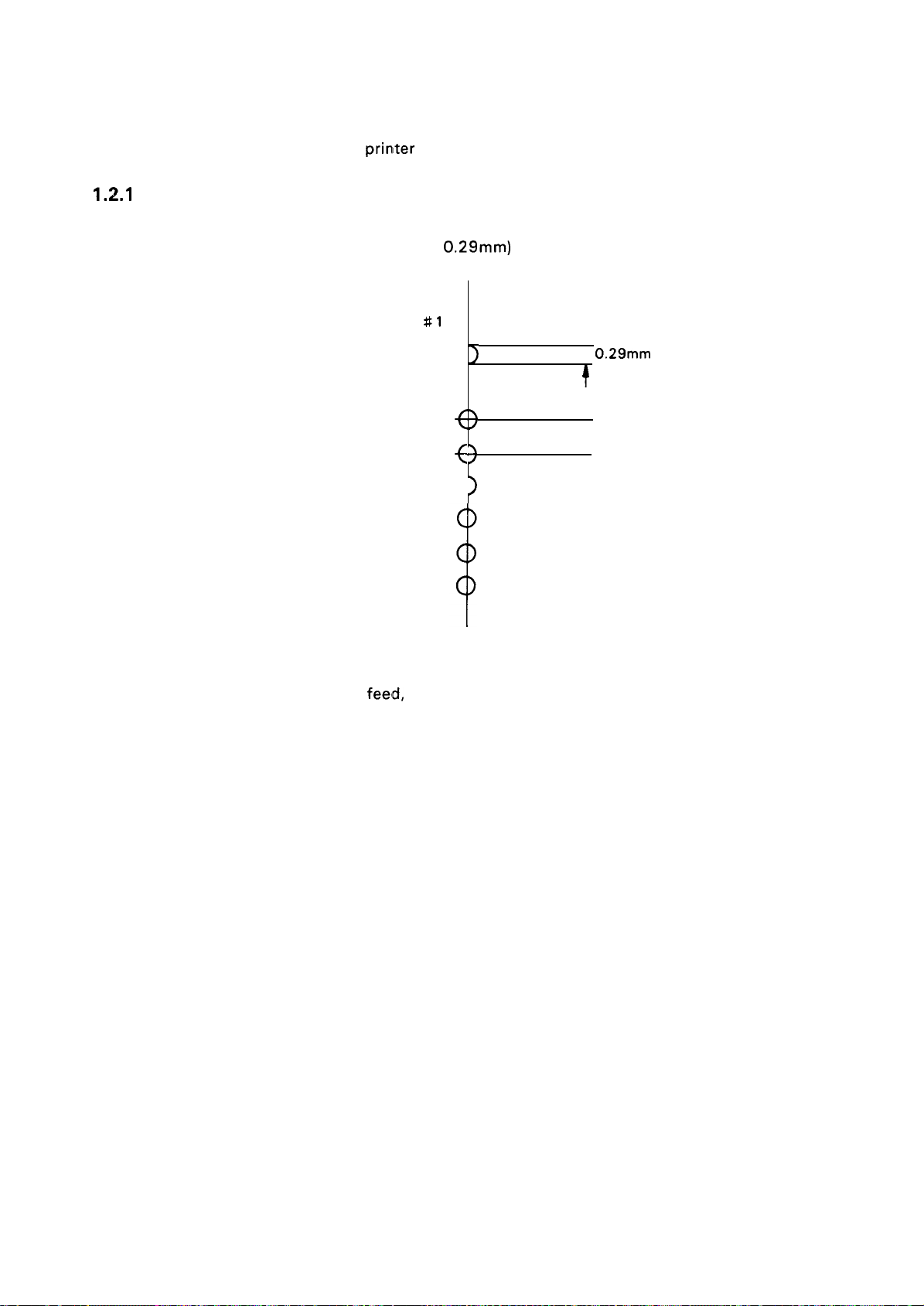
Printing Method
Pin Configuration
Serial, impact, dot matrix
9 wires (diameter
prinlter specifications.
0.29mm)
#1
(
)
#2
(
)
#3
( )
#4
<
>
#5
<
>
#6
(
)
#7
#8
#9
t
0.29mm
!
t
0.35mm (1
f
/72”)
Figure 1-2. Pin Configuration
Feeding Method Friction
When handling paper, note the following precautions described below
Friction Feed Precautions:
1. Do not use continuous paper.
2. Do not use a single sheet shorter than 182mm or longer than
3. Do not perform any reverse paper feed within 8.5mm from the top, or 22mm from the bottom.
4. Do not perform reverse feed greater than 1/6 inch after the paper end is detected.
5. Use the pull-out unit.
6. Do not use multi-part single sheet forms.
Tractor Feed Precautions:
1. Release the friction feed mechanism.
2. Joining of copying paper must be by line or dotted pasting.
3. Copy paper must be a carbon-less, multi-part paper.
feed,
tractor feed (push tractor: standard, pull tractor: optional)
364mm.
1-3
Page 12

REV.-A
a. Push Tractor Feed
1. Use the pull-out unit.
2. Do not perform reverse
3. After paper end detection, accuracy of paper feed cannot be assured and reverse feeding cannot
be performed.
b. Push Pull Feed
1. Remove the pull-out unit and attach the pull tractor unit.
2. Do not loosen the paper between the platen and pull tractor unit.
3. Adjust precisely the horizontal position of the pull and push tractor.
4. Do not perform reverse feeding greater than 1/6 inch.
5. Do not perform reverse feeding after
c. Pull Tractor Feed
1. Remove the pull-out unit and attach the pull tractor unit.
feeding greater than 1/6 inch.
the paper end is detected.
Line Spacing
Paper Insertion
Paper-Feed Speed
Width
Length
Thickness
Si_k&lL
Width
Copies
Quality
Total Thickness
Weight
1/6 inch, 1/’8 inch, or programmable in units of 1/216 inch
From rear
Approximately 95 ins/line (1/6 inch line feeding)
Approximately 75 ins/line (1/6 inch in page feed)
Paper Specifications See Table 1-3 through 1-6
Table 1-3. Cut-Sheet Specifications
182 mm to 257
182 mm to 364 mm (7.15 in. to 14.3 in.)
0.065 mm to 0.14 mm (0.0025 in. to 0.0055 in.)
14 lb. to 24 lb. (52.3 g/mz to 90
mm (7.15 in. to 10.1 in.)
g/m2)
Table 1-4. Continuous Paper Specifications
101 mm to 254 mm (4.0 in. to 10.0 in.)
3 sheets (1 original and 2 copies)
Plain paper
0.065 mm to 0.25 mm (0.0025 in. to 0.01 in.)
1
sheet - 14 lb. to 22 lb., (52.3 g/m2 to 82
3 sheets -- 12 lb. to 15 lb., (40 g/mz to 58.2
g/m2)
g/m2)
each
Table 1-5. Roll Paper Specifications
Width
Weight 14 lb. to 17 lb. (45 kg to 55 kg)
Quality
Thickness
216 mm
Plain paper
0.07 mm to
& 3 mm (8.5 in. & 0.12 in.)
C).09
mm (0.0028 in. to 0.0035 in.)
1-4
Page 13

Table 1-6. Envelope Specifications
REV.-A
NOTES: “
Size
Weight 55Kg (68
Thickness O.19 mm (0.0075 in.) max.
Size
No.6 (166
Imm
x 92 mm), No. 10 (240 mm x 104 mm)
Quality Bond paper, Plain paper, Air mail
Thickness
0.16 mm to
0.52 mm (0.0063 in. to 0.0197 in.)
Difference of thickness within printing area must be less
than 0.25 rnm (0.0098 in.).
Weight 12 lb. to
24
lb. (45 g/m2 to 91 g/m2)
Envelope printing is only available at normal temperature.
.
Keep the long side of the envelope horizontal at setting.
*
Set the left of a
No.6 envelope at the setting mark of the sheet guide.
Table 1-7. Label Specifications
2 1/2 in. X 15/16 in. (63.5 mm X 23.8 mm)
g/m2)
Thickness excluding the base paper must be equal to or less than 0.12
mm (0.0075 in.).
NOTES:
“
Label printing is only available at normal temperature.
● Labels must be a fanfold type.
● For printing labels on pressure sensitive paper, the following conditions must be met: (1)
jointed by dotted or line pasting. (2) total thickness is equal to or less than
inch). (3) 5 degree C to 35 degree C and
10’%0
to
80’ZO
RH.
0.3mm
(0.01 18
1-5
Page 14
REV.-A
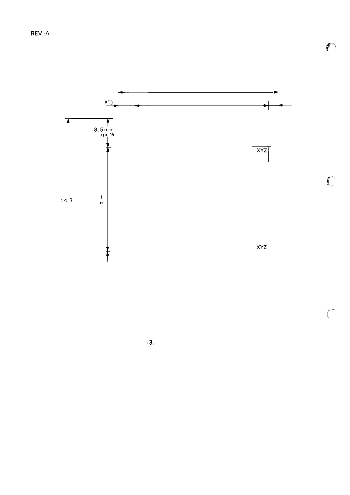
Printing Area
The figures
below show the printing area for cut sheets.
364mm max.
14.3
0.33 “ or
“ max.
182-257 mm(7. 2-10.1 “ )
*1 ) Printable area
4=
8.5rnrY
“e
mt
\
—
—
i
P
r
I
n
t
a
b
I
~
a
r
e
a
ABC
r
-
p)
. .
.
*
*1 )
XYZ
7
,7
““
3../
—
—
● 1 ) At least 3.0 mm (O. 12 in.) when the paper width is less than 229 mm (9 in.); at least 24 mm (0.9
in.) when the paper width is 257 mm ( 10.1 in.)
●
Printing is possible approx. 28 mm from the paper’s detected bottom edge; the 13.5 mm value
(lowest print position) is for reference only. Paper feed accuracy can not be assured within 22 mm
(0.87 in.) of either the top or bottom edge.
ABC
L
Figure 1
—
-:3.
Cut-Sheet Printing Area
XYZ
--l
~.=
~~
1-6
Page 15
REV.-A
Printable
9mm,0.35
or more
9mm,0.35
or
Printable
area
+
“
+
“
mqre
t
area
,101 mm-254mm
Printable area
I
*1)
o
0
0
0
4.0 “ -10.0 “
1A
0
0
0
ABC
0
0
4-
0
0
0
----------------------------0
0
0
0
ABC
0
0
t
0
0
0
0
0
0
1
)(YZ
4
--------------
XYZ
i
I
*2)
I
o
0
0
0
0
0
0
0
0
0
0
0
-0
0
0
0
0
0
0
0
0
0
0
0
● 1) 13 mm or greater for paper widths of 101 - 242 mm (4 - 9.5. in.)
26 mm or greater for paper widths of 254 mm (10 in.)
*2) 13 mm or greater for paper widths of 101 - 242 mm (4 -9.5 in.)
24 mm or greater for paper widths of 254 mm (1 O in.)
Figure 1-4. Printing Area for Continuous Paper
1-7
Page 16
REV.-A
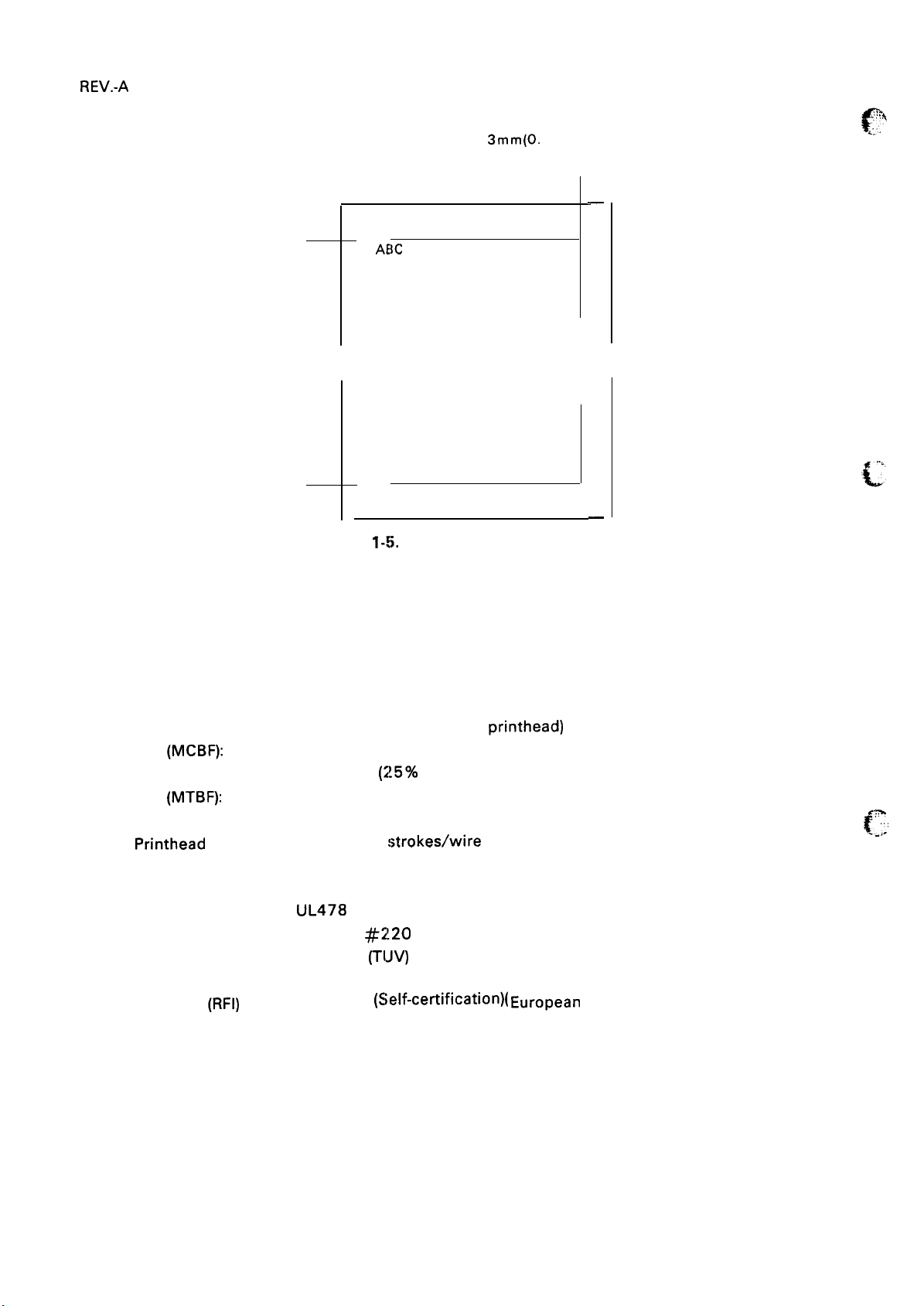
50m
min
60m
I
3rnm min.
‘1
T
1
Figure
2‘1 6mm(8.5 “)*
203.2mm
(printable area)
3mm(0.
I
AEIC
1-3.
Roll Paper Printing Area
12 “ )
3mm min.
XYZ
I
I
—
—
Ink Ribbon
Type:
Color:
Reliability:
Reliability
Mean Cycles Between
Failure
Mean Time Between
Failure
Life of
Safety Approval
Safety Standards
Radio Frequency
Interference
(MCBF):
(MTBF):
Printhead
(RFI)
8750 Ribbon Cartridge
Black
3 million characters at 14 dots/character
3 million lines (excluding printhead)
4000 POH
200 million
UL478
CSA22.2
VDE0806
FCC class B (U.S. version)
VDE 0871
(2!5% duty)
:;trokes\wire
(U.S. version)
#;!20
(Canada version)
(TIJV) (European version)
(Self-certification)(
EurOPean version)
,,
,,:
f-
..
”,.
1-8
Page 17

Electrical Specifications
Power Conditions
Frequency Range
Power Consumption
insulation Resistance
Dielectric Strength
120V Version
220/240V
Version
Environmental Conditions
Temperature
Humidity
Resistance to Shock
Resistance to Vibration
VAC & 10% (120V version)
120
220/240
49.5 to
VAC + 10%
60.!5 Hz
(220/240V
version)
28W (Draft self-test)
10
Mgohms min. (Between AC Line and Chassis)
(At 50 or 60 Hz, between the AC line and chassis)
1 KV AC
1.5KV AC
(rmslminute)
(rms\l
O minutes) or 1250V AC
or 1250V AC
(rms/second)
(rms\second)
5 to 35 degrees C (41 to 95 degrees F) -operating
–30 to 60 degrees C (-22 to 149 degrees F) -storage
10 to 80
5 to 85 %
1 G, within 1
2 G, within 1
YO
RH (no condensation) –operating
FIH
(no condensation) -storage
mS -operating
mS -storage
0.25 G, 55 Hz max. -operating
0.50 G, 55 Hz max. -storage
REV.-A
Physical Specifications
Weight
Dimensions
5.75 Kg
418 mm (Width) X 339 mm (Depth) X 141
excluding knobs and paper guides
mm(Height),
1-9
Page 18
REV.-A
1.2.2
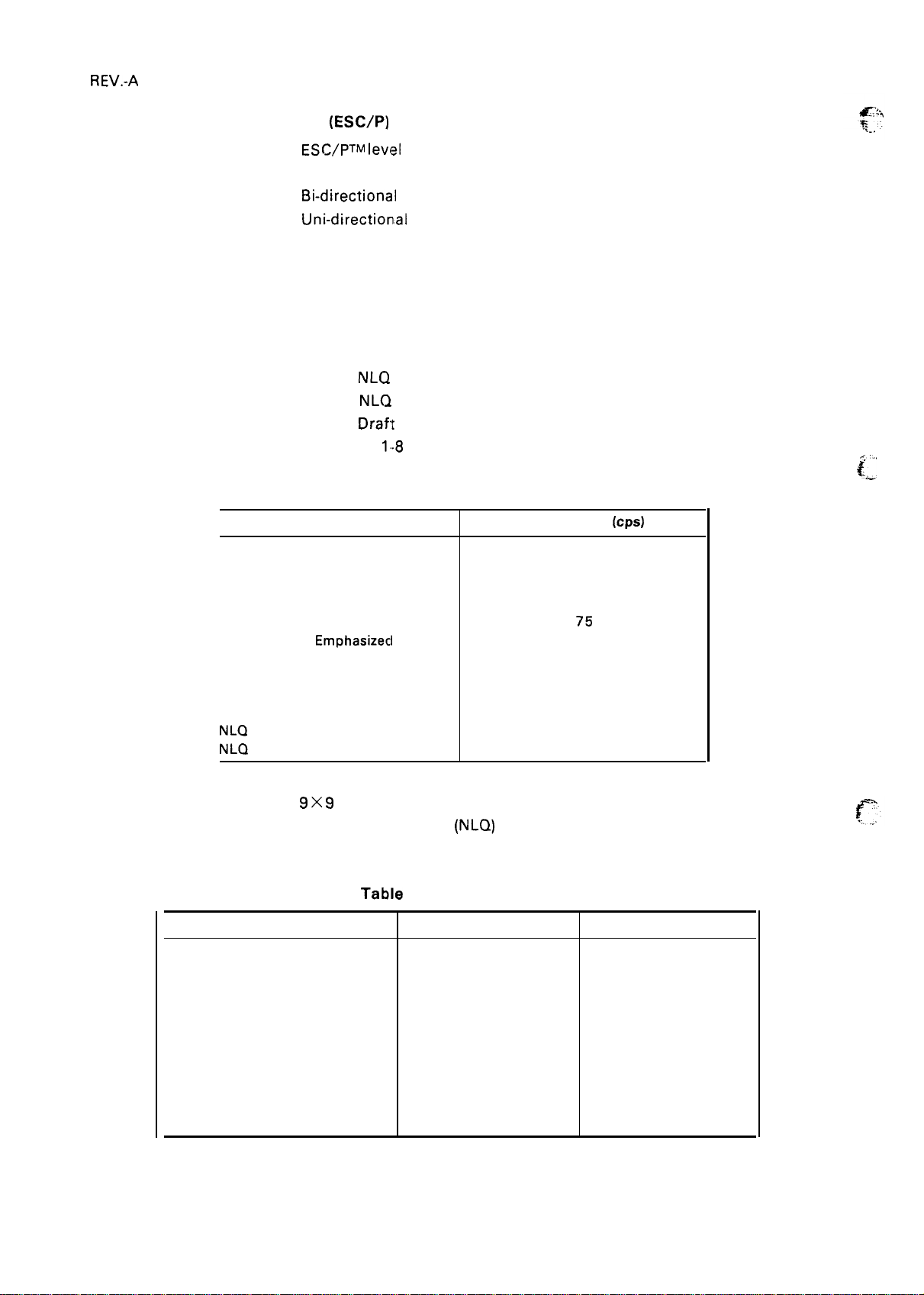
Firmware Specifications
(ESC/P)
Control Code
ESWPTM level ESC/P-81
(EPSON Standard Code for Printers)
Printing Direction
Bi-directional printing with logic seeking (text)
Uni-directional (left to right) printing (Bit-image)
Input data buffer
Character Set
4 K bytes
96 ASCII characters
96 Italic characters
32 International characters (13 countries)
32 International Italic characters
96 IBM Graphics characters
Font
EPSON
EPSON
EPSON
NLQ Roman
NLQ Saris Serif
Draft
Printing Speed See Table
Table 1-8. Printing Speed
Type of Letters
High Speed Draft
Pica
Elite
Double-Width
Emphasized
Double-Width Emphasizecl 37
Condensed
Double-Width condensed
Double-Width Elite
Condensed Elite
NLQ
Pica 25
NLQ
Elite
1.8
Print Speed
200
150
180
75
75
128
64
90
150
30
,,. :.,
{/-.
[cps)
Dot-matrix Format
Character Size
Pica 2.1
Elite
Condensed
Double-Width Pica
Double-Width Elite
Double-Width Condensed 2.1
Condensed Elite
Emphasized
Double-Width Emphasized
Super/Subscript Depends On Pitch
9
X $J Text mode (Draft)
18 X 20 Text mode
See Table 1-9
Type of Letters
(NLQ)
Table 1-9. Character Size
Width (mm)
1.7 3.1
1.05
4.2
3.4
0.85 3.1
2.1
4.2 3.1
1-10
Height (mm)
3.1
3.1
3.1
3.1
3.1
3.1
1.6
Page 19

REV.-A
Printing Columns
Pica
Elite
Condensed
Double-Width Pica
Double-Width emphasized
Double-Width Elite
Double-Width Condensed
(
Condensed Elite
Emphasized
I
See Table 1-10
Table
1-10. Column Width (maximum characters/line)
Type of Letters
Column Width
80
96
137
40
40
48
68
160 20
80
(CPL)
Column/inch
10
12
17
5
5
6
8.5
10
(cpi)
1-11
Page 20
REV.-A
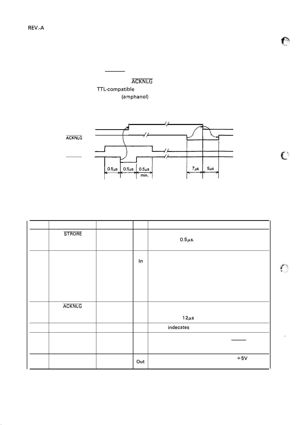
1.3 INTERFACE OVERVIEW
The standard 8-bit parallel interface provided with this printer meets the specifications described below.
Data Format
Synchronization
Handshaking
Signal Level
8-bit parallel
By STROBE pulse
By BUSY and
ACKNLG signal
TTL-compatible
Adaptable Connector 57-30360 (amphanol) or equivalent
Data Transmission Timing See Figure 1-6
/[
BUSY
A
,
{ ,/,, .
ACKNLG
DATA
STROBE
o.5#s
min.
min.
Figure 1-6. Data Transmission Timing
Table 1-11 shows the connector pin assignments and signal functions of the 8-bit parallel interface.
Pin No.
1
2
3
4
5
6
7
8
9
10
11
12
13
Table 1-11. Connector Pin Assignments and Signal Functions
Signal Name
STRORE
DATA 1
DATA 2
DATA 3
DATA 4
DATA 5 24
DATA 6 25
DATA 7
DATA 8
ACKNLG
BUSY
PE
SLCT
Return Pin No. DIR Functional Description
19
20
21
22
23
In
Strobe pulse to read the input data. Pulse width must
0.5,us.
be more than
of this signal.
In
Parallel input data to the printer.
[n
“HIGH” level means data “ 1“.
In
“LOW” level means data “O”.
Input data is latched at falling edge
In
In
In
26
27
In
In
28 out This pulse indicates data is received and ready to
accept next data.
29 out
30 out
Pulse width is
“HIGH”
“HIGH” indicates paper-out.
121.M
indecates
approx.
printer cannot accept next data.
This signal is effective only when ERROR signal is
“LOW”.
—
out
Always
3.3kohms register.)
“HIGH” output. (Pulled up to
+5V
through
1-12
Page 21
Table 1-11. Connector Pin Assignments and Signal Functions (Cont.)
REV.-A
Pin No.
14
Signal Name Return Pin No.
AUTOFEED-XT
15
16
17
Chassis
18
9 to 30
31 I NIT
32
33
34
35
36
Functional Description
feed is
—
DIR
In
if “LOW” when the printer is initialized, a line
automatically performed by input of “CR” code. (Auto
LF)
Not used
GND
GND
— —
Ground for twisted-pair grounding
Chassis ground level of printer
Not used
GND
16
ERROR out “LOW” indicates some error is occurred in the printer.
GND
—
—
—
SLCT-IN
—
Grounds for twisted-pair grounding
50#s
Pulse (Width:
In
initialization.
—
Ground for twisted-pair grounding
—
Not
used
out Always “HIGH”. (Pulled up to
min., active “LOW”) input for printer
+5V
through 3.3 Kohms
register.)
If “LOW” when prinater is initialized, the DC1/DC3
In
control is disabled.
NOTES: 1. “DIR” refers to the direction of the signal flow as viewed from the printer.
2. “Return” denotes a twisted-pair return line.
The cable used must be shielded to prevent noise.
3.
4. All interface conditions are based on TTL levels. Both the rise and fall times of all signals
must be less than 0.2 us.
5. The AUTO FEED-XT signal
6. The SELECT-IN signal can
7. Printing tests, including interface circuit tests, can be performed without using external
equipment by setting DATA 1-8 of the interface connector to certain codes and connecting
the ACKNLG signal to the
c:an
be set LOW by DIP switch 2-4.
ble
set LOW by jumper 1.
STROBE signal.
1-13
Page 22
REV.-A
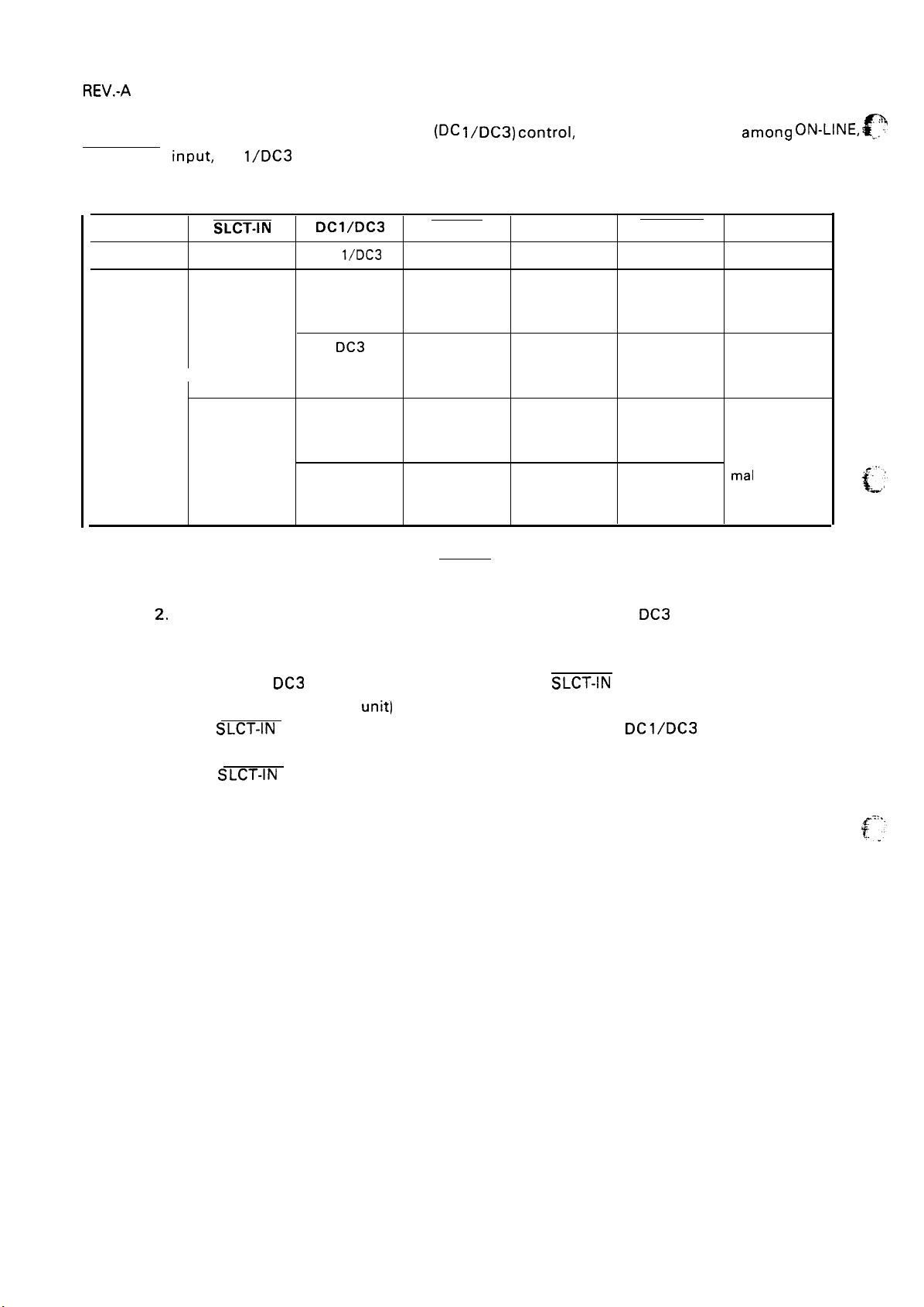
Table 1-12 shows Printer Select/Deselect (DC
SELECT-IN input, DC
l/DC3
and interface signals.
l/DC3)
controL including relations amon9 ON-LINE, .
Table 1-12. Printer Select/Deselect Control
ON-LINE SW
OFF-LINE
ON-LINE
SLCT-IN
HIGH/LOW
HIGH
LOW
Dcl/Dc3
l/DC3
DC
DC 1
DC3
DC 1
DC3 HIGH
ERROR
LOW
HIGH
HIGH
HIGH
BUSY
HIGH
LOW/HIGH
(During data after entry
entry)
LOW/HIGH
(During data after entry
entry)
LOW/HIGH
(During data
entry)
LOW/HIGH
(During data
entry)
ACKNLG
No pulse
Pulse output
Pulse output Enable (Waits
Pulse output
after entry
Pulse output
after entry
DATA ENTRY
Disable
Enable(Normal
Process)
DC 1. See Note
2)
Enable (Nor-
mal
process)
NOTES: 1. In Table 1-12, it is assumed that no ERROR status exists other than that attributable to the
OFF-LINE mode.
2, Once the printer has been put in the deselected state by the DC3 code, the printer will
not revert to the selected state unless the DC 1 code is input again. (In the deselected state,
the printer ignores input data until the DC 1 code is received.)
3. The DC 1 and
for the parallel interface
4. if the
5. If the
SLCT-IN signal is LOW when the printer is initialized,
select control is invalidated, and these control codes are ignored.
SLCT-IN signal is HIGH and is not set to LOW by jumper 1 when the printer is
initialized, the printer starts from the selected (DC 1 ) state.
DC3 codes are enabled only when the SLCT-IN signal (Input Connector No.36
unit) is HIGH and printer power is initialized.
DC1/DC3
printer select/de-
c!
.
1-14
Page 23
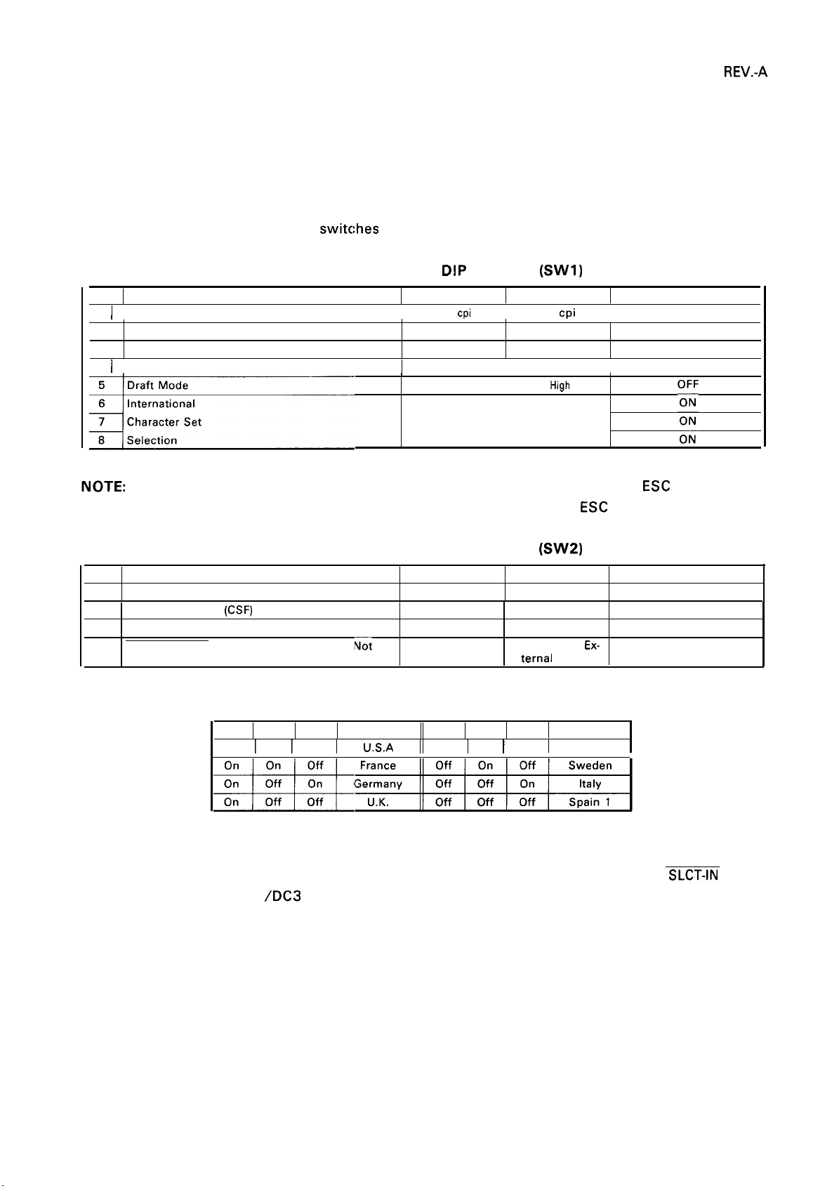
1.4 DIP SWITCH AND JUNIPER SETTINGS
This section describes DIP switch settings for the LX-8 10/850 printer.
1.4.1 DIP Switch Settings
The two DIP switches are located on the side of the printer and function as shown in Tables 1-13 through
1-15. Note that the status of the DIP
switc:hes is read only at power on or upon receipt of the I NIT signal.
Table 1-13. Settings for
No.
1 I Character Pitch
Shape of Zero
2
Table Selection (note)
3
4 I Tear Off
Description
E
When the DIP switch is set for the Italic table, at power on printer defaults to ESC 7 table. When
the switch is set for the Graphic table, at power on it defaults to
Table 1-14. Settings for DIP Switch 2
No.
1
Page length
Cut-Sheet Feeder
2
l-inch skip On
3
4 AUTO FEED XT Signal Internally Fixed or
Description
(CSF)
Mode
.-
~t
D!P
Switch 1
ON
12
I
I
‘
‘
Fixed to LOW
cpi
0
Graphics
Invalid
Normal
See Table 1-15
ON
12 in.
On
(SW1)
OFF
10
I
0
Italics
Valid
I
“gh
(SW2)
OFF
11 in.
off OFF
off
Depends On
ternal Signal
cpi
Fectory Setting
I
I
ESC 6 table.
Factory Setting
Ex-
OFF
OFF
OFF
OFF
:’
OFF
OFF
OFF
Table 1-15. International Character Set Selection
1-6 1-7 1-8
On I On I On
1.4.2 Jumper Setting
Jumper 1 (user-selectable) is located on the TAMA board. If the jumper is connected, the
is fixed to LOW, and DC 1
/DC3
printer select control is ignored.
Country
U.S.A
1-6 1-7
Off ] On I On
1-15
1-8
Country
Denmark 1
SLCT-IN
signal
Page 24

REV.-A
1.5
SELECTYPE
FUNCTION
SelecType
selection of Draft, Roman, or Saris Serif fonts and selection of normal printing or condensed printing
modes.
To select Roman or Saris Serif, press the
When it sounds twice, the Roman font is selected. When it sounds three times, the Saris Serif font is
selected.
To select the Draft font, press the DRAFT button. The buzzer will sound once, indicating that the DRAFT
font is selected.
To set for condensed printing when the printer is in the print mode, press the CONDENSED button once
(the buzzer will sound once), and the printer will enter the condensed print mode.
T
O cancel condensed printing, press the CONDENSED button again. After
buzzer sounds twice to tell you that condensed printing is cancelled.
allows the user to choose fonts and the printing mode easily. This function provides for
SelecType
is effective only when the printer is ON LINE and not printing.
NLQ button. A buzzer sounds when the NLQ button is pressed.
YOU
press the button, the ,. ~
1.6 SHEET LOADING AND SHEET EJECTION
The release lever enables disengaging of the push tractor unit drive mechanism. The printer therefore
provides some improved paper-handling functions through combination of the release-lever and
LOAD/EJECT control panel switch.
,.
‘g,,,
Cut Sheet Loading And Ejection
To load a sheet of paper, position the paper release lever back, place the sheet along the paper guide,
and press the LOAD/EJECT switch. This loads the paper to the top-of-form position.
Pressing the LOAD/EJECT switch after the paper has been loaded will cause the paper to be ejected.
Continuous Paper Loading And Ejection (Back-out)
To load fanfold paper, move the paper release Iever forward, and insert the paper into the push tractor.
~:,
Pressing the LOAD/EJECT switch will then cause paper to be automatically loaded to the top-of-form
position. Pressing the LOAD/EJECT switch after the fanfold paper has been loaded will cause the printer
to eject the paper backward from the push tractor. To back out several pages, press the LOAD/EJECT
switch several times (reverse feed is performed on a page-by-page basis).
ON-LINE LED will flash only when the paper is loaded and the ON-LINE switch pressed. This indicates
The
that the printer has entered “Top-of-form adjust” mode, and that the user may adjust the top-of-form
position, as well as the loading positions for subsequent forms. Adjustment is made using the FORM
FEED button,
which will increment the paper forward, and the LINE FEED switch, which will increment the paper in
reverse. (The minimum feed amount is 2/216 inch).
When cut sheet is used, the adjusted Top-of-form position will be lost when the printer is re-initialized,
and the Top-of from will be reset to the default value. When continuous
memory of the adjusted Top-of-form position will be retained even after
paper is used, however, the
printer initialization.
L.
.,.
1-16
Page 25

REV.-A
1.7 TEAR-OFF
The Tear-Off function
when the release-lever is set to the tractor position. In such a case,
and the printer is
LED will flash to indicate that the FORM FEED and LINE FEED switches are now available to perform
micro-adjustment. The user may then adjust the paper to the tear-off position. This position becomes
the new tear-off position default, and will remain valid even if the printer is reset and reinitialized, and
regardless of whether the main power has been interrupted. When new data are input to the printer,
the paper will automatically be returned to its original position, and printing will then start. Paper having
been advanced to the tear-off position will also be returned to its original position if the ON-LINE switch
is pressed (switching the printer from ON-LINE to OFF-LINE).
FUNCTION
can be enabled by making the appropriate DIP switch setting, and will operate
if the input data buffer is empty
ON-LINIE,
the paper
will
automatically be fed to the tear-off position, and the ON-LINE
1-17
Page 26
REV.-A
1.8 OPERATING INSTRUCTIONS
This section describes the self-test, hexadecimal dump
functions,
error states, printer initialization,
and
buzzer operation.
1.8.1 Self-Test
To begin printing the self-test in the Draft mode, turn the printer ON while pressing the LIN E-FEED button.
To begin printing the self-test using the
it down, then turn the printer power ON.
Self-test printing can be stopped or started by pressing ON-LINE (ON-LINE indicator is not lit). To finish
the self-test, stop the printing by pressing the ON-LINE switch then turn OFF the printer power.
The firmware revision number is printed as the first line of the self-test,
switch settings are printed.
Xxxxxxxx
Character
Shape
CG
Short Tear-off
Draft Print Speed High
Country
Page Length
CSF Mode
Skip Perforation
Auto LF
!
“’P$%&”
#$%&”
$%&”
%&’
&” ( ) *+, -./0 123456789: :
. (
( )%+, -. /0123456789: ; <=>?@ABC
)*+ ,-.
r+,
+ ,- ./0 123456769: ; <=>?
.-./0123456769: ;<=>?@ABCDEFGHIJKMOPQRSmXYZ[\l--`abcdefshijkl~0MrStU-YZ{
-./0123456769:
./0123456789:
/0123456769: ;<=>?@ABCDEFGHIJKIJlNOPQRSTWWX
0123458789: ;<=>?@ABCDEFGHIJKLKNOPQRSTUVWX
123456789: ;<.>?@ABCDEFGHIJKNNOPQRS~~YZ[i]:-=abcdefg~ij~lmopq~etuwyz{ :}-
23458789:
3456789:
456769:
56789:
6789:
769:
89:
9:
:;c.>?9ABCDEFGHIJKUlNOPQRSTUW4XYZ[\] ‘–.abcdefghijklmnopqretuv’wxyz( ;};<=>?@ABCDEFGHIJKl14NOPQRSTtIVWXYZ[\]
<=>?@ABCDKFGHIJK~NOpQRs~
=>?13ABCDEFGHIJKLM?40PQRS
>?@ABCDEFGHIJKLJ4NOpQRSTUVWXYZ[\]
?@ABCDEFGHIJKLllNOPQRSTUVWKY
@ABCDEFGHIJKLMNOPQRSTUVWXYZ[\]
ABCDEFGHIJKLMNOPQRSTUVWX
BCDEFGHIJKLMNOPQRSTUVWXYZ[\l ‘-.
CDEFGHIJKLMNOPQRSTUVWX
DEFGHIJKL4fNOPQRSTW.WKYZ[\l--’abcdefghijklmnopqrstuvwxyz( ;}- !“#$X&-()*+,- ./OlZ34
EFGHIJKLtiNOPQRS’fU%?4X
FGHIJKMINOFQFiSTWWXY
GHIJKLMNOPQESTWWXY
HIJKLHNOPQRSTUVWX
IJKLMNOPQRSTWWXY
JKLM140PQRSTWWKY
KLMNOPQRSTUVWXY
LMNOPQRS1’UWX
MNOPQRSTUV!4X YZ[\]-_” abcdefghijklmnopqretuvwxyz{ 1}NOPQRSTUVWKY
OPQRSTUVWX
PQRSTUVWKYZ[\l -_”abcdefghijklmmopqrotuvwxyz{ ;}QRSTUVWXYZ[\l --’abcdefghijklmnopqrstuvwxyz{ 1}RSTUVWXYZ[\l --’abcdefahlklmnocarstuwxyz(z( !?STUVWXYZ[il:-=abcdefgiiijklmno:a;stuvwxy;{ ~i; !“#ti’()*+,~ .>01234567,
TUVWXYZ[\l --’abcdefghijklmnopZrstuvwxyz{ ;}- !“#w&”()*+,- ./Ol2345678:
WWXYZ[\l
VWXYZ[\]–-’abcdefghijklmnoaratuvwxyz(z( ;}-
Spacing
of Zero
Table
!
“U$%&”
( )*+, -. /0123456789: ; <=>%ABCDEFGHIJKIMNOPQRSTUVWKY
“FF$.%&”
(
)*+,
-. /0123456769: ;
(
)*+,
-. /01234567.99: ;
(
)*+,
- ./0123456769: ;
( )*+, -. /0123456769: ;
( )*+, -. /0123456789: ;
)*+,
-. /0123456769, ;
/o12345678g
-. /012345.5789: ;
;<=>?SIABCDEFGHIJKUINOPQRSTW!4K
;<=>?@ABCDEFGHIJKU!NOP,WS
;<=>?@ABCDEFGHIJKLMNOPQRSTWVWX
:<=>?@ABCDEFGHIJKLtlNOPQESTUVWX
;<=>?@ABCDEFGHIJKLJlNOPQR31’UV!4K
;<=>?@ABcDEFGHIJKLrlNoPQRs17JVw’n
;<.>?@ABCDEFGHIJKLMNOPQRSTUWXYZ[\] “–’abcdefghijklmnopqrstuvwxyz{ t}- !“#3Xd-()
YZ[\l-–’abcdefghijklmnopqr6tu%wxyz{
”_’abcdefghijklmnonratuvwxyz{ 1}-
: ;
<=>?@ABCDEFOmlIJKLMNOPQRSTOVWX
;<=>7@ABCDEFGHIJKLMNOPQRSTUVWXYZ[\l ‘–’abcdefghijklmnopqrstuvwxYz( :
:<=>?@ABCDEFGHIJK~OPQRSWXYZ[\l---abcdefghijklmonrstuwyz( ;}
;<=>?IPABCDEFGHIJKLHN3PQRSTUVWX
Z[\l ”-’abcdefghijklmnopqrc.tuvuxyz( )}- !“#$Xd” ()*.,-./Ol234567
YZ[\l ”-’abcdefghijklmnopqrstuvwxyz( ~}- !-#s%&-OZ+,-
Z[\l--’ abcdefghijklmnopqretuvwxyz( 1}-
Z[\l--’ abcdefghijklmnopqrstuvwxyz( 1}- ?“#sx.4’()*+, -./Ol23456789:
Z[\l-–’abcdefghijklmmopqratuwxyz( !}-
YZ[\]--’abcdefghijklmnopqrstuvwxyz{ ;)-
Z[\]-–’abcdefghijklmnopqratuvwxyz{ :}-
hlLQ
mode (Near Letter Quality), press FORM FEED and hold
and subsequently, current DIP
10 CPI
O
(Unalashed
Italics
Valid
U.S.A.
11 inch
Invalid
None
Depend on I/F
<=>?3ABCDEFOHIJKLMNOPQRS3’WJWX
<=>?6%W,CDEFGHIJKLMNOPQRSTUVWX
<=>?@ASCD8FGHI JKLMNoPQRSTUVWK
<.>?@tABCDEFGHI JKLMNOPQRS’fUVWXYZ
<=>?@ABCDEFGHIJKU4NOPQRSTUVWK
<=>?@ABCDEFGHIJKLMNOPQRSTOVWX
QABCDEFGHIJKLMNOPQRSTUVWXY
YZ[\l--’abcdefghijklmnopqrstuvwxyz( :}- !“#$X&-()*+,
TUTWXYZ[\l --’abcdefghijklmnopqratuvwxyz{ :}- !“#$Xd”()*+,-
Z[\]”-’abcdefghijklmnopqrstuvwxyz( ~}- !“#$xA”()*+,-./
“-.
YZ[\]”-’
YZ[\l--’abcdefghijklmnopqratuvwxyz( ;}- .I’’#$XA ”()*+,-./Ol23
YZ[\l ”–’abcdeft!hi3klmnowr8tuvwxyz{ !)- ?“#sx&-OX+.-. /O12345
Z[<l:_=abcdef~ijklmii~~ituwyz( ~j: r“#$X&”
1-1
)
<=>?@ABCDEFGHIJKLMNOPQRSTUVWX
<=>?@ABCDEFGHIJKMINOPQRSTTJVWX
DEFGHIJKLMNOPQRSTUVWXY
TUVWXYZ[\]--’abcdefghijklmnopqretuvwxyz{ ;}- !“#$
‘–.
‘-.
abcdefghijklmnopqretuwyz(
abcdefghijklmnopqrstuvwxyz{ !}- !“#s%&”OX+,-./Oli?
OFF
1-2 OFF
1-3
oFF
1-4 oFF
1-5 oFF
1-6 ON 1-7 ON 1-6 ON
2-1 OFF
2-2 OFF
2-3 OFF
2-4 OFF
YZ [\
Z [\] ‘-”
YZ[\l
YZ 1 \ 1‘_
Z[\l
YZ[\l-–”abcdefghi$klmnopqretuvwxYz{ ~}-
YZr\l- ‘abcdefghi~klmnopmstuvwwz{ :}-
YZ[\]-–’nbcdefghijklmnopqretuvwxyz{ ;?- !“
YZ[\]-_’abcdefghijklmnopqrstuvwxyz{ ;)- !“#
YZ[\l--abcdefghijklmnopqrotuwyz{
YZ[\l--’abcdef8hijklmnopqretuwxYz{ !}- !“#$Z4
YZ[\l ”–’abcdefghijklumopqrntuvwxYz{ 1}- !“#SXd”
Z[\l-–’abcdefghijklmnopqratuvwxYz{ 1}- !“#$XA’(
abcdefghijklmnopqratuvwxyz{ ;}- !“#SXA”f)*+
abcdefghijklmnopqretuvwxyz{ 1}- !“#$%&”()*+,-.
abcdefghijklmnopqretu..’wxyz{ ;}- ?“#$x&’()*+,-./O
!,,#$x’&-(),+, -./0123456789:;<=>
-
!
;}
!“#$X&-()*+, -./O123456789: ;<=>?@
!“#$Xd’()*+, -./Ol23456789: ;<=>?.9A
!’”#s.&4”()*+. -./Ol23456789:
!-X$X& -()*+.
!“#$X&o (]Jr+,- ./o1234567sg:
Z[\l
‘–’
YZ[\l
YZ[\l‘–“abcdefgbijklmopq
YZC\I ‘-=abcdefg~ijklmmopqr
YZ [\]
YZ [ \ 1‘–
[ \ 1‘–.
]:-yabcdef giij klmnopqratuv
‘-”
abcdef ghl.lklnmopqrstuvwx
abcdefghijklmnopqratuwxY
”
abcdefghijklmnopqretuvwxYz
!“#$x&”
!“#SXd”
()*+.- ./O123456769: ;
!“#$X&-
OX+,-.
! ,,#SX&-OX+,,,#$x&.OX+,- ./OIZ3456789:;<=>?
-./OlZ3456789
abcdefshijklmno
‘-’
abcdefghijklmnop
abcdefghijklmnopqre
abcdef ghij klmnopqrat
abcdefghld klmnopqratu
abcdefghi.lklmnopqratuvw
;}- !“#S.%
{“#S=-()~
1}- !-S$Xd-()*+.-./Ol
()*+,-./Ol23456
./O12345676
()*+,- ./Ol23458789
/OZZ345S789: ;<
./OLZ34567S9:;<=
:<=>?@AB
9:
;<=>WABC
: ;
<=>
;
<=>?W4ECDE
<=>?WBC7DEF
IWABCD
!
i&,””
Figure l-7. Self-Test Printout
1-18
Page 27
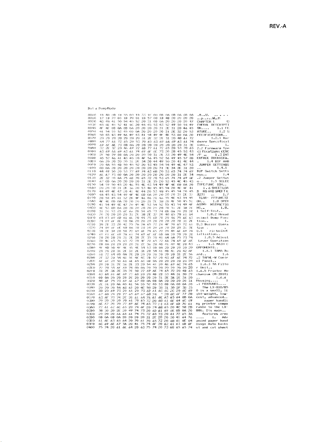
1.8.2 Hexadecimal Dump Function
REV.-A
The printer enters the HEX-DUMP mode when it is powered
on while the LINE-FEED
and FORM-FEED
buttons are pressed down.
the
In the HEX-DUMP mode, the hexadecimal representation of
input data is printed out, along with
corresponding ASCII characters. This function is valuable for checking the data the printer has received
from the host. If input data is a control code rather than a character code, a period (.) is printed in the
ASCII column.
r),<{ ,:! r?,..,.<),,:,
!“IC.,,IC:,
,,($,, ,, IL
“,’.:
,..
,, ,,,,,,, ,., ..,
Clllal,’’rr:.rv
<::~ f:i.c<at,i,cms (1+
/1,,
) ,, .,1.
fYI,r
D I
JE[::
‘11::.AI,V [.)
Al
.I’blr; ‘1’
1.1%, ,. 1.
“ .
I/J.
.,1”1
1, .
.::.:
1,1..IIw
r
[:m.t..
:1. ,, A SIH:::E!:’I
IN!:< {+141) !Wlx r’ K..
1’:l,
(.)11
,...
F’1,” l’,
1.11.1!:: ! :1’
bl!’;’l’F:ll [::’1’T1’)
I...(]fi
:1. .,7
,,0,,
.
(:;
:[i.’r
i. j.
!.,,,
.
,,
L;,,.1
1’,
!’:1.,, ?.(:,,
20
m
f,i::
.
.
[
.
20 6(::
6:?
/,[::
4(:)
<,:1
;.,, O
m
6:1.
‘7:;
:!()
‘7:!
(,2
‘;?:$ 61.;
fi:j
.’!(:
41:,’
61.
61) 61.
<!,8 ‘7.!
’74
fd
7:! ;’?()
Figure 1-8. Hexadecimal Dump Function
.1:,>$ t
,,
1-19
Page 28

REV.-A
1.8.3 Buzzer Operation
The buzzer sounds under the following conditions:
BEL
code:
Carriage trouble:
Paper-out:
Abnormal voltage:
Incorrect RAM:
The buzzer sounds for 0.1 second when a
Beeps 6 times, pausing briefly after 3rd beep.
Beeps 20 times, pausing briefly after every 4 beeps.
Beeps 5 times, pausing after every beep.
(SRAM) Beeps 8 times, pausing briefly after every 2 beeps. (Inside CPU)
Beeps indefinitely until
Recognition of panel operation:
Beeps 1 or 2 or 3 times in setting print mode.
Factory setting:
Sheet ejection failure (in CSF mode):
Illegal paper
releaselunrelease:
Beeps once when the value under micro-adjusting is equal to the
factory-set value.
Beeps 20 times, pausing briefly after every 4 beeps.
Beeps continuously when the paper release lever is changed when the
paper is in the paper path. Beeps until the lever is changed again or the
paper is completely out of the path.
power OFF.
BEL code is input.
.-
$,”.
.*
1-20
Page 29
REV.-A
1.8.4 Printer Initialization
The printer is initialized when:
1 ) AC power is turned on
2) The INIT signal is input
Here is a brief summary of the initialization sequence.
a)
Return the printhead to the Ieftmclst position.
b)
Set ON LINE mode.
c)
Clear the print buffer and input buffer.
d)
Set the line spacing to 1/6 inches.
e)
Set the page length to 11 or 12 inches according to the DIP switch setting.
Clear all vertical tab positions.
f)
Set the horizontal tab position at 13-column intervals.
9)
h)
Set the print mode according to tlhe DIP switch setting and the non-volatile memory setting of
the control panel.
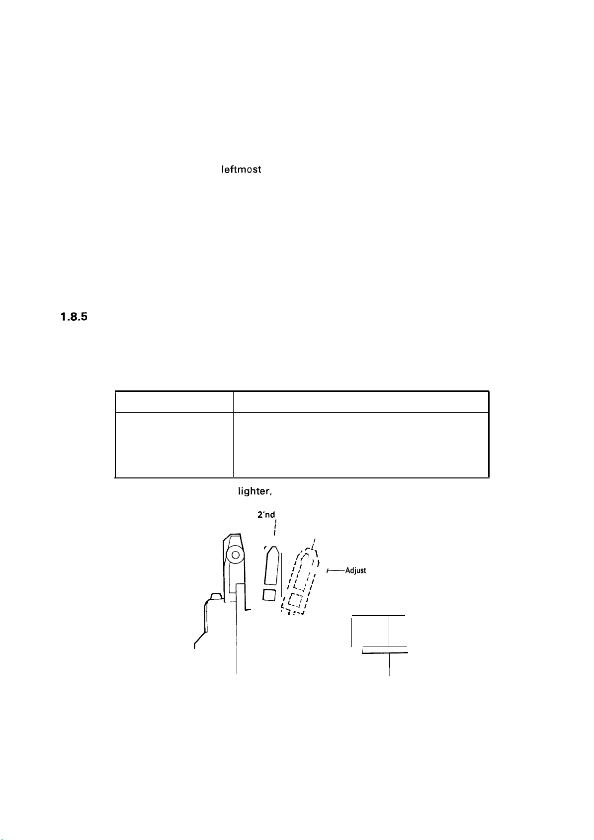
1.8.5
Adjust Lever Operation
The adjust lever must be set to the proper position according to the paper of paper you are using. Refer
to Table 1-16 and Figure 1-9 below.
Table 1-16. Lever Position
~Adjust
Paper
Lever
Lever Position
2nd step
3rd step
4th step
4th to 7th step
● If printing density becomes Ii!ghter, set the adjust lever position one step narrower.
F
Cut sheet, continuous paper (non copy, 1 + 1 copy)
Continuous paper (1 +2 copies)
Label
Envelope
2’ndl
position
4’th position
m
o
/
f;’-’
t, )}
II
o
I
<.41 I
I
l..
u
““~
l’.
$..;/’
pi,
/
~“
‘
L
I
7
Figure 1-9. Lever Position
1-21
Page 30
REV.-A
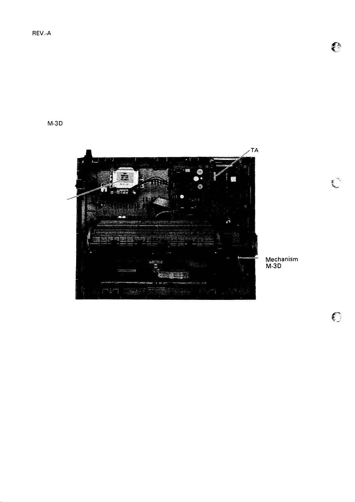
1.6 MAIN COMPONENTS
The main components of the LX-8 10/850 printer are designed for easy removal and replacement to
maintain/repair the printer.
The main components are:
1 ) TAMA board: Main control board. The CPU on this board controls all main functions.
2) TAPNL-W control panel: Control panel.
3) TA filter unit: Transformer and filter board.
M-3D 10: Printer mechanism.
4)
MA board
TA
Filter
Unit
. . .
t..
Figure 1-10. 1.X-81 0/850 Component Layout
Printer
—
Mechanis
M-3D
10
1-22
Page 31

1.6.1 TAMA Board
REV.-A
The use of the
~PD78
10HG CPU simplifies the main control board circuit design.
. PROM (3C)
(3D)
-SRAM
Gate Array
E05430 (3B)
- CPU
LPD78 10HG
(2C)
1.6.2
The
TAPNL-W
switches.
TAPNL-W
control panel is the LX-8 10/850 control panel which contains the indicator LEDs and
Figure 1-II 1.
Control Panel
Figure
TAMA
1-12.
TAPNL-W Control Panel
Main Control Board
1-23
Page 32

REV.-A
1.6.3
TA Filter Unit
The TA filter unit contains a power cord ( 120V Version) or AC inlet
fuse, filter circuit, and power transformer.
(220V
(120V Version)
Version)
Figure 1-13. TA Filter Unit
1.6.4 Printer Mechanism (M-3D1O)
The M-3D 10 printer mechanism was developed specifically
include:
Carriage motor
Carriage mechanism
Paper feed motor
Paper feed mechanism
Ribbon feed mechanism
Printhead
Sensors
for the LX-8 10/850 printer. Its components
(220/240V
(240V
Version), power switch
Version)
Figure 1-14. Nlodel-3Dl O Printer Mechanism
1-24
-.
Page 33

REV.-A
1.6.5 Housing
The LX-8 10/850 housing consists of the upper and lower cases. The upper case houses the control
panel. The lower case houses the printer mechanism and the main control board.
f:igure
1-15. Housing
1-25
Page 34

CHAPTER 2
PRINCIPLES OF OPERATION
REV.-A
2.1
OVERVIEW
2.1.1 Connector Summary
2.1.2 Outline of Printer Mechanism Operation . . . . . . . . . . . . . . . . . . . . . . 2-3
2.1.3 Circuit Overview
2.2
PRINCIPLES OF OPERATION
2.2.1 Power Supply Circuit . . . . . . . . . . . . . . . . . . . . . . . . . . . . . . . . . . . . . . . . . . . . . . . . . . . . . . . . . .
2.2.2 Reset Circuit
2.2.3 Carriage Operation
. . . . . . . . . . . . . . . . . . . . . . . . . . . . . . . . . . . . . . . . . . . . . . . . . . . . . . . . . . . . . . . . . . . . . . . . . . . . . . . . . . . . . . . . . . . . .
. . . . . . . . . . . . . . . . . . . . . . . . . . . . . . . . . . . . . . . . . . . . . . . . . . . . . . . . . . . . .
2.1.2.1 Sensors
2.1.2.2
2.1.2.3
2.2.1.1 TA Filter Unit . . . . . . . . . . . . . . . . . . . . . . . . . . . . . . . . . . . . . . . . . . . . . . . . . . . . . . .
2.2.1.2 + 12V DC Power Supply Circuit . . . . . . . . . . . . . . . . . . . . 2-12
2.2.1.3
2.2.1.4 +5A/ DC Power Supply Circuit . . . . . . . . . . . . . . . . . . . . . . . 2-19
2.2.2.1 Power-on Reset
2.2.2.2 Operation at Reset
2.2.2.3 Power-off Reset
Mc~tors
Printhead
. . . . . . . . . . . . . . . . . . . . . . . . . . . . . . . . . . . . . . . . . . . . . . . . . . . . . . . . . . . . . . .
+2!4V
DC Power Supply Circuit . . . . . . . . . . . . . . . . . . . . 2-13
. . . . . . . . . . . . . . . . . . . . . . . . . . . . . . . . . . . . . . . . . . . . . . . . . . . . . . . . . . . . . . . . . . . .
. . . . . . . . . . . . . . . . . . . . . . . . . . . . . . . . . . . . . . . . . . . . . . . . . . . . . . . . . . . . . . . . . . . . .
. . . . . . . . . . . . . . . . . . . . . . . . . . . . . . . . . . . . . . . . . . . . . . . . . . . . . . . . . . . . . . . . . . . .
. . . . . . . . . . . . . . . . . . . . . . . . . . . . . . . . . . . . . . . . . . . . . . . . . . . . . . . . . .
. . . . . . . . . . . . . . . . . . . . . . . . . . . . . . . . . . . . . . . . . . . . . . . . . . . . . . . . . . . . . . . . . . . . . . . . . . .
. . . . . . . . . . . . . . . . . . . . . . . . . . . . . . . . . . . . . . . . . . . . . . . . . . . .
. . . . . . . . . . . . . . . . . . . . . . . . . . . . . . . . . . . . . . . . . . . . . .
. . . . . . . . . . . . . . . . . . . . . . . . . . . . . . . . . . . . . . . . . . . . . . . . . . .
. . . . . . . . . . . . . . . . . . . . . . . . . . . . . . . . . . . . . . . . . . . . . . . . . . . . . . . . . . . . . . . .
2-1
2-1
2-4
2-7
.
2-7
2-8
2-10
.
2-10
.
2-11
2-20
2-20
2-21
2-21
2-22
2.2.3.1 Carriage Mechanism . . . . . . . . . . . . . . . . . . . . . . . . . . . . . . . . . . . . . . . . . . 2-22
2.2.3.2 Carriage Motor Specification
2.2.3.3 Carriage Motor Drive Circuit
Block Diagram
2.2.3.4 Carriage Motor Drive Circuit
2.2.3.5 Carriage Motor Software Control ................. 2-32
2.2.4 Paper Feed
2.2.4.1 Paper Feed Mechanism Operation ................ 2-35
2.2.4.2 Paper-Feed Motor Specifications ................... 2-36
2.2.4.3 Paper-Feed Motor Drive Circuit . . . . . . . . . . . . . . . . . . . . . . 2-37
2.2.4.4 Paper-Feed Motor Software Control ............. 2-38
2.2.5
Printhead
2.2.5.1
2.2.5.2
2.2.5.3
2.2.5.4 Gate Array E05A30 Operation in
Printhead
Printhead
Printhead
Drive Circuit . . . . . . . . . . . . . . . . . . . . . . . . . . . . . . . . . . . . . . . . . . . . . . . . . . . . . . . . .
. . . . . . . . . . . . . . . . . . . . . . . . . .
. . . . . . . . . . . . . . . . . . . . . . . . . . . . . . . . . . . . . . . . . . . . . . . . . . . . . .
. . . . . . . . . . . . . . . . . . . . . . . . . . .
. . . . . . . . . . . . . . . . . .
. . . . . . . . . . . . . . . . . . . . . . . . . . . . . . . . . . . . . . . . . . . . . . . . . . . . . . . . . . . . . . . . . . . . . . . . . . . . . . . . . .
.
. . . . . . . . . . . . . . . . . . . . . . . . . . . . . . . . . . . . . . . . . . . . . . . . . . . . . . . . . . . .
Printing Operation
Specification
Drive Circuit Block Diagram ....... 2-40
. . . . . . . . . . . . . . . . . . . . . . . . . .
. . . . . . . . . . . . . . . . . . . . . . . . . . . . . . . . . . . . .
Printhead
2-22
2-23
2-24
2-35
2-39
2-39
2-39
.
2-40
2-i
Page 35

REV.-A
2.2.5.5
2.2.5.6
2.2.6 Host Interface . . . . . . . . . . . . . . . . . . . . . . . . . . . . . . . . . . . . . . . . . . . . . . . . . . . . . . . . . . . . . . . . . . . . . . . .
2.2.7 EEPROM Circuit . . . . . . . . . . . . . . . . . . . . . . . . . . . . . . . . . . . . . . . . . . . . . . . . . . . . . . . . . . . . . . . . . . . .
2.2.8 Ribbon-Feed Mechanism
Printhead
Printhead
Software Control . . . . . . . . . . . . . . . . . . . . . . . . . . . . 2-42
Drive Circuit
. . . . . . . . . . . . . . . . . . . . . . . . . . . . . . . . . . . . . . . . . . . . . . . . . . . . .
. . . . . . . . . . . . . . . . . . . . . . . . . . . . . . . . . . . . .
2-41
.
2-44
.
2-45
2-46
LIST OF FIGURES
Figure 2-1.
Figure 2-2.
Figure 2-3.
Figure 2-4.
Figure 2-5.
Figure 2-6.
Figure 2-7.
Figure 2-8.
Figure 2-9. Printhead
Figure 2-10. TAMA Board Block Diagram
Figure 2-11. Power Supply Circuit Block Diagram
Figure 2-12. Transformer Circuit
Figure 2-13. + 12V DC Power Supply Circuit . . . . . . . . . . . . . . . . . . . . . . . . . . . . . . . . . . . . . . .
Figure 2-14.
Figure 2-15. Rectifier and Smoothing Circuit
Figure 2-16.
Figure 2-17. Voltage Feedback Circuit
Figure 2-18. Over-Current Protection Circuit
Figure 2-19. Output Transistor Drvie Waveform
Figure 2-20. Chopping Circuit . . . . . . . . . . . . . . . . . . . . . . . . . . . . . . . . . . . . . . . . . . . . . . . . . . . . . . . . . . . . . . . . . . .
Figure 2-21.
Figure 2-22. Reset Circuit
Figure 2-23. RESET Output . . . . . . . . . . . . . . . . . . . . . . . . . . . . . . . . . . . . . . . . . . . . . . . . . . . . . . . . . . . . . . . . . . . . . . . .
Figure 2-24. Carriage Mechanism . . . . . . . . . . . . . . . . . . . . . . . . . . . . . . . . . . . . . . . . . . . . . . . . . . . . . . . . . . . .
Figure 2-25. Carriage Drive Circuit Block Diagram . . . . . . . . . . . . . . . . . . . . . . . . . . . . 2-23
Figure 2-26. Carriage
Figure 2-27. SLA 7020M Circuit Diagram . . . . . . . . . . . . . . . . . . . . . . . . . . . . . . . . . . . . . . . . . . . . . 2-25
Figure 2-28. Phase Data Input Circuit (2-2 Phase) . . . . . . . . . . . . . . . . . . . . . . . . . . . . . 2-26
Figure 2-29. Phase Signal Timing Chart (2-2 Phase) . . . . . . . . . . . . . . . . . . . . . . . . . 2-26
Figure 2-30. Phase Data Input Circuit (l-2 Phase) . . . . . . . . . . . . . . . . . . . . . . . . . . . . . 2-27
Figure 2-31. Phase Signal Timing Chart (l-2 Phase) . . . . . . . . . . . . . . . . . . . . . . . . . 2-27
Figure 2-32. Reference Voltage Generation Circuit . . . . . . . . . . . . . . . . . . . . . . . . . . . 2-28
Figure 2-33. Constant Current Control Circuit . . . . . . . . . . . . . . . . . . . . . . . . . . . . . . . . . . . . 2-29
Figure 2-34. Waveforms . . . . . . . . . . . . . . . . . . . . . . . . . . . . . . . . . . . . . . . . . . . . . . . . . . . . . . . . . . . . . . . . . . . . . . . . . . . . . .
Figure 2-35. Carriage Motor Control . . . . . . . . . . . . . . . . . . . . . . . . . . . . . . . . . . . . . . . . . . . . . . . . . . . . . .
Cable Connections . . . . . . . . . . . . . . . . . . . . . . . . . . . . . . . . . . . . . . . . . . . . . . . . . . . . . . . . . . . . . . . .
Printer
Paper-End
Paper-End Sensor
Home-Position Sensor Mechanism . . . . . . . . . . . . . . . . . . . . . . . . . . . . . . . . . . 2-5
Home-Position Sensor Circuit
Release Sensor Mechanism
Release Sensor Circuit . . . . . . . . . . . . . . . . . . . . . . . . . . . . . . . . . . . . . . . . . . . . . . . . . . . . . . . .
+24V
DC Power
+24DC
+5V
Mechi~nisrn
Sensor Mechanism . . . . . . . . . . . . . . . . . . . . . . . . . . . . . . . . . . . . . . . . . . . 2-4
. . . . . . . . . . . . . . . . . . . . . . . . . . . . . . . . . . . . . . . . . . . . . . . . . . . . . . . . . . . . . . . . . . . . . . . . . . . . . . . . . .
SupPly
Circuit . . . . . . . . . . . . . . . . . . . . . . . . . . . . . . . . . . . . . . .
Switching Regulator Circuit
DC Power Supply Circuit
Motor
Drive Circuit . . . . . . . . . . . . . . . . . . . . . . . . . . . . . . . . . . . . . . . . . . . . . 2-24
Block Diagram
Circuit . . . . . . . . . . . . . . . . . . . . . . . . . . . . . . . . . . . . . . . . . . . . . . . . . . .
. . . . . . . . . . . . . . . . . . . . . . . . . . . . . . . . . . . . . . . . . . . . . . .
. . . . . . . . . . . . . . . . . . . . . . . . . . . . . . . . . . . . . . . . . . . . .
. . . . . . . . . . . . . . . . . . . . . . . . . . . . . . . . . . . . . . . . . . . . . . . . . . . . . . . . . . . . . . .
. . . . . . . . . . . . . . . . . . . . . . . . . . . . . . . . . . . . . . . . . . . . . . . . . . . .
. . . . . . . . . . . . . . . . . . . . . . . . . . . . . . . . . . . . . . . . . . . . . . . . . . . . . . . . . . . . . . . . . . . . . . . . . . . .
. . . . . . . . . . . . . . . . . . . . . . . . . . . . . . . . .
. . . . . . . . . . . . . . . . . . . . . . . . . . . . . . . . . . . . . . . . . . . .
. . . . . . . . . . . . . . . . . . . . . . . . . . . . .
. . . . . . . . . . . . . . . . . . . . . . . . . . . . . . . . . . . . . . .
. . . . . . . . . . . . . . . . . . . . . . . . . . . . . .
. . . . . . . . . . . . . . . . . . . . . . . . . . . . . . . . . . . . . . . .
. . . . . . . . . . . . . . . . . . . . . . . . . . . . . . . .
. . . . . . . . . . . . . . . . . . . . . . . . . . . . . . . . . . . . . . . . .
.
2-2
2-3
.
2-4
2-5
2-6
.
2-6
2-7
2-8
2-10
2-11
2-12
2-13
2-13
2-14
2-15
2-16
2-17
. 2-18
2-19
2-20
. 2-20
.
2-22
. 2-30
.
2-33
p
.., ,.,
,,, ,
Z.ii
Page 36

REV.-A
Figure 2-36.
Figure 2-37.
Figure 2-38.
Figure 2-39.
Figure 2-40.
Figure 2-41.
Figure 2-42.
Figure 2-43.
Figure 2-44.
Figure 2-45.
Figure 2-46.
Figure 2-47.
Figure 2-48.
Figure 2-49.
Figure 2-50.
Figure 2-51.
Home-PositionSeak . . . . . . . . . . . . . . . . . . . . . . . . . . . . . . . . . . . . . . . . . . . . . . . . . . . . . . . . . . . . .
Printing Area and Printing Timing
Friction-Feed Operation . . . . . . . . . . . . . . . . . . . . . . . . . . . . . . . . . . . . . . . . . . . . . . . . . . . . . .
Push Tractor Feed Operation
Paper-Feed Motor Drive Circuit
Paper-Feed Motor Drive Timing Chart
Printhead
Printing Operation . . . . . . . . . . . . . . . . . . . . . . . . . . . . . . . . . . . . . . . . . . . . 2-39
Printhead
Printhead
Printhead Driving
Print Timing . . . . . . . . . . . . . . . . . . . . . . . . . . . . . . . . . . . . . . . . . . . . . . . . . . . . . . . . . . . . . . . . . . . . . . . . . . . .
A/D Converter
Relationship between Head Driver Voltage and
Print Driving Pulse Width . . . . . . . . . . . . . . . . . . . . . . . . . . . . . . . . . . . . . . . . . . . . . . . . .
Host Interface
EEPROM Circuit . . . . . . . . . . . . . . . . . . . . . . . . . . . . . . . . . . . . . . . . . . . . . . . . . . . . . . . . . . . . . . . . . . . .
Ribbon-Feed Mechanism
Drive Circuit Block Diagram . . . . . . . . . . . . . . . . . . . . . . . . . 2-40
Drive Circuit . . . . . . . . . . . . . . . . . . . . . . . . . . . . . . . . . . . . . . . . . . . . . . . . . . . . . . .
Waveforms
(+24V
. . . . . . . . . . . . . . . . . . . . . . . . . . . . . . . . . . . . . . . . . . . . . . . . . . . . . . . . . . . . . . . . . . . . . . . . .
VDC Line Monitor) Circuit ..... 2-42
. . . . . . . . . . . . . . . . . . . . . . . . . . . . . . . . . . . . . . . . . . . . . . . . . . . . . .
. . . . . . . . . . . . . . . . . . . . . . . . . . . . . . . . . .
. . . . . . . . . . . . . . . . . . . . . . . . . . . . . . . . . . . . . . . . . . . .
. . . . . . . . . . . . . . . . . . . . . . . . . . . . . . . . . . . . . . . .
. . . . . . . . . . . . . . . . . . . . . . . . . . .
. . . . . . . . . . . . . . . . . . . . . . . . . . . . . . . . . . . . . . . . . . .
.
2-33
2-34
.
2-35
2-36
2-37
2-38
.
2-47
2-41
.
2-42
.
2-43
2-44
.
2-45
2-46
LIST OF TABLES
Table 2-1.
Table 2-2.
Table 2-3.
Table 2-4.
Table 2-5.
Table 2-6.
Table 2-7.
Table 2-8.
Board Connecl:or Summary
Voltage Applications . . . . . . . . . . . . . . . . . . . . . . . . . . . . . . . . . . . . . . . . . . . . . . . . . . . . . . . . . . . . . . . .
Reference
Phase-Excitation Method . . . . . . . . . . . . . . . . . . . . . . . . . . . . . . . . . . . . . . . . . . . . . . . . . . . . . . . .
Drive Sequence (2-2 Excitation . . . . . . . . . . . . . . . . . . . . . . . . . . . . . . . . . . . . . . . . . . . . . 2-32
Drive Sequence (l-2 Excitation) . . . . . . . . . . . . . . . . . . . . . . . . . . . . . . . . . . . . . . . . . . . . 2-32
Excitation Sequence (Clockwise : Paper Feeds
Forward)
Ribbon-Feed Gear Train . . . . . . . . . . . . . . . . . . . . . . . . . . . . . . . . . . . . . . . . . . . . . . . . . . . . . . . . . . .
Voll:age
. . . . . . . . . . . . . . . . . . . . .
. . . . . . . . . . . . . . . . . . . . . . . . . . . . . . . . . . . . . . . . . . . . . . . . . . . . . . . . . . . . . . . . . . . . .
.
. . . . . . . . . . . . . . . . . . . . . . . . . . . . . . . . . . . . . . . . . . . . . . . . . . . . . . . . . . . . . . . . . .
. . . . . . . . . . . . . . . . . . . . . . . . . . . . . . . . . . . . . . . . . . . . . . . . . . . .
2-1
. 2-10
2-28
.
2-32
2-38
.
2-46
Z.iii
Page 37

REV.-A
2.1 OVERVIEW
This chapter describes the signals at the connectors linking the primary components of the LX-8 10/850.
These components include the printer mechanism and control circuits. The chapter also describes the
operation of the printer’s circuitry and
2.1.1 Connector Summary
The interconnection of the primary components is illustrated in Figure 2-1. Table 2-1 summarizes the
functions, sizes, and types of the connectors shown in the figure.
Table 2-’1. Board Connector Summary
/printer mechanism.
Board
TAMA
Board
Connector
CN
1
CN2
CN3
CN4
CN5
CN6
CN7
CN8
CN9
CN 10
Function
Host l/F (Parallel)
Optional I/F
Control Panel
Release Lever
CR Motor and PF Motor
PE Signal
Home Position Signal
Head
AC Power Input
DC Power Input (OEM)
:
Board
Pins
36 1-11
26 A-8
10
2
12
2
2 A-13
12
4
4
Reference Table
A-9
A-1 O
A-1 1
A-12
A-1 4
A-15
A-16
2-1
Page 38

REV.-A
FiiEElr
Board
Control
Panel
Model 3D 10 Printer Mechanism
Release
CR motor
PF motor
PE
HOME
HEAd
—
,
1 OPin
2Pin
TAMA Board
12Pin
2Pin
c
:
.5
: 5
co
ii~
-u
n
.5
L
-
36 Pin
m
L
J
Paralel
l/F
c
m ,-
zn
“:
n
[
Optional l/F
)
‘1
Optional
Interface
Board
l-l
I
Parallel l/F j Specific l/F
l----------~ ----------i
HOST COMPUTER
I
I
I
II
E
5
co
m
z
u
Power Input I
(OEM)
I
TA Filter
r–––––––n
I
Transformer
I
I
I
/\
I
I
Filter
I
Board
I
I
t:
I
L
AC”IN
Unit
“’?
,.
L’
I
1
I
1
‘
~-..
., .,..,.
NOTE: CR = carriage.
PF = paper feed.
HP = home position.
PE = paper end.
Figure 2-1. Cable Connections
2-2
Page 39

REV.-A
2.1.2 Outline of Printer Mechanism Operation
Model 3D 10 is a 9-pin serial dot matrix printer. Because the frame and many of the components
The
are of plastic, the mechanism is lightweight. A block diagram of the printer mechanism is shown in
Figure 2-2.
&
z
w
f
5:
:: :
U
m
$
A
u
a
~.:
(0
--(>
NE
=0
0+
Ku
v<
~~
u
1
~
2’:
$.:
~:
$
.-
CW = clockwise; CCW= counterclockwise.
HP = home position; PE= paper end.
Figure 2-2. Printer Mechanism Block Diagram
2-3
Page 40

REV.-A
“.. .
~.
,-
2.1.2.1 Sensors
The printer mechanism is equipped with the following sensors:
Paper-End
Home-Position (HP) Sensor
Friction/Tractor Sensor
(PE)
Sensor
Paper-End Sensor
Figures 2-3 and 2-4 show the paper-end sensor. This sensor switch is ON when no paper is in place
(e.g., when the paper supply has run out).
“Paper-out”
Paper present
(PE
~
ON ~ LOW
~
OFF + HIGH
sensor)
~Jq~
o
/
‘“Paper-out”
Platen
Paper guide
Paper-End Sensor
/
Paper
o
c~
/
“Paper present”
Figure 2-3. Paper-End Sensor Mechanism
+5V
&&.
7A’
Figure 2-4. Paper-End Sensor Circuit
R96
IK
2-4
Page 41

REV.-A
Home-Position Sensor (HP sensor)
Figures 2-5 and 2-6 show the home-position sensor. The sensor switch is ON when the carriage is at
the home position.
Home position + ON
Other positions + OFF - HIGH
This sensor determines the reference
-+
LOIA/
pcxsition
for the carriage drive,
age guide
iage
shaft
Figure 2-5. Home-Position Sensor Mechanism
+5V
4
CN7-1
<o—————u
R97
IK
J
Figure 2-6. Home-Position Sensor Circuit
-
HOME
2-5
Page 42

REV.-A
Friction/Tractor Sensor
The release sensor senses the position of the release lever in order to detect whether tractor feed or
friction feed is in effect.
Release Lever Position : Front + F:riction Feed + OFF + HIGH level
Release Lever Position : Rear -+ Tractor Feed ~ ON ~ LOW level
:$-2!
+.
Front
\
?“’”-
\ i,
\
~.
<
~
Figure 2-7’.
Rear
/
ease
Lever
w
Friction/Tractor Sensor
Release Sensor Mechanism
+5V
4
r’
oJKL-=
R95
IK
Figure
:2-8.
Release Sensor Circuit
2-6
Page 43

REV.-A
2.1.2.2 Motors
This printer has the following motors:
Carriage motor (step motor)
Paper-feed motor (step motor)
Carriage Motor
The carriage motor is used to move the carriage right and left along the platen. This unit employs a
4-phase, 48-step motor using either 1-2
Paper-Feed Motor
Paper feed is also driven by a 4-phase 48-step motor operating with 2-2 phase excitation. Each phase
switch causes the paper to advance by advanced 1/2 16“ for each phase switch. The gate array controls
the motor through an open loop.
or 2-2
Phase excitation.
An
open-loop system is Used for control.
2.1.2.3
Figure 2-9 shows the dot-wire operation.
When the head-driving coil is energizecl, the dot wire is pushed out. The dot wire strikes the ribbon,
causing the ribbon to impact the paper, thereby printing a dot.
Printhead
/Ribbon
Platen
Dot
‘Core
Figure 2-9.
Printhead
2-7
Page 44

REV.-A
2.1.3 Circuit Overview
h,
,.
f.
Figure 2-10 shows a block
--7rmm
ADDRESS
i
PD78 10HG
(2 c)
EEPROM
(1 c)
B
XWl
DATA/ADDRESS BUS (LOWER BYTE)
~Q=
,LE
J
‘Usir+km+=l
diagram of the TAMA board circuitry.
PROM
32KB
r
BUS
(UPPER
ADDRESS
LATCH
(3C)
BYTEI
I
GA E05A30 (36)
RAM
8KB/32KB
h
A[)DRESS
DECODER
‘3”)’
CONTROL PANEL
I
CONTROL PANEL
LED DRIVE
I
24VDC +5VDC + 12vDC
+
t
t
t,
CG = character generator; GA = gate array.
Figure 2-10.
The circuit consists mainly of the following
● ~PD7810HG CPU (2C)
The
~PD78
Upon receiving the RESET signal, the
● PROM (3C)
The PROM includes the control program (firmware) and character generators.
“
SRM
The
SRM
for expanding data, and as working area for the program.
10HG executes the program in the PROM (3C) and controls all of the printer operations,
2064C
2064C
(3D)
SRAM is external melmory for the CPU. It is used as an input data buffer and line buffer
TAMA
Board Circuit Block Diagram
ICS:
CPIJ
begins program execution from address
OOOOH.
. . . . . .
<-.,’.,
2-8
Page 45

●
E05A30
The
gate array (3B)
E05A30
functions are as follows
1. Parallel l/F
2. Address decoder
3. Data address multiplexer
4. PF motor control
5. CR motor control
6. Control panel LED drive
7. Printhead drive control
REV.-A
● EEPROM
(lC)
The EEPROM has a 256-bit memory, and remembers the current paper position.
Other control circuits are as follows:
‘ Paper feed motor drive circuit
The paper feed motor drive circuit
drive:; the paper feed motor. The paper feed motor is a 4 phase-step
motor. The rotation of the motor (position and speed) is controlled by outputting the phase switching
signal by the
● Carriage motor drive circuit
E05A30
gate array.
The carriage motor drive circuit drives the carriage motor. The carriage motor is a 4 phase-step motor.
The rotation of the motor (position and speed) is controlled by outputting the phase switching signal
by the
● Power supply circuit
E05A30
gate array.
The circuit converts the AC power source to the DC voltages required by the unit. Specifically, the circuit
converts the AC power to +24, +5,
and + 12 V DC.
2-9
Page 46

REV.-A
2.2 PRINCIPLES OF OPERATION
This section describes the operation of each component.
2.2.1 Power Supply Circuit
The electrical power required by this mechanism is developed using the TA
a filter and a power transformer) and the
where line noise is removed, and is then set to the transformer, where it is stepped down into two
separate voltages: AC 26V and AC 12V.
TAMA
board, which converts the power to the DC voltages (see below) required for operation.
Voltage
TAMA board. The AC input passes first through the filter circuit,
“The
transformer output is sent to the power circuits on the
Table
2!-2.
Voltage Applications
Purpose
Filter Unit (which combines
+5 v Logic circuit voltage
Holding voltage for paper feed motor
Others
+24 V Carriage motor drive voltage
Paper-feed motor
Printhead drive voltage
+12V
A block diagram of the power supply circuit is shown in Figure 2-11.
Voltage for the optional l/F
drive voltage
I TAMA
TA Filter Unit
Stepdown
Trans--
former
*
26VAC
.
.
w
12VAC
y-l
Figure 2-11. Power Supply Circuit Block Diagram
Board
Full-wave
~;jtifier
I
smo~thiflg
I
Circuit
I
rectifier
I ~n~oothing
I
Circuit
I
—
—
+24
Regulator
Circuit
I
I
+5
Regulator
C i rc uit
~
+24
VDC
~
+5
vDC
E
+12
VDC
2-1o
Page 47

REV.-A
2.2.1.1 TA Filter Unit
The filter board and the transformer are integrated into a single unit. This unit also
power switch and the inlet for the
The incoming AC power passes first through the over-current protection fuse (F 1 ) and the power switch,
and then into the filter circuit comprised of C 1, C2, C3, and L 1. This circuits removes
AC input line, and also serves to present noise generated within the printer from running through the
AC line.
incolming AC cable.
incorporates the
the noise
on the
The transformer steps down the incoming AC power into 26
overheating, a temperature fuse is incorporated into the transformer.
Figure 2-12 illustrates the design of
FI -.
INPUT
AC
-L
—
—
the!
circuit.
Power SW
o
—
—
a=
C2
cl
LI
VAC and 12 VAC outputs. To prevent
C3
‘
F1
:
Figure 2-12. Transformer Circuit
CN1
red
26VAC
blue 12VAC
125V, 1.25A (120V Version)
250V,
0.63A (220V Version)
250V,
0.63A (240V Version)
2-11
Page 48

REV.-A
2.2.1.2 + 12V DC Power Supply Circuit:
As Figure 2-13 shows, a half-wave rectifying circuit is used to convert the incoming 12VAC voltage
to + 12VDC.
The 12V output is used only for the option l/F board (via the CN2 connector on the
TAMA
board itself does not utilize this voltage.
,f\c12
AC2
e
~
D3
EMO IZW
m
T T
D
+ 12V
Figure 2-13. + 12V DC Power Supply Circuit
TAMA
board). The
2-12
g“:,
. . .
. .
.
Page 49

REV.-A
2.2.1.3
The incoming AC +
36V.
+24V
DC Power Supply Circuit
26V
is full-wave rectified by diode bridge DB 1, generating a DC voltage of about
This voltage is converted by the switching regulator
Figure 2-14 illustrates the circuit design.
F2
MQ1-3.
15A
RBA-
DB1
406B
c 1:%4
+4
26VAC
INPUT
~
.--1
F
cl
6800U
50V
~
I
R17
6.1 K -
ZD1 ,
HZS ,
20-2
:
12 cl
—
C4
4?;
O.o?p
film
7
o
K
3
6
Vcc
GND
oc RT CT
(uPC494C)
to
+24V
DC.
e
k
;6
!200#
15V
+24vDC
*R2
Figure 2-14.
0.1 2W
+24V
DC Power Supply Circuit
+ GP
Rectifier And Smoothing Circuit
When the AC +
of electrolytic capacitor C 1, a voltage of about +
over-current protector fuse F2, is supplied to transistors Q4 and Q 1.
When the power comes on, the potential at the collector side of
about 20V, Zener breakdown occurs at ZD 1, so that a potential difference is generated between the
collector and base of Q4. This causes
switching regulator.
26V
is full-wave rectified by diode bridge DB 1, and the result is smoothed by the action
36V
DC is generated. This voltage, after passing
Q4
increases. When the voltage reaches
04
to come ON, so that an operating bias is supplied to the
Note that because the switching regulator does not begin to operate immediately following power on,
Q 1 will also remain off during this time, so that the
MQ 1-3. 15A
FIBA-
1
406B
C)4
Cl 384
R17
5.1 K
+
II
1
1
26VAC
DB
INPUT
4
+36V
input will not be output to the
36VDC
AAM
+24V
line.
+24V
VDC
1
1
1
I
I
1
1
I
Q
13A
I
Frb’+a*b
L,
a c RT CT
I;t 1;- D .T.
C R. O F. 8 lh-
Figure 2-15. Rectifier and Smoothing Circuit
2-13
1~+
Page 50

REV.-A
Switching Regulator Circuit
When the voltage is supplied from the rectifying circuit, a 27
C3-R 10 circuit is created. At the same
as a comparative voltage, to the negative terminal of error amplifier EA 1. Immediately after power comes
on, + 24V is not yet
will output a switching signal to the base of internal transistor Qx. External transistors Q3, Q2, and Q 1
will operate, and a 36V DC switching
The output pulse passes through the smoothing circuit, which converts it to a direct voltage. As
explained below, this voltage is then returned, via a feedback circuit, to the positive terminal of
EA1
output is thus controlled so that
being generated, so that EA
time, the standard voltage regulator outputs 5V, which is supplied,
1
output will be LOW, and the switching control circuit
pulse will be output.
+:24V
is always maintained.
KHz switching pulse based on the external
EA1.
. . .
,, .,,
+
,.
f.
.
12
L
C4
0.
l/A
7
GND
O.c.l osc I 4
Vref
13
6
0.1 2W
Switching
I
I
~
5
Control
[<
—
5
4 14 3
R9
5.1
?
/
——
—
4
- 200K
K
Qx
,R6
R14
3.3K
2W
f:,
. .
Figure 2-16.
+I!4VDC
Switching Regulator Circuit
2-14
Page 51

Feedback Circuit
A voltage switching circuit is formed by RI 1, R 12, and
voltage is fed back to
PPC494C.
R16,
and the potential of the
+24V
REV.-A
output
The line between R 12 and R 16 feeds back to the positive terminal of EA 1 in the
PPC494C,
where it
is compared against the standard + 5V voltage. The electric potential of the feedback line becomes
the same as the standard potential at
24.3V,
lowered, and, as a result, the
voltage of
the EA1 output goes HIGH, the
+24V
+24V.
5V X (Rl 1+R12+R16) = 24 a
(RI 1 +
R12)
Vref(+
24.3V,
as shown by the equation below. If the voltage exceeds
(3N
time of the switching pulse drops, the switching duty is
potential drops. This action is repeated in order to maintain a stable
v
+24V
5V)
line
RI 6
1 9.6K
R12
4.75 K
RI 1
316
i
Figure 2-17. Voltage Feedback Circuit
2-15
Page 52

REV.-A
Over-Current Protection Circuit
EA2,
Error amplifier
abnormality
positive terminal (pin 16), and the current, converted to a voltage value, is monitored. The negative
terminal of the
output.
in the KPC494, detects over-current caused either by abnormal operation, or by
in the
24V
line at the time of power up. Current-detecting resistor R2 is set at the EA2’s
EA2 is connected to the dividing circuit for the standard voltage (+ 5V) and the
24V
Immediately after power enters the circuit, and until the time that
EA2
the negative terminal of
Vxl
= (RI 1 X
5V)/(R7+R 1
is about 19.2 mV:
1).
24V
output begins, the voltage at
After 24V output begins, the voltage at the terminal is about 0.31 V:
VX2 = (R1 1 X 24
In order for the positive terminal of
V)/(Rl
1
+Rl 2+R
16).
EA2
to generate the same conditions, the lx current, immediately
after power up, is about 192 mA (11 = 19.2mV/R 1 ). During operation, the lx current is about 3.1A
(12=0.3 I/RI).
Accordingly, this circuit is furnished so that, in the event of the problems listed
switching, in order to prevent the propagation of damage.
When, at the time of power up, abnormality in Q
24V
output line.
When excessive current leak occurs during operation due to abnormality in the motor or the dot head.
1
or elsewhere causes excessive current leak to the
below, it will halt
24V
;.., .,
4
—
Vref
R12 R16
4.75KI
9.6K
+24V
line
~g
;“
+
R7
82K
?75’
Figure 2-18, Over-Current Protection Circuit
P’
,\ .-.,
2-16
Page 53

REV.-A
Switching Pulse Output
The output of the error amplifier in
of the internal oscillating circuit and the feedback voltage from the + 24V output. The feedback voltage
changes according to printer operation (i.e., printer load). The output of the error amplifier acts to
minimize this change, however, by responding as indicated in Figure 2-19.
Operation Low feedback voltage: Amplifier ON time increases (supply voltage increase)
High feedback voltage: Amplifier ON time decreases (supply voltage decreases)
v
KPC494C
is determined by the difference between the output pulse
I
1(
1
II
Im_IL’’’’ompara’or
Figure 2-19. output Transistor Drive Waveform
2-17
Page 54

REV.-A
Chopping Circuit
A chopper circuit consisting of diode D 1 and coil L1 is utilized at the output stage. If
coil acts as a resistor, and suppresses vic)lent current surges. When Q 1 goes OFF, the stored energy
in the coil generates a reverse starting
current stabilizer.
~~
current, and current flows via D 1. Thus, the circuit works as a
l~!126SD
0.4Y3VV
D
1:’33
4 .-
LP40
1
T
Q1
in ON, the
T
T
.,
‘:!
c
-,
(3A)
UPC494C
2
IN+ ;N
D. T. CR. O F. B 1 1
,1::-
NCNC
1o11
93.3K
El
IN-IN+
-Lr
TrQ 1 Emitter i~
TrQ
1 Emitter Current
Oiode
D 1 Current
3:30
K
R14
R15
330
R13
1.5K
2W
Q3
C1815
OFF
~~ OFF
ZBF503
-OITA
ON
19.
R16
6K
1%
3::
2200/1
El
1<
~fq
OFF
Current at chock
coil
Figure
——————————————-—-———————-
2-20. Chopping Circuit
2-18
Page 55

REV.-A
2.2.1.4
The
from the
Immediately following power up,
be
C7 reaches 5V, however, SR 1 brings VI into a high-impedance condition, and Q6 goes OFF. Thereafter,
based on this 5V charge,
rises to a certain level. This intermittent action will generate a stable + 5V voltage.
The chopper circuit provided at the output stage acts, just as with the
current.
R31 serves to control the 5V output
drop to due switching delay.
+5V
DC Power Supply Circuit
+5VDC
supplie, via Q6, to the chopper circuit (D2, L2) and the smoothing circuit (C7). When the charge in
is generated by the switching and step-down action that Q6 applies to the 24VDC supplied
24V
power circuit.
Q6
B1 151
VI of SR 1 will be LOW, so that Q6
Q6
will switch ON when the voltage drops, and switch off when the voltage
at a slightly higher (about 5 mV) level, so as to prevent voltage
+24V
*
will
be ON. Therefore, +
24V
L2
LP201-2R550
24V
voltage, to stabilize the
~
will
+5V
R18
22< “
::
R19
82
+~’1
C26~
470p
film
1
R37
2K
Figure 2-2’1.
SR1
78L05A
+5V
1
C27
-
-0.1
P
DC Power Supply
D2
ERB81
19.f[
-004
B2
Z13F503
-III 1
Circwit
TA
R16
C7
4701J
10V
+
7
—
2-19
Page 56

REV.-A
2.2.2 Reset Circuit
This circuit generates the signal that initializes the printer, and is made by monitoring the + 5 and +
voltages when the power is switched ON and OFF.
The reset signal line is connect to the CF’U and gate array 3B. Figure 2-22 shows the reset circuit.
+5V+
R36
3.9K
+-
24v~
MA4036-M
2.2.2.1 Power-on Reset
As Figure 2-23 indicates, a rising
Immediately after
power up, the positive side of C 18 is LOW, which acts to maintain the output condition
of the reset signal.
Q5
A1015
R57
10K
Figure 2-22. Reset Circuit
-+ 24V
pulse occurs first, after which a + 5V rising pulse occurs.
MA 165
RESET
24V
The +
24VDC
the base of Q5 becomes
is connected to Q5 to provide the
3.6V.
Q5 will be ON when the following voltage is added to the Q5 emitter:
Zener
bias current. Because the
Zener
voltage is
(Zener voltage) +(Voltage decrease along the easy-flow direction of the P-N junction) =
When Q5 is ON, the voltage of the + 5V line is output to the Q5 collector.
POWER SW
+24V
+ 5V
RESET
Figure 2-23. RESET Output
3.6V,
4.2V
2-20
Page 57

REV.-A
2.2.2.2 Operation at Reset
The reset signal causes the following operations to occur.
1. The printhead carriage moves to the left-side home position.
2. The printer enters the ON-LINE mode.
3. The print buffer and input buffer are cleared.
4. The line spacing is set to 1/6 inch, and the page length is set, depending on the DIP switch setting,
to either 11 or 12 inches.
5. Vertical tabs are cleared.
6. Horizontal tabs are set for every 8
7. The print mode is set according to DIP switch setting and the contents of
EEPROM ( 1 C) stores the previously set c)perating modes and conditions, such as font and position of
fanfold paper.
cc)lumns (columns 8,1 6,24...)
EEPROM.
2.2.2.3
Power-off Reset
When the + 5V potential drops, Q5 goes off, the energy stored in the electrolytic condesner is released
via D 15 and R82, and the reset condition is entered.
2-21
Page 58

REV.-A
2.2.3 Carriage Operation
This section describes the carriage operation.
2.2.3.1 Carriage Mechanism
The carriage mechanism includes the
the platen. Figure 2-24 shows the carriage mechanism.
The timing belt is connected to the
and moved via the belt-driven pulley. The
moved right and left along the carriage
Timing B
printhead, the carriage, the timing belt, the carriage motor, and
bottclm of the carriage. The belt is driven by the carriage motor
printhead is mounted on the carriage, and the entire unit is
guide shaft and plate.
Left
,:;>
,., .
f
,..,, .
,,
,,:,,
L
Carriage Gu
Figure
2.2.3.2 Carriage Motor Specifications
Carriage motor specifications are as
Type
Drive Voltage
Coil Resistance
Current
4-phase, 48-pole
24 V * 10%
11 ohms &7% at 25 degrees C
Driving: 0.36 A
Holding: 0.09 A
follclws:
0.28 A
Carriage Mechanism
2!-24.
step motor
& IO%(Typical)
& IO%(Typical)
&
10%
: Driving Pulley
t
(Super Draft or Draft Printing)
(NLQ Printing)
{;,:
2-22
Page 59

REV.-A
2.2.3.3 Carriage Drive Circuit Block Diagram
Figure 2-25
for the carriage motor is directly executed not by the CPU, but by the gate array (3 B), which acts on
the
shows a block diagram of the carriage motor drive circuit. In this circuit, the phase switching
vl
CPU phase da
.
SLA702(
drives the carriage motor with a stabilized current.
CPU
t
PD78 10HG
(2C)
GA
E05A30
(3B)
Data
-
Figure 2-25. Carriage Drive Circuit Block Diagram
Phase
Data~
SLA
n
7020M
(
1A)
M
‘o
Page 60

REV.-A
2.2.3.4 Carriage Motor Drive Circuit
This unit utilizes an SLA7020M IC for the step motor drive. This IC causes the motor to be driven at
the specified current. The IC utilizes a MOSFET power element, so that heat generation is low, and there
is no need to use a radiator board. The current value is determined by the value of the external voltage
input.
Within the IC, the AB
identical circuits.
For convenience, only the AB
drive circuit. Figure 2-27 shows the SLA7020M circuit diagram.
GA
E05A30
(3 B)
C~A
CRB
CRC
CRD
(Ax) phase and the CD
(Ax) circuit is explained below. Figure 2-26 shows the carriage motor
+5V
t
R59
4
5
6
7
cl 5 470p
47K
4
(BE)
phase are completely differentiated, and create
R61
47K
820v
Clo
t-
5
INA OUTA
14
INB OUT~
2
TDA OUTB
11
TDB OUTS
( 1A)
3
REFA
7
RSA
13
REFB GNDA
9
RSB GNDB
SLA7020M
VS
8
+ C25
10X
– 50V
4
12
3
CR A
CR 8
CR C
CR D
470p 500V x4
CPU
!LPD78 10H G
( 2 C) PA3
PA4
PA5
I
D4
EK03W
R29
1.0
2% 2W
I
I I I
R30
1.0
2%
2W
EKOffi
+5V
A
4
R52
6.8K
R53
5
6
t
6.8K
Vvv
R51 6.8K
*VV
I
G
P
T
Figure 2-26. Carriage Motor Drive Circuit
2-24
Page 61

Phase
I
r
+24V
X
●
F24V
(
6
———
———.——
5
8
T
I
I
I
1
)
I
—
——.—.—
R30
1.0
P
t
Gp
NOTE: Phase CD is equivalent to the above.
D5
2
——
+5V
R59
47K
$
A
C15
470p
I
I
I
3
4
+5V
!1
CRA
Figure 2-27. SLA7020M Circuit
Diagram
Page 62

REV.-A
SLA7020M
Although most step-motor
Phase Signal Input Circuit
control IC’S input 4-phase data directly, the
SLA7020M
requires a special
type of phase data.
In the case of
2-2 phase excitation:
Figure 2-28 shows the excitation signal input circuit.
The A-phase-side excitation signal input is via a single line. The output is divided among non-inverted
A-phase output and A-phase output passed through an
inverter. Therefore, the A-phase output side will
be ON when the excitation input signal is HIGH. The A-phase output side will be ON when the excitation
input signal is LOW.
Figure 2-29 shows the timing chart for 2-2 phase excitation.
PhoseA
output
output
Figure 2-28. Phase Data Input Circuit (2-2 Phase)
TdA
Input
Phase A
I
Phase~
1
I I
r
1
I
8
1 1
2’3 4 1
1
J
I I
1
1
1
1
1
#
1
1
I
2 3 4’
1
1 1
1
1
I I
i
Figure 2-29. Phase Signal Timing Chart (2-2 Phase)
,
I
I
2-26
Page 63

REV.-A
In the case of 1-2 phase excitation:
Figure 2-30 shows the excitation signal input circuit. When the Td terminal is LOW, the SLA702M can
cut off the output current. By using this function, the unaltered 2-phase excitation signal can cause the
1-2 phase excitation to be on
Figure 2-31 shows the timing chart.
3/8ths
of the time, which is a suitable value.
““’’’-r’”’
Figure 2-30. Phase Data Input Circuit (l-2 Phase)
INA
input
TdA
PhaseA
Figure 2-31. Phasa Signal Timing Chart (l-2 Phase)
Ill
Ill
Ill
Ill
;;
II
II
—1111
i ~ ~ ~
1!11
I
1
I
QI
11213141516171
1,,,11111
, .
ii
t
;;
;;
d
I
;
I
—
—
4
a
h
—
~
-
2-27
Page 64

REV.-A
Reference Voltage Generation Circuit
Figure 2-32 shows the reference voltage generation circuit and Table 2-3 shows the reference voltage.
The reference voltage generation circuit is shown in Figure 2-32, the reference voltages are shown in
Table 2-3. The SLA7020M drives the stepping motor based on current proportional to the reference
voltages set here. There are four stages of reference voltage values (motor drive current values), and
these are switched to correspond to the drive speed of the motor.
+5V
CPU
LLPD78
10HG
(2 c )
~A3
PA4
PA5
4
5
v
6
q,y
R53
R51
Vvv
6.8K
6.8K
A
Figure 2-32. Reference Voltage Generation Circuit
Table 2-3. Reference Voltage
PA5 I PA4 I PA3
H]
H
L
H
H\Ll
L
I
I
I
H
I
H
HI
H
I
Reference Voltage
0.634 V
H
I
0.359
0.280 V
0.089 V
v
Z
* 5.49K
~
E
R46
“ 100
n
7
R47
1%
Vref
1%
2-28
,,.
Page 65

REV.-A
Constant Current Drive Circuit
The constant current drive circuit is shown in Figure 2-33 (for A-phase only), and the waveforms for
each part are shown in Figure 2-34. In Figure 2-33, the reference voltage is indicated by
determines the peak current through resistance
R30.
Resistance R59 and capacitance C 15 determine
Vref;
this voltage
the OFF time of the chopper.
vcc=
+24V
t
I OFF
D5
Gp Gp
II
1
1
b
c
)
!
,
I
@ RSA
i ION
RS=
R30
lsll
w
+-l +
I .
/1
COMP1
1
C15
470p
-
Vref
L
J
Gp
“1
Figure 2-33. Constant Current Control Circuit
2-29
Page 66

REV.-A
VRS
0{
VT
Q{
VG
0
VG
0{
VF
0{
;
km
o~
IWF
o{
Icc
0
[
.-.-J---------.---
WWF :
Vb
----
0
. --- L -----------
1P
o
o
o
to
I
I
1
:
1
;-----------------
1
,
,
,
1
,
,
,
I
,
t
I
I
t
1
,
t
t
I
I
t
, ----------------,
1
1
,
1
Zvcc
---
----------------
---------
-.-.--
------- ------- ?------ ------- -
,
------ : ----- . : - . ---- s -----------------------
#
,
0
8
~;
,
i
I
-------
tl
,
------
#-
.. -----
4
I
t2
‘4
.------
t3
.
------
t
*
.------
—
------
b
1
,------ -------- -
A
F
Figure 2-34. Waveforms
The circuit’s constant current control process is shown above.
Peak current detection (to-t 1)
(1) When excitation input IN goes ON, so does MOS FET Q 1. The A-coil excitation current I
flows along route –.
As I
(2)
(3)
(4) When
(5)
Chopper off time (t
(6)
ON increases, so does the voltage at
When
COMP2
When
route to switch from I
R30
VTD drops below the
inversion causes Q1 gate voltage to go LOW, and Q1 goes OFF.
Q1 goes OFF, reverse potential is generated in the motor coil, causing the coil current
voltage exceeds Vref, COMP 1 inverts, and the TD voltage falls to near zero.
COMP2
l-t2)
ON to IOFF.
threshold voltage,
R30.
COMP2
inverts.
.p
. .,
ON then
2-30
Page 67

(7)
(8)
(9)
REV.-A
IOFF
flow then causes current flow in
(V-) thereby drops below
VREF,
and COMP1 again inverts.
R30
to change direction. COMP1 feedback voltage
VRS
COMP 1 output stages are formed by an open collector circuit. As a result of the inversion in
step (7),
COMP 1 output goes HIGH, so that TD voltage
VTD
gradually rises, in line with the time
constant determined by resistance R59 and capacitance C 15.
The MOS FET gate voltage is maintained at OFF until the value of the T
COMP2
reference voltage of 2V.
D voltage reaches the
The period above, during which
Chopper on time
(1
When TD voltage
o)
(t2-t3)
VTD
VTD is rising from OV to
reaches the
COMP2
on.
(1 1)
r
When Q1 goes on, the current flow switches from
(12)
On the basis of the time content of motor coil A,
response to power source voltage Vcc.
As I
(13)
ON increases,
Q1
remains on, supplying current ION from the power source to the motor.
The period in which
R30
potential
VRS
advances toward VTD is equivalent to TON.
VRS
also increases. Until the value of
2V,
is equivalent to TOFF.
reference value (2 V),
IOFF
to ION.
loN,
after a certain delay, gradually rises in
COMP2
inverts, and Q 1 goes
VRS
reaches that of
VREF,
2-31
Page 68

REV.-A
2.2.3.5 Carriage Motor Software Control
This section describes the carriage motor software control.
Excitation System
The excitation system is determined by the firmware and is executed in accordance with the carriage
speed, as shown
2-5 and 2-6.
in Table 2-4. The motor drive sequence for each excitation system is shown in Tables
Table 2-4. Phase-Excitation Method
Carriage Speed Phase-Excitation Method
1200
900
900
PPS
PPS
PPS
2-2 Phase
2-2 Phase
1-2 Phase
Table 2-5. Drive Sequence (2-2 Excitation)
.,: .,, .,
$,’,
‘-,,..-
ICR
DIRECTION
Step No.
1
2
3
4
L
CR DIRECTION
Step No.
1
2 ON
3 ON
4
I
Phase A Phase B Phase C Phase D Phase A Phase B Phase C Phase D
ON
ON
OFF
OFF
Left -+ Right
OFF
OFF OFF
ON
ON
ON
OFF
ON
I
OFF ON
ON ON
ON
OFF
OFF ON ON
OFF
Right ~ Left
OFF OFF
OFF
ON
ON
OFF
ON
OFF
OFF
ON
Table 2-6. Drive Sequence (l-2 Excitation)
~
Left
-+ Right
Phase A Phase B Phase C Phase D Phase A Phase B Phase
ON
OFF
OFF OFF
OFF OFF
OFF
ON
OFF ON
ON ON
OFF ON
OFF
OFF
ON
OFF
Right
OFF
OFF OFF
OFF OFF
OFF
Left
ON
OFF
C Phase D
OFF
OFF
ON
ON
.+?,
g
5
6 OFF
7
8
OFF
OFF ON
OFF
ON ON ON
ON
OFF
OFF
OFF
OFF
OFF OFF
ON
ON
2-32
OFF
OFF
OFF
OFF
ON
ON
OFF
ON
OFF
ON
ON
ON
OFF
OFF
OFF
Page 69

REV.-A
Because the carriage is driven by a step motor, the printing direction can be changed at any time, and
the carriage can be stopped at any position. Carriage motor control is effected by an open-loop system
which switches the phases in accordance with the set speeds.
-f-e’’Jw-JL&aau
(phase switching
Holding
Home-Position Seek
The control that causes the carriage to move to the home position when the power is turned on is called
home-position seek. Figure 2-36 shows the home-position seek operation.
II
1
I
Itc
1 “
tcz “
1
I
-l
A
Acceleration area “
(Accelerating)
Figure 2-35. Carriage Motor Control
1 1 1
1
“tc28
or tc14
;
;
w
(constan speed)
;~;
t(constant)
Prlntln
!
1
area
t
#
I
I
“
1 1
:4
area
+D28
or
t014 #
‘“1
Deceleration “
(Deceierat ing)
1
;
When power is applied, the printer executes 2-2 phase excitation for 20 or 30 ms (regardless of the
phase switching timing) and checks the HOME signal. The result of this check determines whether the
starting position should be 1 or 2. The carriage enters the home position only once during the
initialization.
k
I
I Home
CR Movable Area
Printing Area
>
i
I
I
I
<
I
<
II
P
4step
a
I
Ii
1’
I
2steps=
.—
–
--t
End of Home Position seek
———.
—— — —— — — ——— ——— ———— —
Constant
I
I
Constant
<
I
I
-1
I
+
>
Deceieation
\
Acceleration
i’
Acceleration
Figure 2-36. Home-Position Seek
2-33
Page 70

REV.-A
Printing Area
The printing area
is defined as starting 26 phase switching times following the home position.
II
1
I
--JvLODJm-J_
i.
..-
Acceleration Area
Figure 2-37. Printing Area and Printing Timing
Abnormal Carriage Operation
This unit does not employ a print timing signal (PTS) sensor and cannot detect abnormal carriage
operation. There will therefore be no error recognition if, for example, the carriage movement is blocked
or otherwise affected by an external force. An error will only occur if the HOME signal while the printhead
is in the printing area, in which case the carriage will stop.
Printing Area
4
-
,f+
.
,.
2-34
Page 71

REV.-A
2,2.4 Paper Feed
This section describes the paper-feed operation.
2.2.4.1 Paper Feed Mechanism Operation
Friction feeding is used for cut sheets, and push tractor feeding is used for fanfold paper.
Friction-Feed Operation
The paper is held against the platen by paper-feed rollers. The paper-feed motor rotates the platen gear,
via the paper-feed reduction gear, in the direction shown in Figure 2-38. Because of the friction between
the paper-feed rollers and the platen, the rotation of the platen gear causes the paper to be fed. The
feeding direction is indicated by the arrow in the Figure.
The paper is held against the platen by the spring force of the paper-feed rollers, and can be released
by shifting the
paper-release lever forward.
,aper~nsionRo>-+e::sheet)
@~{’aperTe~~~~~~~con.ear
Paper Feed Motor
Pinion Gear
‘0
&
Figure 2-38. Friction-Feed Operation
. ... .
A
Paoer
/
Feed Motor
2-35
Page 72

REV.-A
Push Tractor Feed Operation
When the push tractor unit is used, the paper is
the tractor belt. The paper feed motor is driven and, via the pinion on the motor shaft, rotates the gears
in the direction shown in Figure 2-39, rotating the tractor belts. This causes the paper advances in the
direction indicated by the arrow. When push tractor feeding is used, the pressure of the paper feed
rollers against the platen is released by moving the paper release lever to its forward setting.
/--
,/’
Paper Tension Roller
\
/“”
/
“
set such that its holes mesh with the tractor pins along
Paper (Continuous)
. .
‘..
\
/
““L,
Push Tractor
K<::;*
‘3:,
‘
w y.;.~p
.
Paper Tension Roller Gear
Paper Tension
Roller Transmission Gear
Fiaure 2-39. Push Tractor Feed Operation
2.2.4.2 Paper-Feed Motor Specifications
Paper-feed motor specifications
Type
Drive Voltage
Coil Resistance
Phase Excitation
Current
Driving Frequency
are as follows:
4-phase, 48-pole step motor
24
VDC & 10%
40 ohms
2-2 phase
Maximum, 1.1 A (Rush Current, 26.4
Driving: 0.30 A
Holding: 0.06 A A 20 mA
480 PPS
~7Y0
e
fJJJf+’
;
c
at 25 degrees C
(Typ., 480pps,
ff’
.,.- #
.
>’*.
“
. . .. ~
24VDC)
~>TractOrReductiOn
Gear’
o
aPer
‘
$
VDC)
Feed Reduction
, Paper Feed Motor Pinion Gear
Paper Feed Motor
Gear
2-36
Page 73

REV.-A
2.2.4.3
The paper-feed motor drive circuit is shown in Figure 2-40. The paper-feed motor is a step motor which
can utilize 2-2 phase excitation. When the paper-feed signal
on, and +24 V is supplied to the motor. When the
via resistor
CPU
flPD78
(2C)
‘n
GA
E0530
(3 B)
Paper-Feed Motor Drive Circuit
R42
and diode D6, to hold the motor.
10HG
R45
3.3K
3.3K
v
V4V
3.3K
V“VAV
VAVAV
5.6K
V4V
v
PC2
PFA
PFB
PFC
PFD
19
8
9
10
11
RI 16
33K
777
R87
R89
R86
R88 3.3K
PC2 is set to HIGH, Q20 and Q 16 are turned
is not driven, + 5 V is supplied,
+5V
EMD! W 39
&
R42
l/2W
10
9
PFCOM
PFCOM
R44
5.6K
paper-feed motor
+24V
R36
1
A
h
12
PF A
8
PF B
11
PF C
7
PF D
Figure 2-40. Paper-Feed Motor Drive Circuit
T
GP
2-37
Page 74

REV.-A
2.2.4.4 Paper-Feed Motor Software Control
The paper feed motor is a 48-pole step motor and is open-loop controlled. When 2-2 phase excitation
is used to drive the motor, each step feeds the paper a distance of
Table 2-7 shows the paper-feed motor excitation system.
1/2 16th inch.
Table 2-7. Excitation Sequence (Clockwise: Paper Feeds Forward)
Step No.
o
1
2
3
Phase A
ON OFF ON
ON
OFF
OFF
Phase B Phase C
OFF
ON
ON
NOTE: If the paper-feed motor is driven counterclockwise, the
Figure 2-41 shows the paper-feed motor drive timing chart.
1
A
ICI !
IC2
!
IC3
!
1!1
IC4
! t !
Figure 2-41. Paper-Feed Motor Drive Timing Chart
Phase D
OFF
OFF ON
OFF
ON
paper is fed in reverse.
ON
OFF
I
NOTE: If there are less than 10 steps, the speed will not change.
2-38
Page 75

REV.-A
2.2.5 Printhead
This section describes the
2.2.5.1 Printhead Printing Operation
The dot-wire operation during printing is as follows. When the head-driving coil for a dot wire is
energized, the actuating plate, which is engaged to one end of the dot wire, is attracted to the iron core,
and drives the dot wire toward the platen. The dot wire forcefully pushes both ribbon and paper against
the platen, causing a dot to be printed.
When the head-driving coil is deenergized, the actuating plate spring causes the actuating plate to return
to its initial position. After striking the platen, the dot wire also returns to its initial position, partly in
response to the impact energy, and partly as a result of the wire-resetting spring. The dot wire then
remains engaged to the actuating plate until it is driven again. Figure 2-42 illustrates the
printing operation.
printhead
operation.
printhead
Platen
Wtre Resetting Spring
Stopper
~~
>
Actuating Plate
%q
-
UIXl
J
[~HeacJDrwmgCo,l
Act;ating
Plate
Dot Wire
4’
L)j
B,r’’nc”re
Spring
Figure 2-42.
Printhead
Ribbon Mask
(]
Ribbon
Paper
Printing Operation
2.2.5.2 Printhead Specifications
Printhead specifications are as follows:
Solenoids
Wire Diameter
Drive Voltage
Coil Resistance
9 solenoids
0.29 mm
24 VDC
19.2
&
1.0 ohms at 25 degrees C
+
10%
2-39
Page 76

REV.-A
2.2.5.3 Printhead Drive Circuit Block Diagram
Gate array
The
CPU determines the pulse width for the head-wire drive pulses from gate array
monitoring the
E05A30
printhead
is used as an 8-bit + l-bit data latch.
drive power (+24 V line).
E05A30
by
CPU
~
PD78 10HG
(2C)
GA
E05A30
(3B)
Pri
nthead
D rive
C i rc u it
Pri
ntherd
--N
DATA
--l/
FIRE
●
I
Figure 2-43. Printhead Drive Circuit Block Diagram
2.2.5.4 Gate Array
The
E05A30
The data is output to the
1.
Print data is expanded in the image buffer as dot patterns. The CPU outputs the dot patterns to the
E05A30.
2.
The data for pins 1 through 8 of the printhead is latched by HD 1 trough HD8 of the
OCO06H write operation)
3.
The data for pin 9 of the
4.
After data latching, the
When the signal is LOW, the gate array will be open, so that the data from
be output.
gate array includes circuitry to interface the CPU and the printhead.
E05A30
Operation in Printhead Drive Circuit
printhead in the following sequence:
printhead is latched by HD9 of the
printhead drive pulse width signal
~
E05A30. (MMIO
is output from the CPU’s event counter.
3
E05A30. (MMIO
OCO05H write operation)
HD1 through HD9 will
. . . . . .
‘i_
2-40
Page 77

REV.-A
2.2.5.5
The drive pulse width is adjusted using CPU port PC6.
GA
E05A30
(3
B)
Printhead
HD6 58
HD7
HD8
HD9
Drive Circuit
HD1
63
HD2
62
HD3
61
R22,kh
HD4 60 R23A,, 1 K
HD5 59
‘
2
3
R20,,,
R21,,,
1 K
R24,,, IK
R25,,, 1
R26&,,
R27,,,
R28,,,
IK
IK
*
K
IK
1 K
1 K
D1647 Q7
D1647
Q9
D1647 Q8
D1647 Q1O
D1647
Q12
D1647 QI
D1647
+24V
1
Q13
11
5
9
3
10
12
2
4
8
0
O
o
o
0 HD4
0
1
0 HD6
0
0
0
HDCOM
HD1
HD2
HD3
HD5
HD7
HD8
HD9
I
CN8
HEAD
J
I
+’
GP
Figure 2-44. Printhead Drive Circuit
I
[
I
1
I
J
20V
1
J
0.5
ms
Figure 2-45. Printhead Driving Waveforms
2-41
Page 78

REV.-A
2.2.5.6
During operation at 900 PPS, one print cycle is performed at each phase switching step, so as to meet
the specifications of the
The drive pulse width is adjusted by using an A/D converter (Figure 2-47) to detect the drive voltage,
and is kept within the area outlined by the oblique lines in Figure 2-47.
Printhead
Specif icat ion
of Pr inthead
Head Prive
Software Control
printhead (solenoid drive frequency: 900 Hz).
i
I
Pulse
II
Ii
#r?,
.*
-..
$:q:&J1-n—rL
900PP
I
I
I
~
+24V
.
Figure 2-46. Print Timing
L
ZD3
,
MZS4
.7
MB2-1
TJ
J
<
)
+’
C20
0. l/A
I
I
I
1
+24V
;(
R84
R108
1.65~
+5V
‘
~
—
MA105
C21
470
”
43
32
33
I
AVREF
AV
AN5
AV
CUP
/L PD7
(2C)
CC
SS
810HG
Figure 2-47. A/D Converter (+24 VDC Line Monitor) Circuit
2-42
Page 79

45C
(425)
Drive Pulse
Width
(ils)
Figure 2-48.
I
05
(21 .6)
I
I
1
1
1
1
I
t
1
1
1
1
1
1
22.0
23.0
Drive Voltage
t
o
I
1
I
t
1
1
1
24.0
25.0 26.0
(VDC)
5)
1
1
1
I
1
1
1
1
1
(26.4)
;)
400
350
300
Relationship between Head Driver Voltage and Print Driving Pulse Width
Page 80

REV.-A
2.2.6 Host Interface
The host interface circuit is
the low-pass filter, consisting of R72 and C 12, and flow into the STROBE terminal.
These pulses latch the parallel data and set the BUSY signal HIGH, so that subsequent data transfer
is inhibited.
At this time, the CPU, by reading address
are latched in
read the data.
the gate array. When the CPU determines that data have been latched, it proceeds
After the data have been read, the gate array automatically resets its busy signal.
shown in Figure 2-49. STROBE pulses from the host computer pass through
OCO02H, can detect whether the data from the computer
s
>>
Zz
(A)a
x
c1
xl
.4
w
to
0)
--
T
L
-1
$?
-!:.,:;
Figure 2-49, Host Interface
2-44
Page 81

2.2.7 EEPROM Circuit
The
EEPROM
current panel settings. This memory
stores in its memory the current feed position of continuously fed paper, as well as the
is
retained even after power is shut off.
REV.-A
EEPROM
can memorize the current position of continuously fed paper, so that this information can be
maintained even if power goes off.
Figure 2-50 shows the
EEPROM is selected when CPU port PC5 goes HIGH. Once EEPROM has been selected, the data to be
sent is set in CPU
PC4’S clock. Data are read, bit-by-bit, in line with falling clock pulses.
The
EEPROM receives commands to indicate whether to read or write data, and to indicate addresses.
EEPROM circuit. Note that this is external to the CPU’s memory space.
port PB 1, and is fed bit-by-bit to the
EEPROM
in line with rising pulses from CPU port
CPU
g
PD78 10HG
(2C)
10
PB 1
9
PBO
22
PC5
21
PC4
777
ER59256
( 1 c)
7-
TEST
DI
DO
Cs
CLK
3
4
‘
2
RI 19
1
R120
33K 33K
Figure 2-50.
EEPROM
Circuit
2-45
Page 82

REV.-A
2.2.8 Ribbon-feed Mechanism
The ribbon-feed mechanism consists of the ribbon cartridge and the ribbon-feed section. The
ribbon-driving gear is always driven counterclockwise (regardless of the timing belt direction) via the
gear trains shown in Table 2-8.
Table 2-8. Ribbon-Feed Gear Train
Direction of Movement of
Carriage
Left to right (arrow o)
Right to left (arrow
~)
Belt-driven pulley
+
Platen gear (2)
+
Ribbon-driving gear
Belt-driven pulley -+ Platen gear (1)
+ Platen gear (3)
Ribbon-driving
Gear Train
-+ Platen gear (1)
--+
Platen gear (4)
gear
Figure 2-51 shows the ribbon-feed mechanism. The inked ribbon is held in the cartridge case between
the ribbon-feed and the ribbon-pressure roller mounted on the ribbon-driving gear. The ribbon
configuration is such that the ribbon can feed endlessly.
The ribbon-driving gear drives the rollers, which causes the ribbon to be fed.
To prevent ribbon slack, a ribbon-breaking spring is attached at the exit of the cartridge case. A ribbon
mask is installed to prevent the ribbon from staining the paper.
Ribbon Feed Roller
Ribbon Pressure Roller=
b
\~
t>;
Ribbon Transmission Gear
Planet Gear
Planei Gear
Ribbon Driving Gear _
@
@,
~
f
$9 \\\\b
Figure 2-51. Ribbon-Feed Mechanism
2-46
-#’@&$&T
Ribbon Br
“caking
Spring
Page 83

CHAPTER 3
OPTIONAL EQUIPMENT
REV.-A
3.1 INTERFACE OPTIONS . . . . . . . . . . . . . . . . . . . . . . . . . . . . . . . . . . . . . . . . . . . . . . . . . . . . . . . . . . . . . . . . . . . . . . .
3.1.1 Model 8143 Serial Interface
3.2 CUT SHEET FEEDER
3.2.1 Cut Sheet Feeder C80612* Specifications .................. 3-5
3.2.1.1 General Specifications
3.2.1.2 Paper Specifications
3.2.1.3 Printable Area . . . . . . . . . . . . . . . . . . . . . . . . . . . . . . . . . . . . . . . . . . . . . . . . . . . . . .
3.2.1.4 Dimensions and Weight
3.2.2 Cut Sheet Feeder Operating Principles . . . . . . . . . . . . . . . . . . . . . . . . . 3-8
3.2.2.1 Mechanism Operation
3.2.3 Cut Sheet Feeder Disassembly and Reassembly ....... 3-10
3.2.4 Cut Sheet Feeder Preventive Maintenance ................. 3-1 4
3.2.4.1 Cleaning
3.2.4.2 Lubrication . . . . . . . . . . . . . . . . . . . . . . . . . . . . . . . . . . . . . . . . . . . . . . . . . . . . . . . . . . . .
3.3 PULL TRACTOR
3.3.1
3.3.2
C80006*
Pull Tractor Operation
Pull Tractor Disassembly and Reassembly ................... 3-1 7
. . . . . . . . . . . . . . . . . . . . . . . . . . . . . . . . . . . . . . . . . . . . . . . . . . . . . . . . . . . . . . .
C80612*
. . . . . . . . . . . . . . . . . . . . . . . . . . . . . . . . . . . . . . . . . . . .
. . . . . . . . . . . . . . . . . . . . . . . . . . . . . . . . . . . . . . . . . . . . . . . . . . . . . . . . .
. . . . . . . . . . . . . . . . . . . . . . . . . . . . . . . . . . . . . . . . . . . . .
. . . . . . . . . . . . . . . . . . . . . . . . . . . . . . . . . . . . . . . . . . . . . . . . . . . . . . . .
. . . . . . . . . . . . . . . . . . . . .
. . . . . . . . . . . . . . . . . . . . .
. . . . . . . . . . . . . . . . . . . . . . . . . . . . . . . . . . . .
. . . . . . . . . . . . . . . . . . . . . . . . . . . . . . . . . . . . . . . .
.
. . . . . . . . . . . . . . . .
.
. ., . . .
.,,
.
. . . . . . . . . . . . . . . . . . . .
. . .
..0....,,
.
3-1
3-1
3-4
.
3-5
3-5
.
3-7
3-9
3-14
.
3-16
3-6
.
3-14
.
3-16
Figure 3-1.
Figure 3-2.
Figure 3-3.
Figure 3-4.
Figure 3-5.
Figure 3-6.
Figure 3-7.
Figure 3-8.
Figure 3-9.
Figure 3-10,
Figure 3-11.
Figure 3-12.
Figure 3-13.
LIST OF FIGURES
LX-81 0/850 with Cut Sheet Feeder
Printing Area
Dimensions . . . . . . . . . . . . . . . . . . . . . . . . . . . . . . . . . . . . . . . . . . . . . . . . . . . . . . . . . . . . . . . . . . . . . . . . . . . . . .
Cut Sheet Feeder Operation . . . . . . . . . . . . . . . . . . . . . . . . . . . . . . . . . . . . . . . . . . . . . . 3-9
Side Cover Removal
Paper Loading Roller Shaft Removal . . . . . . . . . . . . . . . . . . . . . . . . . . . . . . 3-11
E-Ring Removal
Shaft Holder Removal . . . . . . . . . . . . . . . . . . . . . . . . . . . . . . . . . . . . . . . . . . . . . . . . . . . . . . . . .
Hopper Unit Removal
Lubrication Point (1)
Lubrication Point (2)
Push-Pull Feed Operation
Removal of Sprocket’s Intermediate Gear
and Relation Parts . . . . . . . . . . . . . . . . . . . . . . . . . . . . . . . . . . . . . . . . . . . . . . . . . . . . . . . . . . . . . . . .
. . . . . . . . . . . . . . . . . . . . . . . . . . . . . . . . . . . . . . . . . . . . . . . . . . . . . . . . . . . . . . . . . . . . . . . . . . .
. . . . . . . . . . . . . . . . . . . . . . . . . . . . . . . . . . . . . . . . . . . . . . . . . . . . . . . . . . . . . .
. . . . . . . . . . . . . . . . . . . . . . . . . . . . . . . . . . . . . . . . . . . . . . . . . . . . . . . . . . . . . . . . . . . . . . .
. . . . . . . . . . . . . . . . . . . . . . . . . . . . . . . . . . . . . . . . . . . . . . . . . . . . . . . . . . .
. . . . . . . . . . . . . . . . . . . . . . . . . . . . . . . . . . . . . . . . . . . . . . . . . . . . . . . . . . . . .
. . . . . . . . . . . . . . . . . . . . . . . . . . . . . . . . . . . . . . . . . . . . . . . . . . . . . . . . . . . . .
. . . . . . . . . . . . . . . . . . . . . . . . . . . . . . . . . . . . . . . . . . . . . . . . . . . .
. . . . . . . . . . . . . . . . . . . . . . . . . . . . . . .
3-4
3-6
.
3-7
3-11
3-12
.
3-12
3-13
3-14
3-15
3-16
.
3-17
3-i
Page 84

REV.-A
Figure 3-14.
Figure 3-15.
Figure 3-16.
Figure 3-17.
Table 3-1.
Table 3-2.
Table 3-3.
Table 3-4.
Table 3-5.
Table 3-6.
Table 3-7.
Removal of Sprocket Mounting Plate L . . . . . . . . . . . . . . . . . . . . . . . . . 3-17
Removal of Sprocket Mounting Plate . . . . . . . . . . . . . . . . . . . . . . . . . . . . 3-18
Direction of Paper Guide Roller Removal . . . . . . . . . . . . . . . . . . . . . . 3-18
Direction for Insertion of Sprocket Wheels ................. 3-19
LIST OF TABLES
Optional Interfaces
Jumper Settings
DIP Switch Settings
Bit Rate Settings
DIP Switch Selection
Tools for Assembly or Disassembly
Lubricants
. . . . . . . . . . . . . . . . . . . . . . . . . . . . . . . . . . . . . . . . . . . . . . . . . . . . . . . . . . . . . . . . . . . . . . . . . . . . . . . . . . . .
. . . . . . . . . . . . . . . . . . . . . . . . . . . . . . . . . . . . . . . . . . . . . . . . . . . . . . . . . . . . . . . . . . .
. . . . . . . . . . . . . . . . . . . . . . . . . . . . . . . . . . . . . . . . . . . . . . . . . . . . . . . . . . . . . . . . . . . . . . . .
. . . . . . . . . . . . . . . . . . . . . . . . . . . . . . . . . . . . . . . . . . . . . . . . . . . . . . . . . . . . . . . . .
. . . . . . . . . . . . . . . . . . . . . . . . . . . . . . . . . . . . . . . . . . . . . . . . . . . . . . . . . . . . . . . . . . . . . . . .
. . . . . . . . . . . . . . . . . . . . . . . . . . . . . . . . . . . . . . . . . . . . . . . . . . . . . . . . . . . . . . . .
. . . . . . . . . . . . . . . . . . . . . . . . . . . . . . . . . . . . .
3-2
.
3-2
3-3
3-9
3-10
.
3-1
.
3-14
h
$“
“$.
. . . . . . .
&
Page 85

REV.-A
3.1 INTERFACE OPTIONS
The LX-8 10/850 is able to utilize the Model 8100 series optional interfaces. The main interfaces are
listed in Table 3-1.
Table 3-1. Optional Interfaces
~
RS-232C
Current Loop
IEEE-488
(GP4B)
I
Cat. No.
8143
8148
8165
I
--4
Buffer Size
None
2K/8K
Buffer Size
2K/8K
Flag Control
Function
I
AH, L, DC
Description
o
I
NOTE: For details, refer to the “Optional Interface Technical Manual.”
3.1.1 Model 8143 Serial Interface Operation
With the
8143 interface.
Specifications
Synchronization
Bit rate
Word length
Start bit
Data bits
Parity bit
Stop bit
Signal level
RS-232C
Current loop
Handshaking
RS-232C
and a
20mA
neutral current loop, the printer is able to support the optional Model
Asynchronous
75
to 19200 bps ●
1
bit
7 or 8 bits
Odd, Even, or None
1 bit or more
Mark = logical “1” (–3 to –27 V)
Space = logical “O” (+3 to +27 V)
Mark = logical “l” (current ON)
Space = logical “O” (current off)
By REV signal or X-ON/OFF code
(Signal polarity can be inverted by jumper setting.)
●
‘
N\OFF
X-O
Control
0
Listen Only
Operation
o
Max. Bit Rates
(bps)
19200
Address
Operation
1
0
“
Selectable by DIP switch.
NOTE: If the parallel interface cable is connected, disconnect it before using the 8143 board, as parallel
interface input is used to read jumper settings and DIP switch status.
3-1
Page 86

REV.-A
Jumper Settings
Table 3-2. Jumper Settings
Function
?,,
c
:.
J1
J2
J3
J4
J5
JRC
JC
JNOR
JREV
JF ON
JX
ON: “TTY TXD” is brought to
ON: “TTY
ON: “TTY RXD” is brought to + 12V through 470
ON:
ON:
Select input signal level
Select input Data entry
Select TTY TXD function
TXD RET” is connected to signal ground.
‘“TTY RXD RET” is connected to signal ground.
“DTR and DCD” are brought to 12V through 4.7 Kohm register.
DIP Switch Settings
DIP SW No.
(JB3) Bit rate selection
1-1
-t-
12V through 470
ON
OFF
OFF OFF
OFF
RS-232C
ON
MARK
SPACE (Current loop)
Output REV flag
(RS-232C)
ohm register.
ohm register.
level
Table 3-3. DIP Switch Settings
Function
ON
OFF
OFF
ON OFF
Current loop level
ON
Current loop level
output
signal
ON
See Table 3-4
X-ON/X -OFF
1-2 (J8/7) Data length selection
1-3
(JB
1)
1-4
(JB2)
1-5 (JO/E)
1-6
(JPDS)
1-7 (P/s)
Bit rate selection
Bit rate selection
Parity selection
Parity selection
8143 selection
7 bits
EVEN
Enabled
8 bits
See Table 3-4
See Table 3-4
ODD
See Table 3-4
Disabled
3-2
Page 87

Table 3-4. Bit Rate Settings
REV.-A
)
Bit Rata
(bps)
1800
2400
4800
9600
19200
19200
19200
19200
SW1-7
(JB4)
OFF
OFF
OFF ON OFF
OFF
OFF
OFF
OFF
OFF
Swl-1
(JB3) (JB2)
ON
ON
ON
OFF
OFF
OFF
OFF
SW1-4
SW1-3
(JB1
ON
ON
OFF
ON
ON
OFF
OFF OFF
ON
OFF
ON
OFF
OFF
OFF
OFF
)
Bit Rata SW1-7
(bps)
75
110
134.5
150
200
300
600
1200
(JB4)
ON
ON
ON
ON ON
ON
ON
ON
ON
Swl-1
SW1-4
SW1-3
(JB3) (JB2)
ON
ON ON
ON ON
ON
OFF
OFF OFF ON
OFF OFF
OFF OFF
OFF
OFF
ON
(JB1
OFF
ON
OFF
ON
ON
OFF
NOTE: For current loop operation, a data transfer rate greater than 1200bps cannot be guaranteed.
Handshaking Timing
When the amount of buffer space for input data becomes 256 bytes, the printer indicates that it is “not
ready
jumper setting). When the available buffer space becomes 528 bytes, the printer indicates that it is
“ready to receive data” by outputting the X-ON code and/or changing the REV signal.
to receive data” by outputting the X-OFF code and/or REV signal (polarity can be selected by
Error Handling
An asterisk (*) is printed when a parity error is detected. Other errors (e.g., “overrun error” and “framing
error”) are ignored.
3-3
Page 88

REV.-A
3.2 CUT SHEET FEEDER C80612*
The LX-8 10/850 printer can use C806 12* cut sheet feeder. This cut sheet feeder has the following
features:
1. Cut sheets may be handled in the same way as fanfold paper.
2. Sheets may be manually inserted.
3. The feeder is easily mounted and dismounted from the printer.
4. The feeder requires no electrical connection to the printer.
5. The feeder is extremely reliable.
6. A high level of performance can be achieved.
Figure 3-1. LX-81 0/850 with Cut Sheet Feeder
3-4
Page 89

3.2.1 Cut Sheet Feeder C80612* Specifications
REV.-A
This section details the operating specifications for Cut Sheet Feeder C806
3.2.1.1
Hopper
General Specifications
Capacity:
For paper weight of:
64
90 g/m2
. . . . . . . . . . . . . . . . . . . . . . . . . . . . . . . . . . . . . . . . . . . . . . . . . . . . . . . . . . . . . . . . . . . . . . . . . . .
g/m2
. . . . . . . . . . . . . . . . . . . . . . . . . . . . . . . . . . . . . . . . . . . . . . . . . . . . . . . . . . . . . . . . . . . . . . . . . . . . 100 sheets maximum
12*.
.
185 sheets maximum
NOTE: If the weight of the paper differs from the above, total thickness must be less than 0.59 inches
(15mm).
Stacker Capacity:
Reliability:
64 g/m2 paper . . . . . . . . . . . . . . . . . . . . . . . . . . . . . . . . . . . . . . . . . . . . . . . . . . . . . . . . . . . . . . . . 100 sheets maximum
g/m2 paper . . . . . . . . . . . . . . . . . . . . . . . . . . . . . . . . . . . . . . . . . . . . . . . . . . . . . . . . . . . . . . . . .
90
.
55 sheets maximum
MCBF (Mean Cycles Between Failures): 100,000 cycles
Environmental requirements:
Operating temperature range - +5 to 35 deg. C
Storage temperature range - –30 to 65 deg. C
Operating humidity range - 15% to 80% (with no condensation)
Storage humidity range - 5% to 85% (with no condensation)
3.2.1.2 Paper Specifications
Cut sheet paper must be in new condition. It must not be curled or curved, and must be free of surface
and edge damage.
Paper type and quality: Plain bond, typewriter or PPC quality paper with a minimum wood pulp content
NOTE: Paper with higher wood content, and very light and very heavy paper, must be operationally
tested prior to regular use. Paper with a
also be so tested.
Paper width and length:
Paper thickness:
Paper weight:
Angular deviation:
textllred
Width - 182 mm (7.17 inches) to 216 mm (8.50 inches)
Length – 257 mm (10.1 inches) to 364 mm (1 4.3 inches)
0.07 mm (0.0028 inches) to 0.1 mm
g\m2 to 90 glmz (17 lb to 24 lb)
64
Below
&O.5 mm (0.02 inches)
embossed, glossy, or hammered
(0.0039 inches)
surface must
Recommended conditions for paper storage:
Temperature:
Humidity:
+ 18 to 22 deg. C
40% to 60%
3-5
Page 90

REV.-A
3.2.1.3 Printing
See Figure 3-2.
Area
,,p,
‘$-....
3mrn(0.i
8.5mm(0..33”)
min.
Printable
min.
I
A
area
2’”)
{
/,
/
ABC
ABC
Printable area
XYZ
XYZ
)
/
3mm(0.i 2“)
min.
/
,
NOTES:
13.5mm(0.53”)
approx.
The printable length is approximately
Paper feed accuracy can not be assured within
edge.
1
Figure 3-2. Printing Area
22mm
(0.87 inches) less than the actual page length.
22mm
(0.87 inches) from either top or bottom
3-6
Page 91

3.2.1.4 Dimensions and Weight
Dimensions:
444 mm (1 7.5 inches) (Width) X 434 mm (1 7.1 inches) (Depth) X 416 mm
(1 6.4 inches) (Height) (including paper feed knob)
REV.-A
NOTE: Dimensions
were measured with the cut sheet feeder mounted on the printer.
/
Weight Approx.
Figure 3-3. Dimensions
kg (excluding covers)
1.1
3-7
Page 92

REV.-A
3.2.2 Cut Sheet Feeder Operating Principles
The cut sheet feeder is driven by firmware incorporated in the printer. The feeder need not be
electronically connected to the printer.
‘+
C
.
.
Cut sheet feeder mode can be selected either by DIP
Selection by DIP switch
The cut sheet mode is selected by the DIP switch setting.
switch or by command.
Table 3-5. DIP Switch Selection
*
DIP Switch
2-2
Selection by comman’d
After the cut sheet feeder has been mounted on the printer, the following command can be used. “-’
Command:
Format:
Cut Sheet Feeder Mode
ESC EM
CHR$(27);
where “n” signifies the following
n=o
n=4
n=R
Function
CHR$(25); “n”
Cancels the CSF mode
Specifies the CSF mode
Ejects a sheet
ON
Valid
OFF
Invalid
$.
k
NOTE: This command should be input when paper is loaded.
.$-:
.
,,, .
3-8
Page 93

REV.-A
3.2.2.1 Mechanism Operation
Paper is loaded between the paper holder and the paper loading rollers. When the paper feed motor
rotates in reverse, the gears, via the pinion on the motor’s shaft, rotate in the direction of the white
arrows (see Figure 3-4), and friction causes the paper to advance to the paper guide. When the paper
comes into contact with the platen, the rotation of the paper feed motor changes to the forward
direction, and the gears rotate in the direction indicated by the black arrows. Friction causes the paper
to advance between the platen and the paper feed rollers. As it advances, the paper is further guided
by the paper ejecting rollers. Figure 3-4 illustrates the feed operation.
Paper
(Cut Sheet)
\
Paper Feed’
/
Roller
/
k\\\\\
\
7-
t
~Driving
@t
d
rT
0’
Platen
Gear
‘ /
/’
n
(ii?
E#j’::::d/w
Paper Feed Motor
Pinion Gear
Pa~er
Lever A
mission A
Transmission
Gear B
Tractor
Reduction
Gear
Illf
Feed Motor
Figure 3-4. Cut Sheet Feeder Operation
3-9
Page 94

REV.-A
f.
.:
3.2.3 Cut Sheet Feeder Disassembly and Reassembly
.*.
-.
This section describes the procedure for removing the hopper unit of the C806 12’ cut sheet feeder.
Unless otherwise specified, reassembly is performed by reversing the sequence. The diagrams in Figure
A-2 1, which are provided as reference for disassembly and reassembly, show an exploded view of the
parts configuration.
The required tools are listed in Table 3-6.
Table 3-6. Tools for Assembly or Disassembly
Designation
Philips screwdriver No.2
E-ring holder #6
o: Commercially available
Availability
o
o
Part No.
B743800200
B740800800
CAUTION
For safety, gloves should be worn during disassembly and assembly.
Dismount the cut sheet feeder from the printer before starting disassembly.
Do not allow oil or grease to contaminate the paper path. If contamination does occur, wipe it away
with alcohol.
WARNING
If it is necessary to replace one of the paper loading rollers, both right and left rollers must be replaced
at the same time.
;
---
3-1o
‘. . . .
.
Page 95

1. Remove side covers L and R.
REV.-A
Side cover (L)
.,.
Figure 3-5. Side Cover Removal
2. Remove the E-ring (6) on the paper loading roller shaft, and then
remove the shaft.
E-ring (6)
Side cover (R)
+
,
Figure 3-6. Paper Loading Roller Shaft Removal
3-11
\
Paper Loading Shaft
Page 96

REV.-A
3. Remove the 2 E-rings (6) on the paper support shaft.
$!:?.,
. . . . .
.
E-ring (6)
Figure 3-7. E-Ring Removal
Remove the shaft holder fastening the paper support shaft to frame
4.
.
L.
E-ring (6)
=
Shaft Holder
Frame
Figure 3-8. Shaft Holder Removal
3-12
Page 97

5. Remove the E-ring (6) on the paper support shaft (See Figure 3-9)
6. Lift, together, the hopper unit and the paper support shaft.
Paper Loading Roller
REV.-A
Shaft Holder
Figure 3-9. Hopper Unit Removal
e
@l
E-ring (6)
support
ection
I
3-13
Page 98

REV.-A
3.2.4 Cut Sheet Feeder Preventive Maintenance
The cut sheet feeder C806 12* is well designed and requires only a minimum of preventive maintenance,
as follows:
a) General cleaning of the device.
b) Checking the mechanical functions.
3.2.4.1 Cleaning
a) Brush off all paper dust.
b) Check the surfaces of the paper loading and paper ejecting rollers.
NOTE: If one of the paper loading rollers is damaged, or if wear is uneven, both rollers must be replaced.
...,
f“
:,,
,.,, ,,
WARNING
Regularly check the shafts of the paper loading and paper ejecting rollers. If the printer fails to move
the paper, open the right side cover and check the gear wheels for wear or damage.
3.2.4.2 Lubrication
EPSON recommends that the points indicated in Figures 3-10 and 3-11 be lubricated with EPSON O-3
and G-1 4 (see Table 3-7). These lubricants have been thoroughly tested and have been found to fully
comply with the needs of the cut sheet feeder.
Table 3-7. Lubricants
Part
Classification
Oil
Grease
E: EPSON exclusive
Lubricate the paper
Designation
o-3
G-1 4
product
support shaft and the paper holder shaft using a cloth moistened with O-3.
Capacity
40 cc
40 g
Availability
E
E
B7 10300001
B701
No.
400001
*. ,.
$:
J
.$.-.
*
.
,.,
.
-
(
Left
—
Paper’
~
SuppOr’t
Cloth
-
/
Paper Support Shaft
Hol;~r Shaft
Pager
Figure 3-10. Lubrication
3-14
m
Point (1)
R,,,
\
Paper Support
Page 99

REV.-A
Figure 3-11. Lubrication Point (2)
3-15
Page 100

REV.-A
3.3
PULL TRACTOR
The optional pull tractor
especially useful with continuous
3.3.1 Pull Tractor Operation
When using the push-pull feed method, set the paper holes onto the pins along the sprocket wheel,
and also onto the tractor pins along the tractor belt. The paper-feed motor is driven, via the pinion on
the motor’s shaft, to rotate the gears in the direction shown in Figure 3-12. The gears, in turn, rotate
the sprocket wheels and tractor belt, advancing the paper in the direction indicated by the arrow.
Shifting the release lever forward moves the feed rollers away from the platen and releases the feed.
C80006*
C80006*
/’”
provides optimu,m continuous paper handling. The pull tractor is
multipart
.-
forms and labels.
Paper (Continuous)
/“’”%.
*
\
Push Tractor
g!:
. .
r
\[
Figure 3-12. Push-Pull Feed Operation
Xw
ion
ed
n
Gear
Paper Feed Motor
3-16
 Loading...