Epic EI68C153 Datasheet

19
Semiconductor, Inc.
Ei68C153
Bus Interrupter Module (VME)
DESCRIPTION
The Bus Interrupter Module (BIM) provides an interface
between interrupting devices and a system bus such as
the VMEbus or VERSAbus™. It generates a maximum
of 7 bus interrupts on the IRQ1-IRQ7 outputs and
responds to interrupt acknowledge cycles for up to 4
independent slaves. The BIM can also supply an interrupt vector during an interrupt acknowledge cycle.
Moreover, it sits in the interrupt acknowledge daisychain which allows for multiple interrupts on the level
acknowledged.
The BIM accepts device interrupt requests on inputs
INT0, INT1, INT2 and INT3. Each input is regulated by
Bit 4 (IRE) of the associated control register (CRO
controls INT0, CR! controls INT1,etc.). If IRE (Interrupt
Enable) is set and a device input is asserted, an
Interrupt Request open-collector output (IRQ1 - IRQ7)
is asserted. The asserted IRQX output is selected by
the value programmed in Bits 0, 1, and 2 of the control
register (L0, L1, and L3).
This 3-bit field determines the interrupt request level as
set by software.
Two or more interrupt sources can be programmed to
the same request level. The corresponding IRQX output will remain asserted until multiple interrupt acknowledge cycles respond to all requests.
If the interrupt request level is set to zero, the interrupt is
disabled because there is no corresponding IRQ output.
FEATURES
• Programmable interrupt controller for
VMEbus and VERSAbus ™ systems
• Receives and prioritizes 4 independent
local interrupt sources
• 7 programmable interrupt request levels for
each local interrupt source
• Separate control and vector registers for
each local interrupt source
• Interrupt enable and interrupt clear bits
• Two response modes: Internal (vectored
mode) or external (interrupting device-sup
plies-the-vector mode)
• Interrupt acknowledge daisy chain
• Flag bits with auto-clear capability
• Pin & function compatible with Motorola
MC68153
• Single 5.0 volt power supply
• Advanced CMOS low-power technology
PIN CONFIGURATION
VCC
R/W
CS
DTACK
IACK
IACKIN
IACKOUT
IRQ1
GND
GND
VCC
IRQ2
IRQ3
IRQ4
IRQ5
IRQ6
IRQ7
CLK
INT0
GND
A3
A2
A1
D7
D6
D5
D4
D3
D2
GND
VCC
D1
D0
INTAE
INTAL1
INTAL0
INT3
INT2
INT1
VCC/
RST
1
2
3
4
5
6
7
8
9
10
11
12
13
14
15
16
17
18
19
20
40
39
38
37
36
35
34
33
32
31
30
29
28
27
26
25
24
23
22
21
E
I
6
8
C
1
5
3
40-PIN DIP
Part Numbers May Be Marked With "IMP" or "Ei."
For additional information, contact IMP, Inc. at 408.432.9100 or visit www.impweb.com
IMP, Inc. acquired Epic products on January 26, 2001. (see press release at http://www.impweb.com/PRESS/PR012601.htm)

Semiconductor, Inc.
}
}
Ei68C153
Bus Interrupter Module (VME)
Interrupt Acknowledge
The response of an interrupt Handler to a bus interrupt
request is an interrupt acknowledge cycle. The IACK
cycle is initiated in BIM by receiving IACK low R/W, A1,
A2, A3 are latched, and the interrupt level on line A1-A3
is compared with any interrupt requests pending in the
chip. Further activity can be one of four cases.
1. No further action required — This occurs if
IACKIN is not asserted. Asserting IACKN
only starts the BIM activity. If the daisy
chain signal never reaches the BIM
(IACKIN is not asserted), another inter
rupter has responded to the IACK cycle.
The cycle will end, the IACK is negated,
and no additional action is required.
2. Pass on the interrupt daisy chain — For
this case, IACKIN input is asserted by the
preceding daisy chain interrupter, and
IACKOUT output is in turn asserted. The
daisy chain signal is passed on when no
interrupts are pending on a matching level
or when any possible interrupts are dis
abled. The Interrupt Enable (IRE) bit of a
control register can disable any interrupt
requests, and in turn, any possible
matches
3. Respond internally — For this case,
IACKIN is asser-ted and a match is found.
The BIM completes the IACK cycle by sup
plying an interrupt vector from the proper
vector register followed by a DTACK signal
asserted because the interrupt acknowl
edge cycle is completed by this device. For
the BIM to respond in this mode of
operation, the EXTERNAL/INTERNAl con
trol register bit (X/IN) must be zero. For
each source of interrupt request, the asso
ciated control register determines the BIM
response to an IACK cycle, and the X/IN
bit sets this response either inter-nally
(X/IN =.0 ) or externally (X/IN = !).
4. Respond externally — For the final case,
IACKIN is also asserted, a match is found
and the associated control register has
X/IN bit set to one. The BIM does not
assert IACKOUT and does assert INTAE
low.INTAE signals that the requesting
device must com-plete the IACK cycle
(supplying a vector and DTACK) and that
the 2-bit code contained on outputs INTA
LO and INTAL1 shows which interrupt
source is being acknowledged
VERSAbus is a registered trademark of
MOTOROLA, INC.
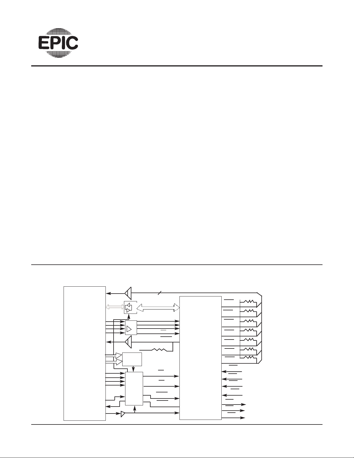
VMEbus /VERSAbus INTERFACE BLOCK DIAGRAM
IRQ1•
-IRQ7•
DO0-DO7
AO1
AO2
AO3
WRITE•
DTACK•
AO4-
A23
AMO-
AMX
DSO•
AS•
IACK•
SYSRESET•
IACKIN•
IACKOUT•
SYSCLK
EI68C153
BIM
IRQ1
IRQ2
IRQ3
IRQ4
IRQ5
IRQ6
IRQ7
•
•
•
•
•
•
•
•
•
•
•
•
•
•
Device A
Device B
Device C
Device D
INT0
INT1
INT2
INT3
Device
Interrupt
requests
INTAE
INTAL0
INTAL1
To Slave device
for external
interrupt Ack-
knowledge
System Bus
VMEbus of VERSAbus
DTACK
Control
Logic
Address
DEcode
IACKIN
IACKOUT
CS
IACK
A1
A2
A3
R/W
D0-D7
Data Bus
7
+5.0V
-5.0V
20
 Loading...