

EON EN29LV800JT-90TI, EN29LV800JT-90T, EN29LV800JT-70TI, EN29LV800JT-70T, EN29LV800JB-90TI Datasheet
...
4800 Great America Parkway, Suite 202 Tel: 408-235-8680
Santa Clara, CA 95054 Fax: 408-235-8685
1
EN29LV800J
Rev 0.1 Release Date: 2002/01/30
da0.
FEATURES
•
3V, single power supply operation
- Minimizes system level power requirements
•
Manufactured on 0.28 µm process technology
•
High performance
- Access times as fast as 70 ns
•
Low power consumption (typical values at 5
MHz)
- 7 mA typical active read current
- 15 mA typical program/erase current
- 1 µA typical standby current (standard access
time to active mode)
•
Flexible Sector Architecture:
- One 16 Kbyte, two 8 Kbyte, one 32 Kbyte, and
fifteen 64 Kbyte sectors (byte mode)
- One 8 Kword, two 4 Kword, one 16 Kword
and fifteen 32 Kword sectors (word mode)
- Supports full chip erase
- Individual sector erase supported
- Sector protection:
Hardware locking of sectors to prevent
program or erase operations within individual
sectors
Additionally, temporary Sector Group
Unprotect allows code changes in previously
locked sectors.
•
High performance program/erase speed
- Byte/Word program time: 8µs typical
- Sector erase time: 500ms typical
•
JEDEC Standard program and erase
commands
•
JEDEC standard
DATA
polling and toggle
bits feature
•
Single Sector and Chip Erase
•
Sector Unprotect Mode
•
Embedded Erase and Program Algorithms
•
Erase Suspend / Resume modes:
Read or program another Sector during
Erase Suspend Mode
•
0.28 µm double-metal double-poly
triple-well CMOS Flash Technology
•
Low Vcc write inhibit < 2.5V
• >100K program/erase endurance cycle
•
48-pin TSOP (Type 1)
•
Commercial Temperature Range
GENERAL DESCRIPTION
The EN29LV800J is an 8-Megabit, electrically erasable, read/write non-volatile flash memory,
organized as 1,048,576 bytes or 524,288 words. Any byte can be programmed typically in 10µs.
The EN29LV800JJ features 3.0V voltage read and write oper ation, with acces s times as fast as 70ns
to eliminate the need for WAIT states in high-performance microprocessor systems.
The EN29LV800J has separate Output Enable (
OE
), Chip Enable (CE), and Write Enable (WE)
controls, which eliminate bus contention issues. This device is designed to allow either single Sector
or full chip erase operation, where each Sector can be individually protected against program/erase
operations or temporarily unprotected to erase or program. The device can sustain a minimum of
100K program/erase cycles on each Sector.
EN29LV800J ******PRELIMINARY DRAFT******
8 Megabit (1024K x 8-bit / 512K x 16-bit) Flash Memory
Boot Sector Flash Memory, CMOS 3.0 Volt-only
4800 Great America Parkway, Suite 202 Tel: 408-235-8680
Santa Clara, CA 95054 Fax: 408-235-8685
2
EN29LV800J
Rev 0.1 Release Date: 2002/01/30
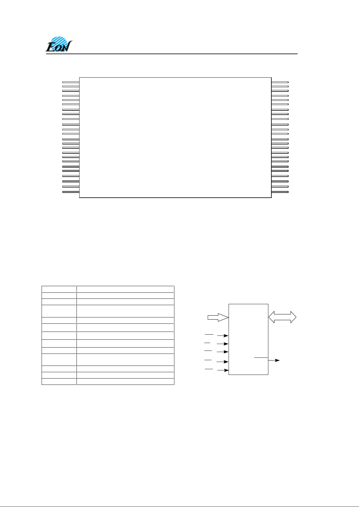
CONNECTION DIAGRAMS
TABLE 1. PIN DESCRIPTION FIGURE 1. LOGIC DIAGRAM
Pin Name Function
A0-A18 Addresses
DQ0-DQ14 15 Data Inputs/Outputs
DQ15 / A-1
DQ15 (data input/output, word mode),
A-1 (LSB address input, byte mode)
CE# Chip Enable
OE# Output Enable
RESET#
Hardware Reset Pin
RY/BY# Ready/Busy Output
WE# Write Enable
Vcc
Supply Voltage
(2.7-3.6V)
Vss Ground
NC Not Connected to anything
BYTE# Byte/Word Mode
EN29LV800J
DQ0 – DQ15
(A-1)
A0 - A18
WE
CE
OE
RY/BY
Reset
Byte
1
2
3
4
5
6
7
8
9
10
11
12
13
14
15
16
17
18
19
20
21
22
23
24
48
47
46
45
44
43
42
41
40
39
38
37
36
35
34
33
32
31
30
29
28
27
26
25
Standard
TSOP
A15
A14
A13
A12
A11
A10
A9
A8
NC
NC
WE#
RESET#
NC
NC
RY/BY#
A18
A17
A7
A6
A5
A4
A3
A2
A1
A16
BYTE#
Vss
DQ15/A-1
DQ7
DQ14
DQ6
DQ13
DQ5
DQ12
DQ4
Vcc
DQ11
DQ3
DQ10
DQ2
DQ9
DQ1
DQ8
DQ0
OE#
Vss
CE#
A0

4800 Great America Parkway, Suite 202 Tel: 408-235-8680
Santa Clara, CA 95054 Fax: 408-235-8685
3
EN29LV800J
Rev 0.1 Release Date: 2002/01/30
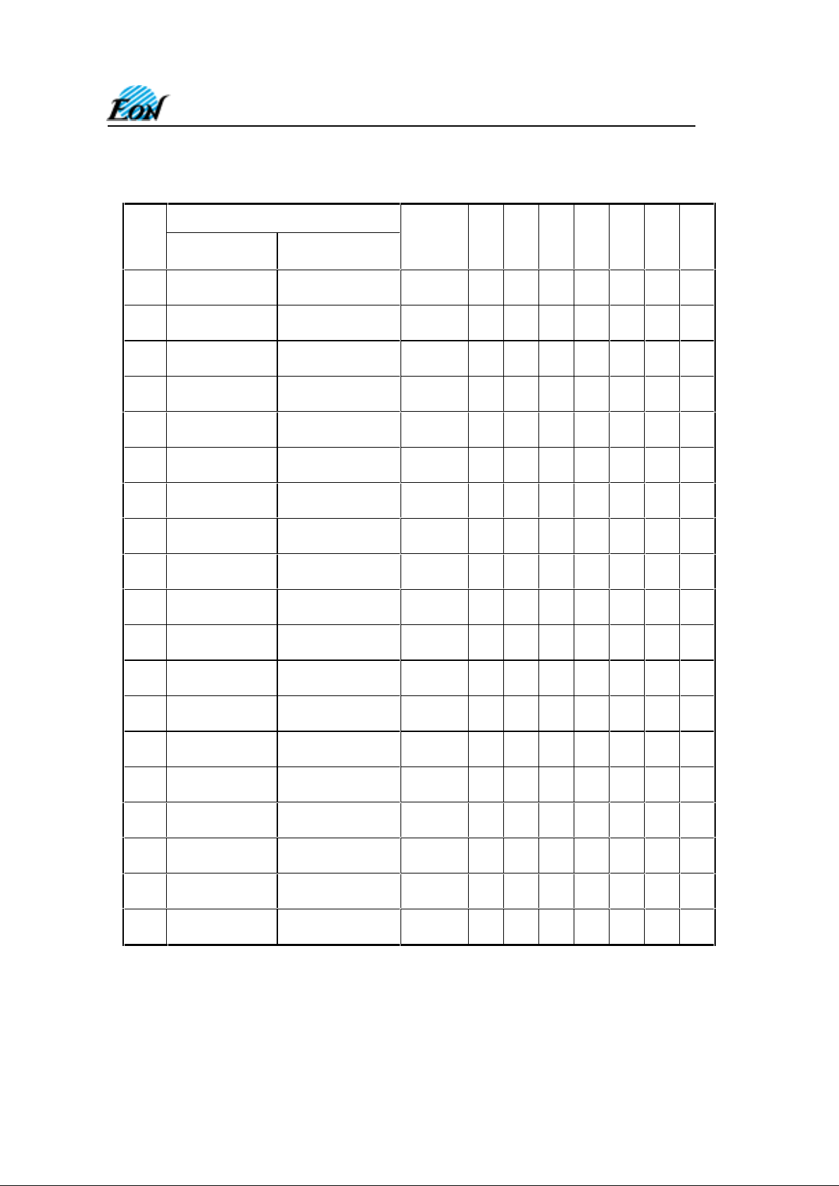
TABLE 2A. TOP BOOT BLOCK SECTOR ARCHITECTURE
ADDRESS RANGE
Sect
or
(X16) (X8)
SECTOR
SIZE
(Kbytes /
Kwords)
A18 A17 A16 A15 A14 A13 A12
18 7E000h-7FFFFh FC000h-FFFFFh 16/8 1 1 1 1 1 1 X
17 7D000h-7DFFFh FA000h-FBFFFh 8/4 1 1 1 1 1 0 1
16 7C000h-7CFFFh F8000h-F9FFFh 8/4 1 1 1 1 1 0 0
15 78000h-7BFFFh F0000h – F7FFFh 32/16 1 1 1 1 0 X X
14 70000h-77FFFh E0000h - EFFFFh 64/32 1 1 1 0 X X X
13 68000h-6FFFFh D0000h - DFFFFh 64/32 1 1 0 1 X X X
12 60000h-6FFFFh C0000h - CFFFFh 64/32 1 1 0 0 X X X
11 58000h-5FFFFh B0000h - BFFFFh 64/32 1 0 1 1 X X X
10 50000h-57FFFh A0000h - AFFFFh 64/32 1 0 1 0 X X X
9 48000h-4FFFFh 90000h - 9FFFFh 64/32 1 0 0 1 X X X
8 40000h-47FFFh 80000h - 8FFFFh 64/32 1 0 0 0 X X X
7 38000h-3FFFFh 70000h - 7FFFFh 64/32 0 1 1 1 X X X
6 30000h-37FFFh 60000h - 6FFFFh 64/32 0 1 1 0 X X X
5 28000h-2FFFFh 50000h – 5FFFFh 64/32 0 1 0 1 X X X
4 20000h-27FFFh 40000h – 4FFFFh 64/32 0 1 0 0 X X X
3 18000h-1FFFFh 30000h – 3FFFFh 64/32 0 0 1 1 X X X
2 10000h-17FFFh 20000h - 2FFFFh 64/32 0 0 1 0 X X X
1 08000h-0FFFFh 10000h - 1FFFFh 64/32 0 0 0 1 X X X
0 00000h-07FFFh 00000h - 0FFFFh 64/32 0 0 0 0 X X X
4800 Great America Parkway, Suite 202 Tel: 408-235-8680
Santa Clara, CA 95054 Fax: 408-235-8685
4
EN29LV800J
Rev 0.1 Release Date: 2002/01/30
TABLE 2B. BOTTOM BOOT BLOCK SECTOR ARCHITECTURE
ADDRESS RANGE
Sect
or
(X16) (X8)
SECTOR
SIZE
(Kbytes/
Kwords)
A18 A17 A16 A15 A14 A13 A12
18 78000h-7FFFFh F0000h – FFFFFh 64/32 1 1 1 1 X X X
17 70000h-77FFFh E0000h – EFFFFh 64/32 1 1 1 0 X X X
16 68000h-6FFFFh D0000h – DFFFFh 64/32 1 1 0 1 X X X
15 60000h-67FFFh C0000h – CFFFFh 64/32 1 1 0 0 X X X
14 58000h-5FFFFh B0000h - BFFFFh 64/32 1 0 1 1 X X X
13 50000h-57FFFh A0000h - AFFFFh 64/32 1 0 1 0 X X X
12 48000h-4FFFFh 90000h – 9FFFFh 64/32 1 0 0 1 X X X
11 40000h-47FFFh 80000h – 8FFFFh 64/32 1 0 0 0 X X X
10 38000h-3FFFFh 70000h –7FFFFh 64/32 0 1 1 1 X X X
9 30000h-37FFFh 60000h – 6FFFFh 64/32 0 1 1 0 X X X
8 28000h-2FFFFh 50000h – 5FFFFh 64/32 0 1 0 1 X X X
7 20000h-27FFFh 40000h – 4FFFFh 64/32 0 1 0 0 X X X
6 18000h-1FFFFh 30000h – 3FFFFh 64/32 0 0 1 1 X X X
5 10000h-17FFFh 20000h – 2FFFFh 64/32 0 0 1 0 X X X
4 08000h-0FFFFh 10000h – 1FFFFh 64/32 0 0 0 1 X X X
3 04000h-07FFFh 08000h – 0FFFFh 32/16 0 0 0 0 1 X X
2 03000h-03FFFh 06000h – 07FFFh 8/4 0 0 0 0 0 1 1
1 02000h-02FFFh 04000h – 05FFFh 8/4 0 0 0 0 0 1 0
0 00000h-01FFFh 00000h – 01FFFh 16/8 0 0 0 0 0 0 X
4800 Great America Parkway, Suite 202 Tel: 408-235-8680
Santa Clara, CA 95054 Fax: 408-235-8685
5
EN29LV800J
Rev 0.1 Release Date: 2002/01/30
PRODUCT SELECTOR GUIDE
Product Number EN29LV800J
Regulated Voltage Range: 3.0-3.6V
-70 -
Speed Option
Standard Voltage Range: Vcc=2.7 – 3.6V
- -90
Max Access Time, ns (t
acc
) 70 90
Max CE# Access, ns (tce) 70 90
Max OE# Access, ns (toe) 30 35
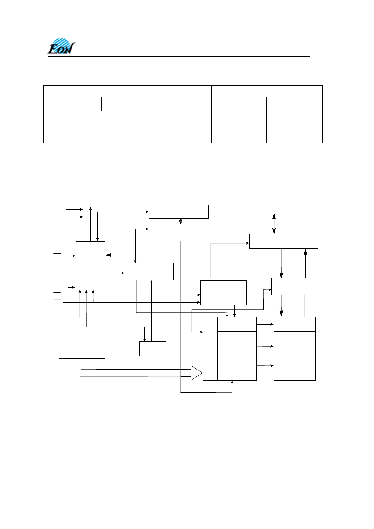
BLOCK DIAGRAM
WE
CE
OE
State
Control
Command
Register
Erase Voltage Generator
Input/Output Buffers
Program Voltage
Generator
Chip Enable
Output Enable
Logic
Data Latch
Y-Decoder
X-Decoder
Y-Gating
Cell Matrix
Timer Vcc Detector
A0-A18
Vcc
Vss
DQ0-DQ15 (A-1)
Address Latch
Block Protect Switches
STB
STB
RY/BY
4800 Great America Parkway, Suite 202 Tel: 408-235-8680
Santa Clara, CA 95054 Fax: 408-235-8685
6
EN29LV800J
Rev 0.1 Release Date: 2002/01/30
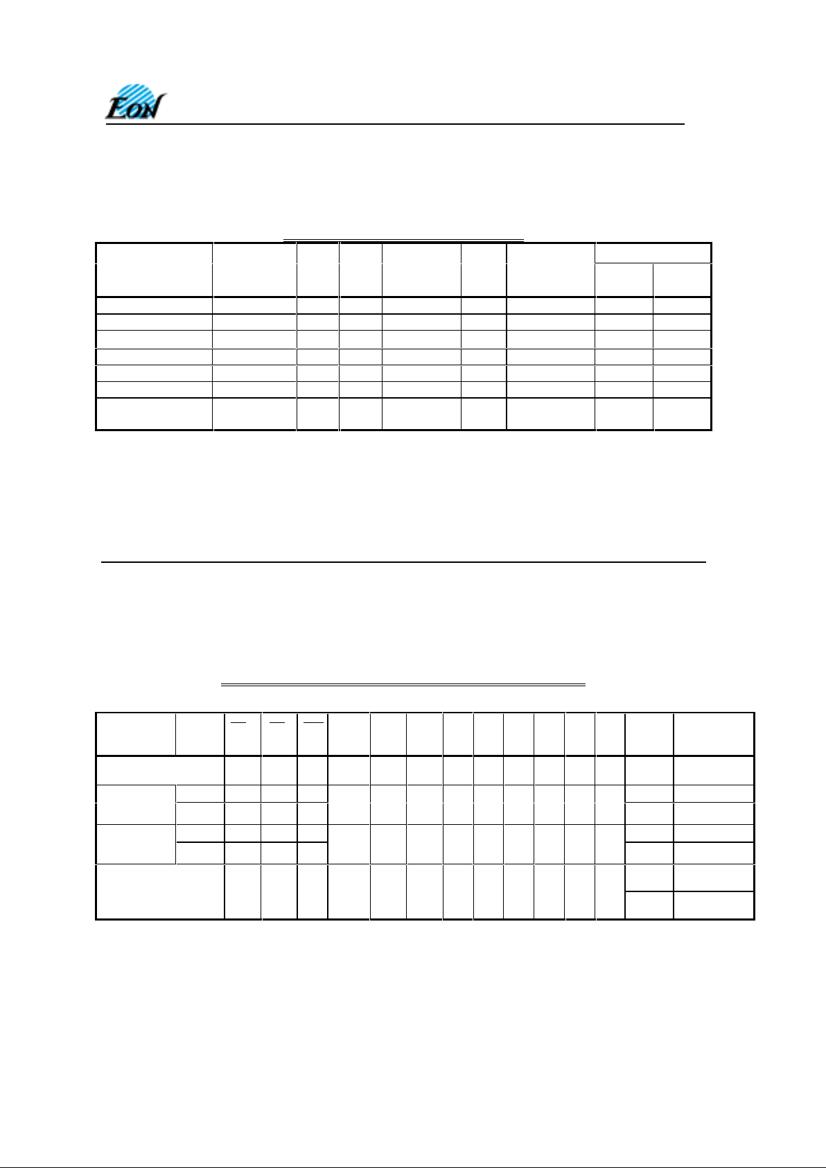
TABLE 3. OPERATING MODES
8M FLASH USER MODE TABLE
DQ8-DQ15
Operation CE# OE#
WE
# Reset#
A0A18 DQ0-DQ7
Byte#
= V
IH
Byte#
= VIL
Read L L H H AIN D
OUT
D
OUT
High-Z
Write L H L H AIN DIN D
IN
High-Z
CMOS Standby
V
cc
± 0.3V
X X
Vcc ± 0.3V
X High-Z High-Z High-Z
TTL Standby H X X H X High-Z High-Z High-Z
Output Disable L H H H X High-Z High-Z High-Z
Hardware Reset X X X L X High-Z High-Z High-Z
Temporary
Sector Unprotect X X X V
ID
A
IN
DIN D
IN
X
Notes:
L=logic low= V
IL
, H=Logic High= VIH, VID =11 ± 0.5V, X=Don’t Care (either L or H, but not f l oat i ng!),
D
IN
=Data In, D
OUT
=Data Out, AIN=Address In
TABLE 4. DEVICE IDENTIFICTION (Autoselect Codes)
8M FLASH MANUFACTURER/DEVICE ID TABLE
Note:
1. If a manufacturing ID is read with A 8=L, the chip will output a configuration code 7Fh. A further Manufacturing ID must be
read with A8=H.
2. A9 = VID is for HV A9 Autoselect mode onl y. A9 must be ≤ Vcc (CMOS l ogic level) for Command A utoselect Mode.
Description Mode A18
to
A12
A11
to
A10
A9
2
A8 A7 A6 A5
to
A2
A1 A0 DQ8
to
DQ15
DQ7 to
DQ0
Manufacturer ID:
Eon
L L H X X VID H1 X L X L L X 04h
Word L L H 22h DAh
Device ID
(top boot
block)
Byte L L H
X X VID X X L X L H
X DAh
Word L L H 22h 5Bh
Device ID
(bottom boot
block)
Byte L L H
X X VID X X L X L H
X 5Bh
X
01h
(Protected)
Sector Protection
Verification
L L H SA X VID X X L X H L
X
00h
(Unprotected)
OE
CE
WE

4800 Great America Parkway, Suite 202 Tel: 408-235-8680
Santa Clara, CA 95054 Fax: 408-235-8685
7
EN29LV800J
Rev 0.1 Release Date: 2002/01/30
USER MODE DEFINITIONS
Word / Byte Configuration
The signal set on the BYTE# Pin controls whether the device data I/O pins DQ15-DQ0 operate in the
byte or word configuration. When the Byte# Pin is set at logic ‘1’, then the device is in word
configuration, DQ15-DQ0 are active and are controlled by CE# and OE#.
On the other hand, if the Byte# Pin is set at logic ‘0’, then the device is in byte configuration, and only
data I/O pins DQ0-DQ7 are active and controlled by CE# and OE#. The data I/O pins DQ8-DQ14
are tri-stated, and the DQ15 pin is used as an input for the LSB (A-1) address function.
Standby Mode
The EN29LV800J has a CMOS-compatible standby mode, which reduces the
current to < 1µA
(typical). It is placed in CMOS-com patible standby when the
CE
pin is at VCC ± 0.5. RESET# and
BYTE# pin must also be at CMOS input levels. The device also has a TTL-compatible standby mode,
which reduces the maxim um V
CC
current to < 1mA. It is placed in TTL-c ompatible standby when the
CE
pin is at VIH. W hen in st andby modes, the outputs are in a high- im pedance state independent of
the
OE
input.
Read Mode
The device is automatically set to reading array data after device power-up. No commands are required to
retrieve data. The device is also ready to read array data after completing an Embedded Program or
Embedded Erase algorithm.
After the device accepts an Erase Suspend command, the device enters the Erase Suspend mode. The
system can read array data using the standard read timings, except that if it reads at an address within
erase-suspended sectors, the device outputs status data. After completing a programming operation in
the Erase Suspend mode, the system may once again read array data with the same exception. See
“Erase Suspend/Erase Resume Commands” for more additional information.
The system
must issue the reset command to re-enable the device for reading array data if DQ5 goes
high, or while in the autoselect mode. See the “Reset Command” additional details.
Output Disable Mode
When the
CE
or OE pin is at a logic high level (VIH), the output from the EN29LV800JJ is dis abled.
The output pins are placed in a high impedance state.
Auto Select Identification Mode
The autoselect mode provides manufacturer and device identification, and sector protection
verification, through identifier codes output on DQ15–DQ0. This mode is primarily intended for
programming equipment to automatically match a device to be programmed with its corresponding
programming algorithm. However, the autoselect codes can also be accessed in-system through the
command register.
When using programming equipment, the autoselect mode requires V
ID
(10.5 V to 11.5 V) on
address pin A9. Address pins A8, A6, A1, and A0 must be as shown in Autoselect Codes table. In
addition, when verifying sector protection, the sector address must appear on the appropriate highest
order address bits. Refer to the corresponding Sector Address Tables. The Command Definitions
table shows the remaining address bits that are don’t-care. When all necessary bits have been set as
required, the programming equipment may then read the corresponding identifier code on DQ15–
DQ0.
4800 Great America Parkway, Suite 202 Tel: 408-235-8680
Santa Clara, CA 95054 Fax: 408-235-8685
8
EN29LV800J
Rev 0.1 Release Date: 2002/01/30
To access the autoselect codes in-system; the host system can issue the autoselect command via
the command register, as shown in the Command Definitions table. This method does not require
V
ID
. See “Command Definitions” for details on using the autoselect mode.
Write Mode
Write operations, including programming data and erasing sectors of memory, require the host
system to write a command or command sequence to the device. Write cycles are initiated by
placing the byte or word address on the device’s address inputs while the data to be written is input
on DQ[7:0] in Byte Mode (BYTE# = L) or on DQ[15:0] in Word Mode (BYTE# = H). The host system
must drive the CE# and WE# pins Low and the OE# pin High for a valid write operation to take place.
All addresses are latched on the falling edge of WE# and CE#, whichever happens later. All data is
latched on the rising edge of WE# or CE#, whichever happens first. The system is not required to
provide further controls or timings. The device automatically provides internally generated program /
erase pulses and verifies the programmed /erased cells’ margin. The host system can detect
completion of a program or erase operation by observing the RY/BY# pin, or by reading the DQ[7]
(Data# Polling) and DQ[6] (Toggle) status bits.
The ‘Command Definitions’ section of this document provides details on the specific device
commands implemented in the EN29LV800J.
Sector Protection/Unprotection
The hardware sector protection feature disables both program and erase operations in any sector. The
hardware sector unprotection feature re-enables both program and erase operations in previously
protected sectors.
There are two methods to enabling this hardware pr otection circ uitry. The firs t one requires only that
the RESET# pin be at V
ID
and then standard microprocessor timings can be used to enable or
disable this feature. See Flowchart 7a and 7b for the algorithm and Figure 12 for the timings.
When doing Sector Unprotect, all the other sectors should be protected first.
The second method is meant for programming equipment. This method requires V
ID
be applied to
both OE# and A9 pin and non-standard microprocessor timings are used. This method is described
in a separate document called EN29LV800J Supplement,
which can be obtained by contacting a
representative of Eon Silicon Devices, Inc.
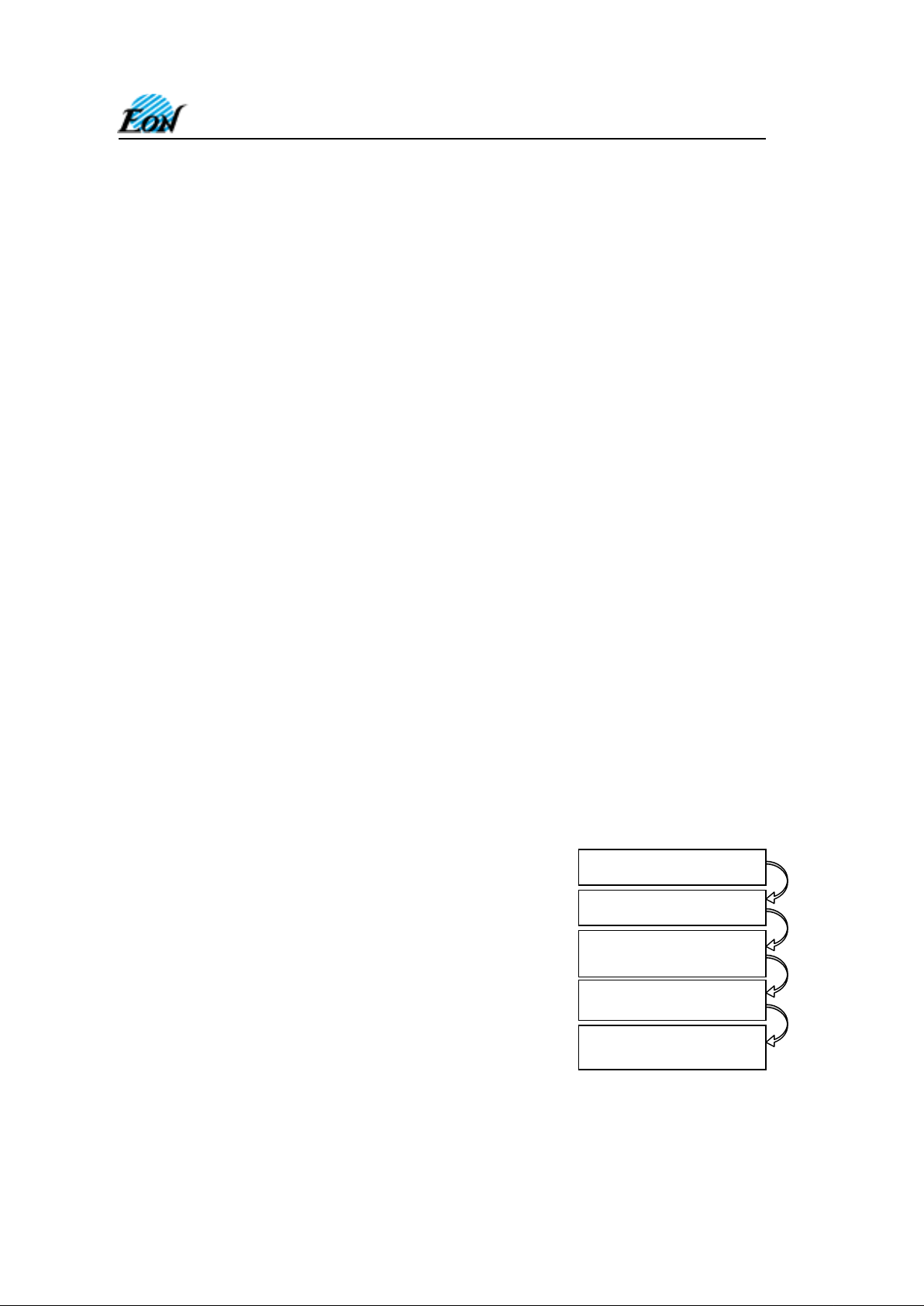
Temporary Sector Unprotect
This feature allows temporary unprotection of previously protected
sector groups to change data while in-system. The Sector
Unprotect mode is activated by setting the RESET# pin to V
ID
.
During this mode, formerly protected sectors can be programmed
or erased by simply selecting the sector addresses. Once is
removed from the RESET# pin, all the previously protected sectors
are protected again. See accompanying figure and timing
diagrams for more details.
Start
Reset#=VID (note 1)
Perform Erase or Program
Operations
Reset#=VIH
Temporary Sector
Unprotect Completed
(note 2)
Notes:
1. All protected sectors unprotected.
2. Previously protected sectors protected
again.

4800 Great America Parkway, Suite 202 Tel: 408-235-8680
Santa Clara, CA 95054 Fax: 408-235-8685
9
EN29LV800J
Rev 0.1 Release Date: 2002/01/30
Automatic Sleep Mode
The automatic sleep mode minimizes Flash device energy consumption. The device automatically
enables this mode when addresses remain stable for t
acc
+ 30ns. The automatic sleep mode is
independent of the CE#, WE# and OE# control signals. Standard address access timings provide
new data when addresses are changed. While in sleep mode, output is latched and always
available to the system. ICC
4
in the DC Characteristics table represents the automatic sleep more
current specification.

4800 Great America Parkway, Suite 202 Tel: 408-235-8680
Santa Clara, CA 95054 Fax: 408-235-8685
10
EN29LV800J
Rev 0.1 Release Date: 2002/01/30
Hardware Data Protection
The command sequence requirement of unlock cycles for programming or erasing provides data
protection against inadvertent writes as seen in the Command Definitions table. Additionally, the
following hardware data protection measures prevent accidental erasure or programming, which
might otherwise be caused by false system level signals during Vcc power up and power down
transitions, or from system noise.
Low VCC Write Inhibit
When Vcc is less than V
LKO
, the device does not accept any write cycles. This protects data during
Vcc power up and power down. The command register and all internal program/erase circuits are
disabled, and the device resets. Subsequent writes are ignored until Vcc is greater than V
LKO
. The
system must provide the proper signals to the control pins to prevent unintentional writes when Vcc is
greater than V
LKO
.
Write Pulse “Glitch” protection
Noise pulses of less than 5 ns (typical) on
OE
, CE or
WE
do not initiate a write cycle.
Logical Inhibit
Write cycles are inhibited by holding any one of
OE
= VIL, CE = VIH, or
WE
= VIH
. To initiate a
write cycle,
CE
and
WE
must be a logical zero while
OE
is a logical one. If CE,
WE
, and OE
are all logical zero (not recommended usage), it will be considered a read.
Power-up Write Inhibit
During power-up, the device automatically resets to READ mode and locks out write cycles. Even
with
CE
= VIL, WE = VIL and OE = VIH, the device will not accept commands on the rising edge of
WE
.

4800 Great America Parkway, Suite 202 Tel: 408-235-8680
Santa Clara, CA 95054 Fax: 408-235-8685
11
EN29LV800J
Rev 0.1 Release Date: 2002/01/30
COMMAND DEFINITIONS
The operations of the EN29LV800J are selected by one or more commands written into the
command register to perform Read/Reset Memory, Read ID, Read Sector Protection, Program,
Sector Erase, Chip Erase, Erase Suspend and Er ase Resume. Comm ands are made up of data
sequences written at specific addresses via the command register. The sequences for the
specified operation are defined in the Command Definitions table (Table 5). Incorrect address es,
incorrect data values or improper sequences will reset the device to Read Mode.
Table 5. EN29LV800J Command Definitions
Bus Cycles
1
st
Write Cycle
2
nd
Write Cycle
3
rd
Write Cycle
4
th
Write Cycle
5
th
Write Cycle
6
th
Write Cycle
Command
Sequence
Cycles
Add Data Add Data Add Data Add Data Add Data Add Data
Read 1 RA RD
Reset 1 xxx F0
Word 555 2AA 555
000/
001
7F/
1C
Manufacturer
ID
Byte
4
AAA
AA
555
55
AAA
90
000/
001
7F/
1C
Word 555 2AA 555 X01 22DA Device ID
Top Boot
Byte
4
AAA
AA
555
55
AAA
90
X02 DA
Word 555 2AA 555 X01 225B Device ID
Bottom Boot
Byte
4
AAA
AA
555
55
AAA
90
X02 5B
XX00
Word 555
2AA
555
(SA)
X02
XX01
00
Autoselect
Sector Protect
Verify
Byte
4
AAA
AA
555
55
AAA
90
(SA)
X04
01
Word 555 2AA 555
Program
Byte
4
AAA
AA
555
55
AAA
A0 PA PD
Word 555 2AA 555
Unlock Bypass
Byte
3
AAA
AA
555
55
AAA
20
Unlock Bypass Program 2 XXX A0 PA PD
Unlock Bypass Res et 2 XXX 90 XXX 00
Word 555 2AA 555 555 2AA 555
Chip Erase
Byte
6
AAA
AA
555
55
AAA
80
AAA
AA
555
55
AAA
10
Word 555 2AA 555 555 2AA
Sector Erase
Byte
6
AAA
AA
555
55
AAA
80
AAA
AA
555
55 SA 30
Erase Suspend 1 xxx B0
Erase Resume 1 xxx 30
Address and Data values indicat ed i n hex
RA = Read Address: address of the memory location to be read. Thi s is a read cycle.
RD = Read Data: data read from locat i on RA duri ng Read operation. This is a read cycle.
PA = Program Address: address of the memory locat i on to be programmed. X = Don’t-Care
PD = Program Data: data to be programmed at location PA
SA = Sector Address: address of the Sector to be erased or verif i ed. Address bits A18-A12 uniquely select any Sector.
Reading Array Data
The device is automatically set to reading array data after power up. No commands are required to
retrieve data. The device is also ready to read array data after completing an Embedded Program or
Embedded Erase algorithm.
Following an Erase Suspend command, Erase Suspend mode is entered. The system can read array
data using the standard read timings, with the only difference in that if it reads at an address within erase
suspended sectors, the device outputs status data. After completing a programming operation in the
Erase Suspend mode, the system may once again read array data with the same exception.

4800 Great America Parkway, Suite 202 Tel: 408-235-8680
Santa Clara, CA 95054 Fax: 408-235-8685
12
EN29LV800J
Rev 0.1 Release Date: 2002/01/30
The Reset command must be issued to re-enable the device for reading array data if DQ5 goes high, or
while in the autoselect mode. See next section for details on Reset.
Reset Command
Writing the reset command to the device resets the device to reading array data. Address bits are don’tcare for this command.
The reset command may be written between the sequence cycles in an erase command sequence before
erasing begins. This resets the device to reading array data. Once erasure begins, however, the device
ignores reset commands until the operation is complete. The reset command may be written between the
sequence cycles in a program command sequence before programming begins. This resets the device to
reading array data (also applies to programming in Erase Suspend mode). Once programming begins,
however, the device ignores reset commands until the operation is complete.
The reset command may be written between the sequence cycles in an autoselect command sequence.
Once in the autoselect mode, the reset command
must be written to return to reading array data (also
applies to autoselect during Erase Suspend).
If DQ5 goes high during a program or erase operation, writing the reset command returns the device to
reading array data (also applies during Erase Suspend).
Autoselect Command Sequence
The autoselect command sequence allows the host system to access the manufacturer and devices
codes, and determine whether or not a sector is protected. The Command Definitions table shows the
address and data requirements. This is an alternative to the method that requires V
ID
on address bit A9
and is intended for PROM programmers.
Two unlock cycles followed by the autoselect command initiate the autoselect command sequence.
Autoselect mode is then entered and the system may read at addresses shown in Table 4 any number of
times, without needing another command sequence.
The system must write the reset command to exit the autoselect mode and return to reading array data.
Word / Byte Programming Command
The device may be programmed by byte or by word, depending on the state of the Byte# Pin.
Programming the EN29LV800J is performed by using a four bus-cycle operation (two unlock write
cycles followed by the Program Setup command and Program Data Write cycle). When the program
command is executed, no additional CPU controls or timings are necessary. An internal timer
terminates the program operation automatically. Address is latched on the falling edge of
CE
or
WE
, whichever is last; data is latched on the rising edge of CE or
WE
, whichever is first.
Programming status may be checked by sampling data on DQ7 (
DATA
polling) or on DQ6 (toggle
bit). ). When the program operation is successfully completed, the device returns to read mode and
the user can read the data programmed to the device at that address. Note that data can not be
programmed from a 0 to a 1. Only an erase operation can change a data from 0 to 1. When
programming time limit is exceeded, DQ5 will produce a logical “1” and a Reset command can return
the device to Read mode.
Unlock Bypass
To speed up programming operation, the Unlock Bypass Command may be used. Once this feature
is activated, the shorter two cycle Unlock Bypass Program command can be used instead of the
normal four cycle Program Command to program the device. This mode is exited after issuing the
Unlock Bypass Reset Command. The device powers up with this feature disabled.

4800 Great America Parkway, Suite 202 Tel: 408-235-8680
Santa Clara, CA 95054 Fax: 408-235-8685
13
EN29LV800J
Rev 0.1 Release Date: 2002/01/30
Chip Erase Command
Chip erase is a six-bus-cycle operation. The chip erase command sequence is initiated by writing two
unlock cycles, followed by a set-up command. Two additional unlock write cycles are then followed by the
chip erase command, which in turn invokes the Embedded Erase algorithm. The device does
not require
the system to preprogram prior to erase. The Embedded Erase algorithm automatically preprograms and
verifies the entire memory for an all zero data pattern prior to electrical erase. The system is not required
to provide any controls or timings during these operations. The Command Definitions table shows the
address and data requirements for the chip erase command sequence.
Any commands written to the chip during the Embedded Chip Erase algorithm are ignored.
The system can determine the status of the erase operation by using DQ7, DQ6, or DQ2. See “Write
Operation Status” for information on these status bits. When the Embedded Erase algorithm is complete,
the device returns to reading array data and addresses are no longer latched.
Flowchart 4 illustrates the algorithm for the erase operation. See the Erase/Program Operations tables in
“AC Characteristics” for parameters, and to the Chip/Sector Erase Operation Timings for timing
waveforms.
Sector Erase Command Sequence
Sector erase is a six bus cycle operation. The sector erase command sequence is initiated by writing two
un-lock cycles, followed by a set-up command. Two additional unlock write cycles are then followed by
the address of the sector to be erased, and the sector erase command. The Command Definitions table
shows the address and data requirements for the sector erase command sequence.
Once the sector erase operation has begun, only the Erase Suspend command is valid. All other
commands are ignored.
When the Embedded Erase algorithm is complete, the device returns to reading array data and addresses
are no longer latched. The system can determine the status of the erase operation by using DQ7, DQ6, or
DQ2. Refer to “Write Operation Status” for information on these status bits. Flowchart 4 illustrates the
algorithm for the erase operation. Refer to the Erase/Program Operations tables in the “AC
Characteristics” section for parameters, and to the Sector Erase Operations Timing diagram for timing
waveforms.
Erase Suspend / Resume Command
The Erase Suspend command allows the system to interrupt a sector erase operation and then read data
from, or program data to, any sector not selected for erasure. This command is valid only during the
sector erase operation. The Erase Suspend command is ignored if written during the chip erase operation
or Embedded Program algorithm. Addresses are don’t-cares when writing the Erase Suspend command.
When the Erase Suspend command is written during a sector erase operation, the device requires a
maximum of 20 µs to suspend the erase operation.
After the erase operation has been suspended, the system can read array data from or program data to
any sector not selected for erasure. (The device “erase suspends” all sectors selected for erasure.)
Normal read and write timings and command definitions apply. Reading at any address within erasesuspended sectors produces status data on DQ7–DQ0. The system can use DQ7, or DQ6 and DQ2
together, to determine if a sector is actively erasing or is erase-suspended. See “Write Operation Status”
for information on these status bits.
After an erase-suspended program operation is complete, the system can once again read array data
within non-suspended sectors. The system can determine the status of the program operation using the
DQ7 or DQ6 status bits, just as in the standard program operation. See “Write Operation Status” for more
information. The Autoselect command is not supported during Erase Suspend Mode.
 Loading...