

Page 1

Inside SQ80 – a technical description
Rainer Buchty
eMail: rainer@buchty.net
http://www.buchty.net
September 29, 1999
Page 2

Page 3

Abstract
Since Ensoniq refuses to give any technical information about the SQ80
Cross Wave Synthesizer someone had to do the job... I hope this documentation will help the electronically skilled to repair and/or improve their
beloved machine. At least it will give some deeper understanding of what’s
going on inside.
Page 4

Contents
1 Introduction 5
1.1 What is the (E)SQ family of synthesizers all about? . . . . . 6
1.2 Synthesis Parameters . . . . . . . . . . . . . . . . . . . . . . . 6
1.3 The sequencer . . . . . . . . . . . . . . . . . . . . . . . . . . . 8
1.4 Multitimbrality - I need more voices! . . . . . . . . . . . . . . 8
2 Technical Documentation 11
2.1 System Overview . . . . . . . . . . . . . . . . . . . . . . . . . 12
2.2 The one which drives it all: MC6809E . . . . . . . . . . . . . 13
2.3 Let there be sound: DOC5503 and CEM3379 . . . . . . . . . 14
2.4 The art of disk storage . . . . . . . . . . . . . . . . . . . . . . 15
2.4.1 Track Layout . . . . . . . . . . . . . . . . . . . . . . . 15
2.4.2 Disk Directory Structure . . . . . . . . . . . . . . . . . 16
2.4.3 Sequencer Memory Dumps . . . . . . . . . . . . . . . 16
2.4.4 Bank Files . . . . . . . . . . . . . . . . . . . . . . . . 17
2.4.5 Program Files . . . . . . . . . . . . . . . . . . . . . . . 17
2.5 What comes in, must come out - the I/O subsystem . . . . . 19
2.6 The system software . . . . . . . . . . . . . . . . . . . . . . . 20
2.6.1 OSRAM . . . . . . . . . . . . . . . . . . . . . . . . . . 20
2.6.2 Cartridge . . . . . . . . . . . . . . . . . . . . . . . . . 20
2.6.3 Hidden Functions . . . . . . . . . . . . . . . . . . . . . 20
3 Troubleshooting 23
3.1 General problems . . . . . . . . . . . . . . . . . . . . . . . . . 24
3.2 MIDI mysteries . . . . . . . . . . . . . . . . . . . . . . . . . . 25
3.3 Keyboard Trouble . . . . . . . . . . . . . . . . . . . . . . . . 25
3.4 Storage Hassles . . . . . . . . . . . . . . . . . . . . . . . . . . 26
3.5 Panel Problems . . . . . . . . . . . . . . . . . . . . . . . . . . 26
3.6 Flaky Tape . . . . . . . . . . . . . . . . . . . . . . . . . . . . 26
A Parts List 27
B Schematics 29
2
Page 5

CONTENTS 3
C Datasheets 39
C.1 WD1770/1772 Floppy Disk Controller / Formatter . . . . . . 41
C.1.1 Description . . . . . . . . . . . . . . . . . . . . . . . . 41
C.1.2 Architecture . . . . . . . . . . . . . . . . . . . . . . . 41
C.1.3 Processor Interface . . . . . . . . . . . . . . . . . . . . 43
C.1.4 General Disk Read Operation . . . . . . . . . . . . . . 45
C.1.5 General Disk Write Operation . . . . . . . . . . . . . 45
C.1.6 Command Description . . . . . . . . . . . . . . . . . . 46
C.1.7 Type 1 Commands . . . . . . . . . . . . . . . . . . . . 48
C.1.8 Type 2 Commands . . . . . . . . . . . . . . . . . . . . 50
C.1.9 Type 3 Commands . . . . . . . . . . . . . . . . . . . . 52
C.1.10 Type 4 Commands . . . . . . . . . . . . . . . . . . . . 54
C.1.11 Status Register . . . . . . . . . . . . . . . . . . . . . . 55
C.1.12 Recommended Layout for 128-Byte Sectors . . . . . . 56
C.1.13 Recommended Layout for 256-Byte Sectors . . . . . . 57
C.1.14 Generic (non-standard) formats . . . . . . . . . . . . . 58
C.2 SSM2300 Octal Sample&Hold . . . . . . . . . . . . . . . . . . 61
C.3 MC/SN 2681 DUART . . . . . . . . . . . . . . . . . . . . . . 63
C.4 CEM3360 Dual VCA . . . . . . . . . . . . . . . . . . . . . . . 89
C.5 CEM3379 Analog Signal Processor . . . . . . . . . . . . . . . 93
C.6 Ensoniq DOC5503 . . . . . . . . . . . . . . . . . . . . . . . . 103
C.6.1 Common Registers . . . . . . . . . . . . . . . . . . . . 103
C.6.2 DOC registers for individual Oscillators . . . . . . . . 103
C.6.3 Wavetable Address Generation . . . . . . . . . . . . . 106
C.6.4 Pinout . . . . . . . . . . . . . . . . . . . . . . . . . . . 107
C.7 MC/HD 68B09E CPU . . . . . . . . . . . . . . . . . . . . . . 109
C.8 AD7524 Analog/Digital Converter . . . . . . . . . . . . . . . 145
Page 6

4 CONTENTS
Page 7

Chapter 1
Introduction
The SQ80 was released at the beginning of 1988 (at least here Europe) and
was one of the first so-called workstations. It not only was a synthesizer
but also came along with a 8-track sequencer. Obviously, it also featured
multi-timbrality and dynamic voice allocation which was quite a novum.
And as one of the first synthesizers it was equipped with a 3.5” disk drive
- no need for expensive sound cartridges or excessive bulk dump sessions
anymore.
What also made the (E)SQ family of synthesizers a success was the
easy-to-use user interface. Unlike most synthesizers of that time where
one had to select a parameter by number (!) and editing that one again
by number (sometimes even in hexadecimal) the SQ80 came (as its little
brother the ESQ-1) with a big alpha-numeric display and a load of buttons
each being responsible for a group of functions.
Unfortunately, the early Ensoniq synths and accessories for these such
as the single output expansion unit disappeared completely after the first
TransWave
T M
synthesizer – the VFX – hit the market.
5
Page 8
6 CHAPTER 1. INTRODUCTION
OSC #1
OSC #2
OSC #3
DCA #1
DCA #2
DCA #3
VCF VCA/PAN
LFO #2LFO #1 LFO #3
EG #1 EG #2 EG #3 EG #4
Sync
AM
1.1 What is the (E)SQ family of synthesizers all
about?
The (E)SQ synthesizers aswell as Ensoniq’s first sampler (which was a great
success) are based on the so called DOC chip. This abbreviation stands for
Digital Oscillator Circuit and is the musical heart of all of these machines.
Speaking of the synthesizers we could say that the SQ80 is a superset of the
ESQ-1 offering the following enhancements:
• bigger waveform memory (75 waves including the 32 ESQ-1 waves)
• bigger sequencer memory (64kB by default)
• built-in 3.5” disk drive
• keyboard with polyphonic aftertouch
What makes the (E)SQ synthesizers (even today!) quite interesting is
their great flexibility. They can either sound warm and analog but also cold
and digital. The reason lies in their hybrid nature – digital oscillators but
analog sound processing. The factory presets give a rough overview over the
SQ80’s capabilies but to get a real impression of what this machine can do
should get e.g. the Transoniq Hacker patches.
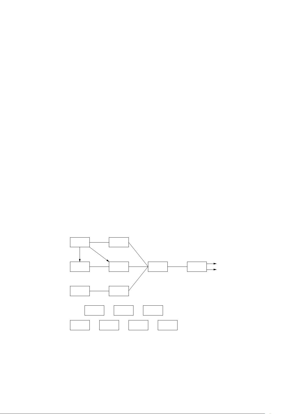
1.2 Synthesis Parameters
Figure 1.1 shows the basic architecture of each voice:
Figure 1.1: Architecture of an SQ80 voice
Page 9

1.2. SYNTHESIS PARAMETERS 7
Unlike modern synthesizers where a single voice mostly consists of an
oscillator plus filters the SQ80 offers 3 oscillators per voice (using 4 oscillators
might have overextended the CPU’s capabilities, I just don’t know) which
gives it a rich base sound. Also pretty nice is that per voice four envelope
generators and three LFOs exist – soundprogrammer’s heaven. Besides, the
SQ80 offers some more features which I will explain as follows:
Gated Mode: Besides some one-shot (not loopable) waveforms the SQ80
offers a special playback mode where an Envelope is only processed
once treating the sustain level as just an ordinary envelope step. This
is nice for producing percussive sounds which don’t need a sustain
phase.
Synchronization: You know that fancy “EEEOOOOW” sounds? It’s the
audible effect of one oscillator synchronizing another. The SQ80 can
produce these, too, since the DOC chip supports oscillator synchronization - unfortunately only between an even/odd pair of oscillators,
that’s why only synchronizing OSC2 by OSC1 is possible.
Amplitude Modulation: Good for making gong sounds or any other
which need disharmonic spectrals. Not quite the same as ring modulation but pretty close.
Oscillator Restart In usual DCO-based synthesizers the oscillator starts
playing back a wave from its very beginning when a key is played.
This is ok for complex waves but results in a static sound when using
short, looped waves such as e.g. SAW. Thinking of analog oscillators
such a reset of the waveform is unnatural (saw oscillators are based
on integrators) - the SQ80 offers both: oscillator reset or free-running
waves. However, this can be only programmed per sound program,
not individual for each oscillator.
LFO Specialties: Instead of a fixed output amplitude the modula-
tion depth of each LFO can be programmed to fade in (or out).
If that’s not enough an assignable modulation depth modulator exists.
Digitally controlled synthesizers tend to offer very static LFOs: As
soon as you hit a key the LFO starts at position 0 of the selected wave
- this is very annoying when using the LFO for e.g. filter sweeps, so
the SQ80’s LFOs can be programmed to be running freely or being
reset by each keystroke. And if you think that digital LFOs sound too
static – switch on the HUMANIZE function!
Envelope Specialties: Not much uncommon here, but for completeness’
sake I’d mention that an envelope generator can be programmed
Page 10

8 CHAPTER 1. INTRODUCTION
to react on key velocity (linear and exponential response) and key
position. What’s really fancy about the envelopes is that the so called
second release which does not really replace a reverb but produces a
similar effect.
Of course the envelopes are not of ADSR-type but a 4 level/rate model.
1.3 The sequencer
Normally, on-board sequencers are a nice add-on but nothing more. Not
the SQ80 built-in sequencer which is really useful. It’s a pattern-oriented
sequencer capable of holding up to 20 songs consisting of up to 60 sequences. What makes it so useful is the fact that you not only have a basic
record/quantize/playback functionality but also the capabilites of track
transpose, sequence editing (add/delete bars) and even single step editing
of track contents. Also it contains a very flexible song editor and locator.
Needless to say that the sequencer not only can be controlled by MIDI but
also synchronized to MIDI clock or Tape Sync.
On the “minus” side there’s only few. Have you ever tried to attach a
new volume level to an existing track after having recorded it? On earlier
software versions this is impossible.
1.4 Multitimbrality - I need more voices!
The SQ80 was one of the first synthesizers offering multitimbrality which
means that one machine was able to play independent sounds on each voice
(to that time we used the term MIDI multi mode capable which is pretty
the same).
Unfortunately, the SQ80 offers only 8 voices which is not much if you
think of complex arrangements. Fortunately, it has a really neat voice
allocation algorithm (much better as the very static one used e.g. in the
Yamaha SY-77) which can be influenced per sound program individually.
Think of natural instruments - if you play the same note twice the
previously played note will be replaced by the following one. The SQ80
can mimic this behaviour – or disregard nature, just as you like. But keep
in mind that the latter one forces a more aggressive voice allocation since
there’s no oscillator to “recycle”.
Lucky people (such as me :-) own more than one SQ80 – and can easily
daisy-chain these by enabling the overflow mode. This means that any note
Page 11

1.4. MULTITIMBRALITY - I NEED MORE VOICES! 9
which an SQ80 can’t play since all oscillators are used will be handed down
the chain to another SQ80 which might have free resources.
Page 12

10 CHAPTER 1. INTRODUCTION
Page 13

Chapter 2
Technical Documentation
I’ve asked Ensoniq three times for the original technical documentation of
the SQ80, here’s what they responded:
1. “The schematics are proprietary and not meant to be given away.”
(This was after my naive(?) first-time asking, but hey, I got the
schematics of my Yamaha equipment aswell - and these are far more
high-tech!)
2. “Your work sounds incredible – but we wish you all the best.” (after
telling them that I started to reverse-engineer the SQ80)
3. “Congratulations on your work!” (when finally telling them that I
succeeded in drawing schematics, documenting the OS and creating
an assembly language source code for further OS development)
With no word they told me that they dislike these efforts, neither they
told me to keep that knowledge for myself. So here it comes...
11
Page 14
12 CHAPTER 2. TECHNICAL DOCUMENTATION
Sequencer Memory
DOS Memory
Operating System
System Memory
CPU
DUART
Cart. MIDI
Keybrd.
&
Displ.
Control
Address Decodier
Floppy
Drive
DOC
FDC
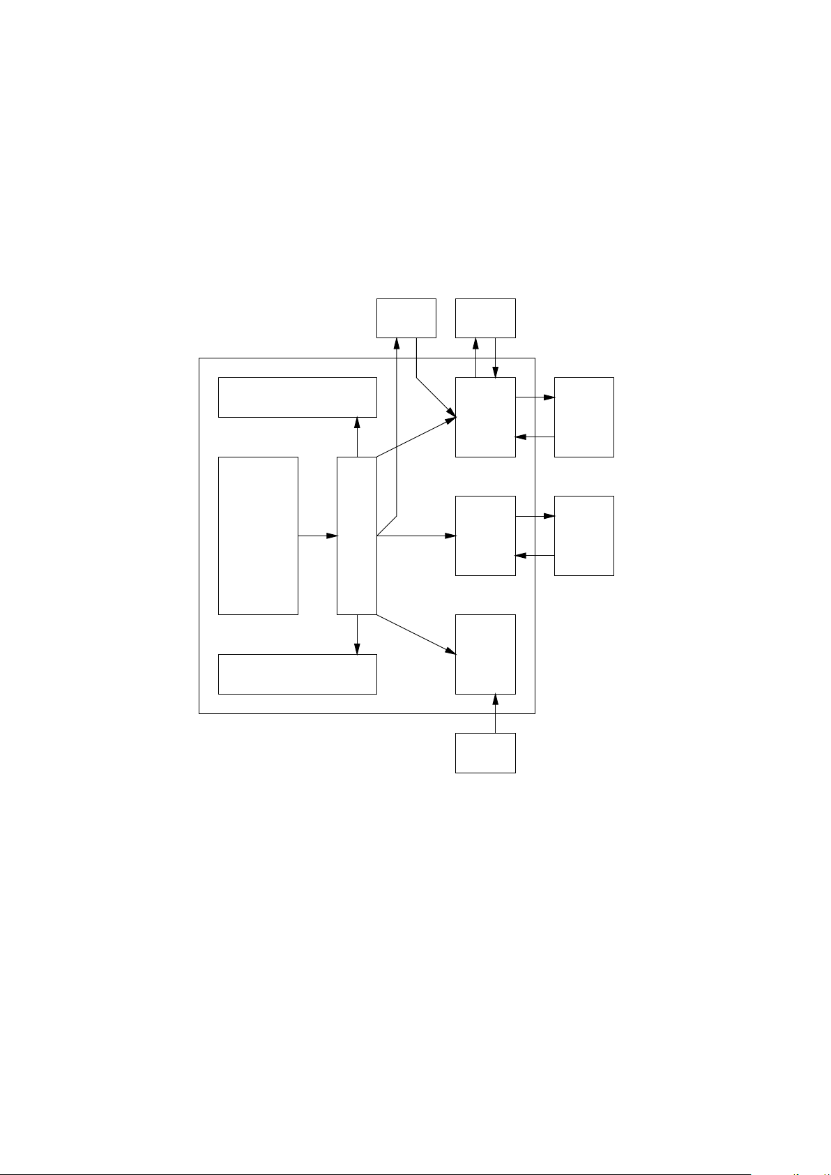
2.1 System Overview
Basically, the SQ80 is nothing more than a microcomputer with some specialized peripherals. Figure 2.1 gives an overview over the system architecture:
Figure 2.1: Anatomy of an SQ80
Mostly computer stuff, the only dedicated “musical” parts are the DOC
and the analog sound processors. This is a big advantage over other, especially modern synthesizers, since you can get replacement parts from the
next distributor of electronic parts.
Page 15

2.2. THE ONE WHICH DRIVES IT ALL: MC6809E 13
2.2 The one which drives it all: MC6809E
The Motorola 6809 was widely used for synthesizers back in the 80’s.
Not only Ensoniq did use it in their (E)SQ synthesizers and the Mirage
samplers, it’s also the heart of e.g. the Oberheim XPander. And even the
DX-7 used some special kind of 6809, the Hitachi 6309 (an improved 6809).
What made the 6809 that attractive was its computing power combined
with a very flexible instruction set. The SQ80 makes heavy use of the 6809’s
specialties:
• loadable system stack pointer S (used for context switching)
• loadable user stack pointer U (used as another 16-bit index register)
• 16-bit index registers X and Y
• 16-bit accumulator D
• fast (integer) multiplication / division
• software interrupts (used for error signalling)
• SYNC and CWAI commands forcing the CPU to wait for an external
interrupt
In the SQ80 the 6809E was used. Unlike the 6809 it’s E–mate could be
completely externally controlled which is needed inside the SQ80 where the
generation of clock signals is influenced by the DOC chip. See p.111 for
details on this processor.
Page 16

14 CHAPTER 2. TECHNICAL DOCUMENTATION
2.3 Let there be sound: DOC5503 and CEM3379
Some of you might know that the creator of the DOC, Bob Yannes, was
also the designer of the all famous SID chip which was the sound engine of
the Commodore 64 home computer. Both are based on the same principle:
phase accumulation. This means that the frequency of a digital voice is
not determined by the playback frequency (clock) as it was used in former
drum computers (and which will drive every today’s studio technician mad
since a variable playback frequency won’t fit very well into digital mastering
using fixed frequencies of 44.1kHz or 96kHz), instead the frequency will
be derived from a counter: This counter – roughly said – counts up the
waveform address. If you need to get higher frequencies you increment the
counter steps, for lower frequencies you decrement them. Thus the name
“phase accumulator” – it’s an accumulator where the resulting address is a
phase pointer.
The DOC uses a 24bit counter for this purpose. The frequencydetermining value will be added to the lower 16 bit whereas the higher
bits are used as the phase pointer (which of them will be used can be
programmed, see 107 for details).
The DOC contains 32 digital oscillators and 32 amplifiers aswell as an
output multiplexer to make it possible to route these 32 oscillators to one
out of 16 channels. The SQ80 makes only use of 24 oscillators/amplifiers
and 8 channels. The uppermost channel mux bit is used for selecting either
Wave ROM 0 or 1.
Now the CEM3379: It was designed by Curtis Electromusic and contains an analog 4pole low-pass filter with adjustable center frequency and
resonance. Furthermore it also contains a dual VCA with adjustable gain
and pan position. Each SQ80 voice contains mainly of one CEM3379, the
DOC’s output is routed to the desired CEM3379 using an ordinary 4051
multiplexer.
Page 17

2.4. THE ART OF DISK STORAGE 15
2.4 The art of disk storage
The SQ80 uses standard 3.5” DD disks for storage of programs, program
banks and sequencer data. As disk controller it uses the Western Digital
WD1772 which was quite common in the 80s, the same chip is used e.g.
inside the Atari ST machines and the Commodore 1581 disk drive.
The disks have a fixed geometry: Although one disk may hold up to
880kB of data it’s not possible to make dynamic use of a disk in a way
of storing e.g. up to 220 program banks or up to 8834 single programs.
Neither it is possible to store more than 10 sequencer files even if they don’t
make use of the entire disk. Instead the fixed disk geometry causes the well
known layout of 10 sequencer/sysex files, 40 program banks and 128 single
programs – which unfortunately most of the time is just wasting disk space.
2.4.1 Track Layout
Some of you might have tested it: It’s almost impossible to copy a SQ80
disk using standard PC drives. This is due to the fact that Ensoniq –
in their eternal wisdom – decided to use a very special disk format. Not
only that they use a fixed disk layout (which is understandable in terms of
complexity: A fixed disk layout is just way easier to program and needs less
administration – on the other hand it wouldn’t have been a big problem to
modify the SQ80 hardware to have additional ROM space which would be
needed for the implementation of a “real” DOS making dynamic use of the
disk space), they also use a special track/sector layout:
• sectors 0 to 4 hold 1024 data bytes each
• sector 5 holds 512 data bytes
The reason why a lot of PC disk controllers fail to read and even
write these disks is the change in sector size inside a track. Whereas the
WD177x family can perform single sector reads and writes older PC floppy
controllers such as the NEC 765 or Intel 8278 based ones can only read and
write a single track. More modern ones like Intel 82077 and newer are at
least able to read and write single sectors – but not format these individually.
Have you ever wondered why the SQ80 won’t format a disk where
your PC formats it without bad sectors? That’s because Ensoniq formats
DD disks to their limit (880kB / 901120 bytes) – which also made the
Commodore Amiga be very sensitive to cheapo disks. (Mean trick: Let the
SQ80 format and complain, then put the disk into your PC and copy disk
images using the SQ80 Toolkit onto it.
Page 18

16 CHAPTER 2. TECHNICAL DOCUMENTATION
2.4.2 Disk Directory Structure
The disk directory consists of two parts: The first part is responsible for
“big files”, namely sequencer memory dumps and sound banks. Thus, it
holds 50 entries of the following structure:
typedef struct directory_entry {
char type;
char name[10];
int size;
} de_t;
Size and type are only vital for sequencer files since they tell, guess
what... File size is measured in bytes, but the file type needs some more
explanation:
/* standard file types */
#define FREE 0 /* unused */
#define OS 1 /* operating system */
#define BNK 2 /* program bank */
#define SNG 3 /* all sequence (song) */
#define SEQ 4 /* one sequence */
#define SYX 5 /* system exclusive */
#define PRG 6 /* single program */
I guess you get it from the above table. The very first entry is used for
unused or deleted file, the second one is not used on the SQ80 and is a
remnant of the good old Mirage times - it’s reserved for bootable system files.
But what about the single program files? It’s definitely not true that
you need to extract the program names from a program files PCB structure
- if that would be the case you’d hear annoying floppy noises each time
you access the DISK/LOAD/PROGRAM menu. Instead, the file names are
listed just behind that 50 “big” entries.
2.4.3 Sequencer Memory Dumps
This kind of files occupies the first and biggest disk partition, you will find
these at the following locations (format: start c/h/s, end c/h/s):
{ 0,0,0, 6,0,3}, /* seqram #1 */
{ 6,0,4,12,1,2}, /* seqram #2 */
{12,0x11,3,19,1,1}, /* seqram #3 */
{19,1,2,25,0,0}, /* seqram #4 */
{25,0x10,1,31,0,4}, /* seqram #5 */
Page 19

2.4. THE ART OF DISK STORAGE 17
{32,0,0,38,0,3}, /* seqram #6 */
{38,0,4,44,1,2}, /* seqram #7 */
{44,0x11,3,51,1,1}, /* seqram #8 */
{57,1,2,57,0,0}, /* seqram #9 */
{57,0x10,1,63,0,4}, /* seqram #10 */
Looks easy? It indeed is - but not as simple as it looks like. Your SQ80
is a lazy guy which changes disk sides only when it’s necessary. This means
a multi-track read goes like this: c/0 – c/1 – c+1/1 – c+1/0 – c+2/0 and
so on. To mark whether the head has changed before or not bit 4 of the
head byte is used - if it is set to 1 it forces a head change together with the
next track change.
But there’s even more: On sector 5 of the end track/side there’s additional information stored such as song names. You’ll see the side effects of
this when discussing the storage of single program files.
2.4.4 Bank Files
Program bank file storage is easy: Each bank occupies 4 long sectors on
disk starting with track 64 and ending with track 79. Banks 1 to 20 will be
stored on side 0, banks 21 to 40 on side 1 of a disk. Each bank consist of
40 single program dumps organized as PCBs.
In the directory structure these files are marked with file type 2 (BNK)
and size 0.
2.4.5 Program Files
Getting a program file’s position on disk is a tricky task. In theory the single
programs reside on the remaining (read: not occupied by the directory)
sectors 5 of a disk – but remember what I said about the sequencer files:
These need another 10 short sectors which leads to the following routine:
geo_t *get_prog_pos(geo_t *prgpos, int pnum) {
switch( ((pnum-1)&64)|(((pnum-1)&63)+2) ) {
case 0x06: prgpos->st=0x42;
prgpos->sh=0; break;
case 0x19: prgpos->st=0x42;
prgpos->sh=1; break;
case 0x1f: prgpos->st=0x43;
prgpos->sh=1; break;
case 0x39: prgpos->st=0x44;
prgpos->sh=0; break;
case 0x3f: prgpos->st=0x44;
Page 20

18 CHAPTER 2. TECHNICAL DOCUMENTATION
prgpos->sh=1; break;
case 0x53: prgpos->st=0x45;
prgpos->sh=1; break;
case 0x6c: prgpos->st=0x46;
prgpos->sh=0; break;
case 0x73: prgpos->st=0x46;
prgpos->sh=1; break;
default: prgpos->st=((pnum-1)&63)+2;
prgpos->sh=((pnum-1)&64)>>6;
break;
}
prgpos->ss=5;
prgpos->et=prgpos->st; prgpos->eh=prgpos->sh; prgpos->es=prgpos->ss;
return prgpos;
}
Needless to say that the storage format – again – is PCB.
Page 21

2.5. WHAT COMES IN, MUST COME OUT - THE I/O SUBSYSTEM19
2.5 What comes in, must come out - the I/O subsystem
Big words for a small chip - but indeed the MC2681 DUART is a vital part
of any SQ80 since it’s responsible for the following functions:
• MIDI communication (Serial Port A)
• communication with keyboard processor (Serial Port B)
• communication with panel processor (Serial Port B)
• tape I/O
• cartridge presence checking
• disk head access
• disk change detection
• selection of voltages to be sampled
• OSROM low bank switching
• SEQRAM selection and bank switching
• metronome click generation
• timing
To be more precise, the input and output lines are used for the following
tasks:
Inport Task Outport Task
0 Tape In 0 Disk Head
1 Disk Change Detection 1 Multiplexer Bit 0
2 Cartridge Detection 2 Multiplexer Bit 1
3 500Hz Interrupt 3 Multiplexer Bit 2
4 500Hz Interrupt 4 Metronome Click Generation
5 1kHz Interrupt 5 Metronome Click Generation
6 1kHz Interrupt 6 Tape Out
- 7 Tape Out
Table 2.1: Additional DUART tasks
Page 22

20 CHAPTER 2. TECHNICAL DOCUMENTATION
2.6 The system software
Now this is something which really impressed me: The SQ80 has a really
nice multitasking real-time operating system (RTOS). Normally, you don’t
get in contact with the mysteries of this OS, but just for completeness’ sake
I’ll give a rough overview:
2.6.1 OSRAM
The OSRAM needs to be ”formatted” since some vital data structures are
stored here, the most relevant one is the context table which is responsible for
proper task switching. Since the OSRAM is battery buffered (it also holds
the sound programs) you normally don’t run into problems, even when you
need to replace the battery after some years (mine is doing fine for over
11 years now), since the OS checks for an empty OSRAM during reset and
reformats it if necessary. When upgrading the OS ROMs this check might
fail and you need to reformat it manually (see 2.6.3 for details).
2.6.2 Cartridge
You know the cartridge as something to hold program banks. Like the
OSRAM it also holds some status data which is explained below:
0x3FFD: set to 0 if cartridge bank B contains data, 0xff else
0x3FFE: set to 0 if cartridge bank A contains data, 0xff else
0x3FFF: set to 0x01 if cartridge contains program banks, it’s also possible
to take over the system if 0x55 is stored here.
If a cartridge is present or not is detected by the DUART’s input port
2.
2.6.3 Hidden Functions
Yes, the SQ80 offers hidden functions which are not mentioned in the Musician’s Manual. You can reach these by pressing RECORD with one of the
following keys:
COMPARE
Analog Voltage Check
FILTER
With this function the SQ80 recalibrates its filters. This is to ensure
that all 8 voices have (nearly) the same filter response parameters unfortunately, this tuning is responsible for the SQ80’s filter not being
able to self oscillate: The filter tuning parameters are calculated in a
way that self-oscillation is just impossible.
Page 23

2.6. THE SYSTEM SOFTWARE 21
MASTER
Prints the OS version. The latest version released by Ensoniq was 1.8,
unfortunately there’s no official support anymore but if you are able
to program EPROMs yourself you’ll find the images on my web page.
MODES
If you ever wondered who built the SQ80 call this menu.
Soft Button 1
Reinitialization (“OSRAM Formatting”) - as mentioned above this
function is needed after an OSROM upgrade.
Soft Button 6
Warm Reset. Nice idea, but jams the machine - at least on OS versions
1.7 and 1.8.
SPLIT/LAYER
Keyboard recalibration.
Page 24

22 CHAPTER 2. TECHNICAL DOCUMENTATION
Page 25

Chapter 3
Troubleshooting
Almost all eMails I get concerning the SQ80 are about the synthesizer behaving strange or not working at all. On the following pages you’ll find hints
about what might cause misbehaviour and how to fix it.
23
Page 26

24 CHAPTER 3. TROUBLESHOOTING
3.1 General problems
The system won’t come up...
If your SQ80 does not come up at all, showing a blank display and
no reaction to any MIDI message or key pressure its most likely the
power supply. Check for blown fuses or dried-out capacitors. If that’s
not the problem replace U6 and/or U10.
I’ve upgraded the OS and now the system doesn‘t come up!
Just press RECORD together with soft button 1 (the upper left above
the display). This will perform a complete reset including reformatting
the OSRAM. Afterwards, everything should be ok again. If not check
the OSROMs for correct placement.
Display says that the battery voltage is low.
Just replace it. Any 3V to 5V lithium battery will be fine. If you don’t
find the battery on the motherboard you should probably leave that
step to somebody who knows on which side the soldering iron heats...
The pedal won’t work.
Check cabling. Otherwise replace U33 – if that doesn’t help either
your DOC is f*cked up, try to get one from a used/dead Apple IIGS,
ESQ-1 or SQ80. Or send it to me so that I can make an expander
version out of it.
The wheels won’t work.
Check pedal cabling. Rest see above.
My cartridge isn’t recognized.
Check if cartridge is formatted. Check cabling. Check presence of 5V
at pin x of U6 while cartridge is inserted. Voltage found? Build a new
cable using new connectors. If that won’t help replace U6. If you did
not find the voltage replace U2 to U4.
There are no metronome clicks anymore.
Replace U39. If that doesn’t help replace U44. If that didn’t help
either replace U6.
I can’t hear anything.
Check pins 6 and 9 of U44 if it gets any signals. If this is not the case
replace U39, otherwise replace U44.
Some voices are missing.
Check pin 8 of U40-43, U45-48 playing an 8-note chord. If one or more
doesn’t get an input signal replace U36. If that doesn’t help search for
a new DOC and replace U27.
Page 27

3.2. MIDI MYSTERIES 25
The voices are stuck!
Check sustain switch. Replace U33.
The sustain switch doesn’t work.
See above.
The pedal doesn’t work.
Check pedal. Replace U33.
The Sequencer switch doesn’t work.
Check switch. Replace U33.
If they all get input signals identify the one which does not output a
signal on pin 15 and 17 (be sure to have pan set to 8 with no modulation while testing this) and replace it.
3.2 MIDI mysteries
I can’t send MIDI messages, but receiving them is fine.
Replace Q1 to Q4. If that doesn’t help, replace U6.
I can’t receive MIDI messages,but sending them is fine.
Replace U12. If that doesn‘t help, replace U6.
I can only receive/send some MIDI messages.
Duh! Go to MIDI menu and enable the desired messages.
3.3 Keyboard Trouble
During reset display says keyboard is disabled!?
Check cabling. Power the system on and check U6 pin 10 and 11 for
serial communication. If you don’t see anything at pin 10 replace U1
(68HC11) on the keyboard PCB – otherwise replace U6.
I get keyboard processor errors.
Check cabling. Replace U1 (68HC11) on the keyboard PCB. If that
doesn’t help replace U6.
Keyboard calibration fails all the time.
Check cabling. If that doesn‘t help try to get a new keyboard ASIC
or send the SQ80 to me to make a nice expander version out of it.
The SQ80 won’t leave keyboard calibration.
Check cabling. Check keyboard PCB for cold soldering spots. Check
serial communication (see above).
My keyboard doesn’t work – but I get no error message!
Duh! Go to MASTER menu and enable it.
Page 28

26 CHAPTER 3. TROUBLESHOOTING
3.4 Storage Hassles
I get more and more read/write errors.
Clean the drive using an ordinary cleaning diskette – or be tough and
clean the drive heads using Q-tips and isopropanole.
If that won’t help replace the drive. Any 720kB drive with shugart
bus will do the job.
The drive doesn’t show any reaction.
Check cabling. Replace U24 and U29. If that won’t help, replace U9.
3.5 Panel Problems
I can’t see anything...
Check cabling. Check for correct display voltage. If that’s not the
problem check/replace the display drivers. If that won‘t help, send
the SQ80 to me to make a nice expander version from it since either
the display itself or the panel CPU is broken. No replacement possible.
Some keys won’t work.
Remove the panel PCB and clean the contacts.
Some keys are stuck.
Remove the panel and clean the keys / holes.
3.6 Flaky Tape
I can’t load from tape.
Replace U25. If that doesn’t help replace U6.
I can’t sync in.
see above
I can’t write to tape.
Replace U6.
I can’t sync out.
see above
Page 29

Appendix A
Parts List
# Type Description Task
Q1 2N3906 MIDI out
Q2 2N3904 MIDI thru
Q3 2N3906 MIDI thru
Q4 2N3906 MIDI out
Q6 JE182 Amplification
Q7 Amplification
U1 74LS04 hex inverter
U2 74ALS245 8x bidir. buffer/driver Cartridge Data
U3 74ALS244 8x buffer/driver Cartridge Address/Control
U4 74ALS244 8x buffer/driver Cartridge Address/Control
U5 74LS161 4bit counter Timer
U6 MC2681, SCN2681 DUART Communication & Control
U7 74LS10 3x 3-input NAND misc. Cartridge
U8 74LS00 4x 2-input NAND Clock Generation
U9 WD1772 FDC Disk Drive Control
U10 MC6809E CPU Central Processing Unit
U11 74LS74 2x D-type FF Q-Clock Generation
U12 6N138 opto coupler MIDI in
U13 74F139 2x 2-to-4 mux Address Decoding
U14 4364-15 SRAM 8kx8 OSRAM
U15 74F139 2x 2-to-4 mux Address Decoding
U16 27C256-20 EPROM 32kx8 OSROM high
U17 74LS244 8x buffer/driver DOC Addressing
U18 4364-15 SRAM 8kx8 DOSRAM
U19 74F139 2x 2-to-4 mux Address Decoding
continued on next page
27
Page 30

28 APPENDIX A. PARTS LIST
continued from previous page
# Type Description Task
U20 27C256-20 EPROM 32kx8 OSROM low
U21 74LS245 8x bidir. buffer/driver DOC Data
U22 27C512 EPROM 64kx8 WAVE 0
U23 27C512 EPROM 64kx8 WAVE 1
U24 7406 hex inverter Signal Driver (to Floppy)
U25 LM311 voltage comparator Tape Input
U26 74LS373 octal latch Wave Address Demultiplexing
U27 DOC5503 ASIC Sound Generation, A/D Conversion
U28 74LS377 octal latch Analog Parts Addressing
U29 AD7524 DAC CV Generator
U30 TL081 OPAMP CV amplification
U31 MC34085 OPAMP Sound Amplifier
U32 TL081 OPAMP Volume Adjustment
U33 4051 1-to-8 analog mux Voltage Multiplexer (for ADC)
U34 SSM2300 8x sample & hold ENV4 CV mux
U35 SSM2300 8x sample & hold Q CV mux
U36 4051 1-to-8 analog mux Audio Router
U37 SSM2300 8x sample & hold PAN CV mux
U38 SSM2300 8x sample & hold FF VC mux
U39 TL084 4x OPAMP Audio L/R
U40-U43 CEM3379 analog voice processor Filter / DCA4 / PAN
U44 CEM3360 dual VCA final amplifier
U45-U48 CEM3379 analog voice processor Filter / DCA4 / PAN
U49 74LS05 hex inverters Floppy Driver
U50 43256C-12 SRAM 32kx8 SEQRAM low
U51 43256C-12 SRAM 32kx8 SEQRAM high
U52 74LS138 3-to-8 mux SEQRAM select
U53 74LS74 2x D-type FF Mapper
U54 27C512 EPROM 64kx8 WAVE 2 (not installed)
U55 27C512 EPROM 64kx8 WAVE 3 (not installed)
Y1 OSC8MHz Quartz Oscillator System Clock Generator
Table A.1: Parts list
Page 31

Appendix B
Schematics
Caution: These schematics do only cover the (vital) digital part of the
SQ80. I’ve spent some time tracing the signals using an ordinary multi-meter
and tons of paper... I do not guarantee the correctness of these self-made
schematics so use them entirely at your own risk.
However, if you encounter any errors feel free to contact me so that I can
bugfix the schematics and publish a error-corrected version of this document.
29
Page 32

30 APPENDIX B. SCHEMATICS
Page 33

31
Figure B.1: Memory Decoding & Timing Generator
Page 34

32 APPENDIX B. SCHEMATICS
Page 35

33
Figure B.2: System Memory
Page 36

34 APPENDIX B. SCHEMATICS
Page 37

35
Figure B.3: WaveROM & DOC access
Page 38

36 APPENDIX B. SCHEMATICS
Page 39

37
Figure B.4: Peripheral Interfacing
Page 40

38 APPENDIX B. SCHEMATICS
Page 41

Appendix C
Datasheets
For your convenience here are the (some times hard to find) schematics of
all vital parts of the SQ80. What I have not included are the common parts
such as TTL ICs or OPAMPs which you will find in any usual data book.
39
Page 42

40 APPENDIX C. DATASHEETS
Page 43

C.1. WD1770/1772 FLOPPY DISK CONTROLLER / FORMATTER 41
C.1 WD1770/1772 Floppy Disk Controller / For-
matter
C.1.1 Description
The WD177x is a MOS LSI device which performs the functions of a Floppy
Disk Controller/Formatter. It is similar to its predecessor, the WD179x
but also contains a digital data separator and write precompensation circuitry. The drive side of the interface needs no additional logic except for
buffers/receivers. Designed for single or double density operation. The device contains a programmable Motor On signal.
The WD177x is a low cost version of the FD179x Floppy Disk Controller/Formatter. It is compatible with the 179x, but has a built-in digital
data separator and write precompensation circuits. A single read line (RD#,
pin 19) is the only input required to recover serial FM or MFM data from
the disk drive. The device has been specifically designed for control of
floppy disk drives with data rates of 125 Kbits/sec (single density) and 250
Kbits/sec (double density). In addition write precompensation of 125 Nsec
from nominal can be enabled at any point through simple software commands. Another programmable feature, Motor On, has been incorporated
to enable the spindle motor prior to operating a selected drive.
Two versions of the WD1770 are available. The standard version is
compatible with the 179x stepping rates, while the WD1772 offers stepping
rates of 2, 3, 5 and 6 msec.
The processor interface consists of an 8-bit bidirectional bus for transfer
of status, data and commands. All host communication with the drive
occurs through these data lines. They are capable of driving one standard
TTL load or three ”LS” loads.
C.1.2 Architecture
The Floppy Disk Formatter block diagram is illustrated on page 4. The
primary sections include the parallel processor interface the the Floppy Disk
Interface.
Data Shift Register
This 8-bit register assembles serial data from the Read Data input
(RD#) during Read operations and transfers serial data to the Write
Data output during write operations.
Page 44

42 APPENDIX C. DATASHEETS
3
4
5
6
7
8
9
10
11
12
13
14
2
1 28
27
26
25
24
23
22
21
20
19
18
17
16
15
INTRQ
DRQ
DDEN#
WPRT#
IP#
TR00#
WD
WG
MO
RD#
CLK
DIR
STEP
Vcc
CS#
R/W
A0
A1
D0
D1
D2
D3
D4
D5
D6
D7
MR#
GND
Figure C.1: WD177x Pinout
Data Register
This 8-bit register is used as a holding register during Disk read and
Write operations. In Disk Read operations the assembled data byte is
transferred in parallel to the Data register from the Data Shift Register. In Disk Write operations information is transferred in parallel
from the the Data Register to the Data Shift Register.
When executing the Seek command the Data Register holds the address of the desired Track position. This register is loaded from the
DAL and gated into the DAL under processor control.
Track Register
This 8-bit register holds the track number of the current Read/Write
hed position. It is incremented by one every time the head is stepped in
and decremented by one when the head is stepped out (towards track
00). The contents of the register are compared with the recorded track
number in the ID field during disk Read, Write and Verify operations.
The track register can be loaded from or transferred to the DAL. This
register should not be loaded when the device is busy.
Sector Register (SR)
This 8-bit register holds address of the desired sector postition. The
contents of the register are compared with the recorded sector number
in the ID field during disk Read or Write operations. The Sector
Register contents can be loaded from or transferred to the DAL. This
register should not be loaded when the device is busy.
Command Register (CR)
Page 45

C.1. WD1770/1772 FLOPPY DISK CONTROLLER / FORMATTER 43
This 8-bit register holds the command presently being executed. This
register should not be loaded when the device is busy unless the new
command is a force interrupt. The command register can be loaded
from the DAL, but not read into the DAL.
Status Register (STR)
This 8-bit register holds device Status information. The meaning of the
status bits is a function of the type of command previously executed.
This register can be read into the DAL, but not loaded from the DAL.
CRC Logic
This logic is used to check or to generate the 16-bit Cyclic Redundancy
Check (CRC). The polynominal is: g(x) = x16+x12+x5+1 The CRC
includes all information starting with the address mark and up to the
CRC characters. The CRC register is preset to ones prior to data
being shifted through the circuit.
Arithmetic/Logic Unit (ALU)
The ALU is a serial comperator, incrementer and decrementer and is
used for register modification and comparisons with the disk recorded
ID field.
Timing and Control
All computer and floppy disk interface controls are generated through
this logic. The internal device timing is generated from an external
crystal clock. The WD177x has two different modes of operation according to the state of DDEN#. When DDEN# = 0, double density is
enabled. When DDEN# = 1, single density is enabled.
AM Detector
The address mark detector detects ID, data and index address marks
during read and write operations.
Data Separator
A digital data separator consisting of a nng shift register and data
window detection logic provides read data and a recovery clock to the
AM detector.
C.1.3 Processor Interface
The interface to the processor is accomplished through the eight Data Access
Lines (DAL) and associated control signals. The DAL are used to transfer
data, Status and Control words out of, or into the WD177x. The DAL are
three state buffers that are enabled as output drivers when Chip Select (CS#)
and R/W = 1 are active or act as input receivers when CS and R/W = 0 are
active.
Page 46

44 APPENDIX C. DATASHEETS
When transfer of data with the Floppy Disk Controller is required by the
host processor, the device address is decoded and CS# is made low. The address bits A1 and A0, combined with the signal R/W during a Read operation
or Write operation are interpreted as selecing the following registers:
A1 A0 Read Write
0 0 Status Register Command Register
0 1
1 0
1 1
Table C.1: WD1770/1772 Registers
During Direct Memory Access (DMA) types of data transfers between
the Data Register of the WD177x and the processor, the Data ReQuest
(DRQ) output is used in Data Transfer control. This signal also appears as
status bit 1 during Read and Write operations.
Track Register
Sector Register
Data Register
On Disk Read operations the Data Request is activated (set high) when
an assembled serial input byte is transferred in parallel to the Data Register.
This bit is cleared when the Data Register is read by the processor. If the
Data Register is read after one or more characters are lost, by having new
data transferred to the register prior to processor readout, the Lost Data
bit is set in the Status Register. The read operation continues until the end
of sector is reached.
On Disk Write operations the Data ReQuest is activated when the Data
Registers its contents to the Data Shift Register and requires a new data
byte. It is reset when the Data Register is loaded with new data by the
processor. If new data is not loaded at the time serial byte is required by
the Floppy Disk, a byte of zeroes is written on the diskette and the Lost
Data bit is set in the Status Register.
At the completion of every command an INTRQ is generated. INTRQ is
reset by either reading the status register or by loading the command register
with a new command. In addition INTRQ is generated if a Force Interrupt
command condition is met.
The WD177x has two modes of operation according to the state of DDEN#
(pin 26). When DDEN# = 1, single density is selected. In either case, the
CLK input (pin 18) is at 8 MHz.
Page 47

C.1. WD1770/1772 FLOPPY DISK CONTROLLER / FORMATTER 45
C.1.4 General Disk Read Operation
Sector lengths of 128, 256, 512 or 1024 bytes are obtainable in either FM
or MFM formats. For FM formats, DDEN# should be placed to logical ”1”.
For MFM formats, DDEN# should be placed to logic ”0”. Sector lengths are
determined at format time by the fourth byte in the ID field.
Sector Length # of Bytes/Sector
00 128
01 256
02 512
03 1024
Table C.2: Sector Length Settings
The number of sectors per track as far as the WD177x is concerned can
be from 1 to 255 sectors. The number of tracks as far as the WD177x is
concerned is from 0 to 255 tracks.
C.1.5 General Disk Write Operation
When writing is to take place on the diskette, the Write Gate (WG) output
is activated, allowing current to flow into the Read/Write head. As a precaution to erroneous writing the first data must be loaded into the Data
Register in response to a Data ReQuest from the device before the Write
Gate signal can be activated.
Writing is inhibited when the WP# (Write Protect) input is a logic low,
in which case any Write command is immediately terminated, an interrupt
generated and the Write Protection status bit is set.
For Write operations, the WD177x provides Write Gate (WG, pin 21)
to enable a write condition and Write Data (WD, pin 22) which consists of
a series of active high pulses. These pulses contain both Clock and Data
information in FM or MFM. Write Data provides the unique missing clock
patterns for recording Address Marks.
The Precomp Enable bit in Write commands allow automatic Write Precompensation to take place. The outgoing Write Data Stream is delayed or
advanced according to the following table:
Pattern MFM FM
x 1 1 0 Early N/A
continued on next page
Page 48

46 APPENDIX C. DATASHEETS
continued from previous page
Pattern MFM FM
x 0 1 1 Late N/A
0 0 0 1 Early N/A
1 0 0 0 Late N/A
Table C.3: Precompensation Scheme
Hereby represent the four pattern bits (from left to right) the previous
sent bits, the bit currently being sent and the next bit to send.
Precompensation is typically enabled on the innermost tracks where bit
shifts usually occur and bit density is at its maximum.
C.1.6 Command Description
De WD177x will accept eleven commands. Command words should only be
loaded in the Command Register when the Busy status bit is off (Status
bit 0). The one exception is the force interrupt command. Whenever a
command is being executed, the Busy status bit is set. When a command is
completed, an interrupt is generated and the Busy status bit is reset. The
status register indicates whether the completed command encountered an
error or was fault free. For ease of discussion, commands are divided into
four types. Commands and types are summarized in table C.4.
Type Command
Bits 7-0
1 Restore 0 0 0 0 h v r1 r0
1 Seek 0 0 0 1 h v r1 r0
1 Step 0 0 1 u h v r1 r0
1 Step-in 0 1 0 u h v r1 r0
1 Step-out 0 1 1 u h v r1 r0
2 Rd sectr 1 0 0 m h E 0 0
2 Wt sectr 1 0 1 m h E P a0
3 Rd addr 1 1 0 0 h E 0 0
3 Rd track 1 1 1 0 h E 0 0
3 Wt track 1 1 1 1 h E P 0
4 Forc int 1 1 0 1 i3 i2 i1 i0
Table C.4: Command Summary
Type 1 Commands
h = Motor on Flag (bit 3)
h = 0 Enable spin-up Sequence
continued on next page
Page 49

C.1. WD1770/1772 FLOPPY DISK CONTROLLER / FORMATTER 47
continued from previous page
Type 1 Commands
h = 1 Disable spin-up Sequemce
v = Verify Flag (bit 2)
v = 0 No verify
v = 1 Verify on destn track
r1, r0 = Stepping rate (bits 1, 0)
r1 r0 WD1770 WD1772
0 0 6 ms 2 ms
0 1 12 ms 3 ms
1 0 20 ms 5 ms
1 1 30 ms 6 ms
u = Update Flag (bit 4)
u = 0 No update
u = 1 Update Track Register
Table C.5: Type 1 Commands Flag Summary
Type 2 Commands
m = Multiple Sector Flag (bit 4)
m = 0 Single sector
m = 1 Multiple sector
a0= Data Address Mark (bit 0)
a0= 0 Write normal Data Mark
a0= 1 Write Deleted Data Mark
E = 30ms Settling Delay (bit 2)
E = 0 No delay
E = 1 Add 30ms Delay
P = Write Precompensation (bit 1)
P = 0 Enable Write Precomp
P = 1 Disable Write Precomp
Table C.6: Type 2 Commands Flag Summary
Type 4 Commands
i3-i0 Interrupt condition (bit 3-0)
continued on next page
Page 50

48 APPENDIX C. DATASHEETS
continued from previous page
Type 4 Commands
i0= 1 Don’t care
i1= 1 Don’t care
i2= 1 Interrupt on index pulse
i3= 1 Immediate interrupt
13-i0 = 0 Terminate without interrupt
Table C.7: Type 4 Commands Flag Summary
C.1.7 Type 1 Commands
The type 1 commands include the Restore, Seek, Step, Step-in and Step-out
commands. Each of the Type 1 commands contains a rate field (r0, r1),
which determines the stepping motor rate.
A 4µs (MFM) of 8µs (FM) pulse is provided as an output to the drive.
For every step pulse issued, the drive moves one track location in a direction
determined by the direction output. The chip will step the drive in the same
direction it last stepped, unless the command changes the direction.
The direction signal is active high when stepping in and low when stepping out. The Direction signal is valid 24uS before the first stepping pulse
is generated.
After the last directional step an additional 30 milliseconds of head settling time takes if the verify flag is set in type 1 commands. There is also a
30ms head settling time if the E flag is set in any Type 2 or 3 command.
When a Seek, Step or Restore command is executed, an optional verification of Read/Write head position can be performed by setting bit 2 (V=1)
in the command word to a logic ”1”. The verification operation begins at
the end of the 30ms settling time after the head is loaded against the media.
The track number from the first encountered ID field is compared against
the contents of the Track Register. If the track numbers compare and the
ID field CRC is correct, the verify operations is complete and an INTRQ is
generated with no errors. If there is a match but not a valid CRC, the CRC
error status bit is set (Status bit 3) and the next encountered ID field is
read from the disk for the verification operation.
The WD177x must find an ID field with correct track number and correct
CRC within 5 revolutions of the media, otherwise the seek error is set and
an INTRQ is generated. If V=0 no verification is performed.
Page 51

C.1. WD1770/1772 FLOPPY DISK CONTROLLER / FORMATTER 49
All commands except the Force Interrupt command may be programmed
via the h Flag to delay for spindle motor startup time. If the h Flag is set
and the Motor On line (MO, pin 20) is low when a command is received, the
WD177x will force Motor On to a logic ”1” and wait 6 revolutions before
executing the command. At 300rpm this guarantees a one second spindle
startup time. If after finishing the command, the device remains idle for 10
revolutions, the Motor On line will go back to a logic ”0”. If a command
is issued while Motor On is high, the command will execute immediately,
defeating the 6 revolutions start up. This feature allows consecutive Read or
Write commands without waiting for motor start up each time; the WD177x
assumes the spindle motor is up to speed.
Restore (Seek Track 0)
Upon receipt of this command, the Track 00 (TR00#) input is sampled.
If TR00# is active low indicating the Read/Write head is positioned
over track 0, the Track register is loaded with zeroes and an interrupt
is generated. If TR00# is not active low, stepping pulses (pin 16) at
a rate specified by the r1, r0 field are issued until the TR00# input is
activated. At this time, the Track Register is loaded with zeroes and an
interrupt is generated. If the TR00# input does not go active low after
255 stepping pulses, the WD177x terminates operation, interrupts and
sets the Seek error status bit, providing the V flag is set. A verification
als takes place if the V flag is set. The h bit allows the Motor On option
at the start of command.
Seek
This command assumes that the track register contains the track number of the current position of the Read/Write head and the Data Register contains the desired track number. The WD177x will update the
Track Register and issue stepping pulses in the appropiate direction
until the contents of the Track Register are equal to the contents of
the Data Register (the desired Track location). A verification operation takes place if the V flag is on. The h bit allows the Motor On
option at the start of the command. An interrupt is generated at the
completion of the command. Note: When using mutiple drives, the
track register must be updated for the drive selected before seeks are
issued.
Step
Upon receipt of this command, the WD177x issues one stepping pulse
to the disk drive. The stepping motor direction is the same as in the
previous step command. After a delay determined by the r1, r0 field,
a verification takes place if the V flag is on. If the U flag is on, the
Track Register is updated. The h bit allows the Motor On option at
Page 52

50 APPENDIX C. DATASHEETS
the start of the command. An interrupt is generated at the completion
of the command.
Step-In
Upon receipt of this command, the WD177x issues one stepping pulse
in the direction towards track 76. If the U flag is on, the Track Register
is incremented by one. After a delay determined by the r1, r0 field, a
verification takes place if the V flag is on. The h bit alows the Motor
On option at the startof the command. An interrupt is generated at
the completion of the command
Step-Out
Upon receipt of this command, the WD177x issues one stepping pulse
in the direction towards track 0. If the U flag is on, the Track Register
is decremented by one. After delay determined by the r1, r0 field, a
verification takes place if the V flag is on. The h bit allows the Motor
On option at the start of the command.
C.1.8 Type 2 Commands
The type 2 commands are the read sector and write sector commands. Prior
to loading the type 2 command into the command register, the computer
must load the sector register with the desired sector number. Upon receipt
of the type 2 command, the busy status bit is set. If the E flag is 1, the
command will execute after 30ms delay.
When an ID field is located on the disk, the WD177x compares the track
number on the ID field with the Track register. If there is not a match, the
next encountered ID field is read and a comparison is again made. If there
was a match, the Sector Number of the ID field is compared with the Sector
Register. If there is not a Sector match, the next encountered ID field is
read off the disk and comparisons again made. If the ID field CRC is correct,
the data field is then located and will be either written into, or read from
depending upon the command. The WD177x must find an ID field with a
track number, sector number and CRC within four revolutions of the disk,
otherwise, the Record not found status bit is set (status bit 4) and the
command is terminated with an interrupt (INTRQ).
Each of the type 2 commands contains an (m) flag which determines
if multiple records (sectors) are to be read or written, depending upon the
command. If m=0, a single record is read or written and an interrupt is
generated at the completion of the command. If m=1, multiple records
are read or written with the sector register internally updated so that an
address verification can occur on the next record. The WD177x will continue
to read or write multiple records and update the sector register in numerical
Page 53

C.1. WD1770/1772 FLOPPY DISK CONTROLLER / FORMATTER 51
ascending sequence until the sector number exceeds the number of sectors
on the track or until the Force Interrupt command is loaded in the command
register, which terminates the command and generates an interrupt.
Example: If the WD177x is instructed to read sector 17 and there are
only 16 sectors on the track, the sector register exceeds the number available.
The WD177x will search for 5 disk revolutions, interrupt out, reset busy and
set the record not found status bit.
Read Sector
Upon receipt of the Read Sector command, the busy status bit is set,
and when an ID field is encountered that has the correct track number,
corect sector number and correct CRC, the data field is presented to
the computer. The data address mark of the data field must be found
within 30 bytes in single density and 43 bytes in double density of
the last ID field CRC byte; if not, the ID field is searched for and
verified again followed by the Data Address Mark search. If after 5
revolutions the DAM cannot be found, the record not found bit is set
and the operation terminated. When the first character or byte of the
data field has been shifted through the DSR, it is transferred to the
DR, and DRQ is generated. When the next byte is accumulated in
the DSR, it is transferred to the DR and another DRQ is generated.
If the computer has not read the previous contents of the DR before
a new character is transferred that character will be lost and the lost
data status bit is set. This sequence continues until the complete data
field has been inputted to the computer. If there is a CRC error at the
end of the data field, the CRC error status bit is set and the command
is terminated (even if it is a multiple record command).
At the end of the Read operation, the type of Data Address Mark
encountered in the data field is recorded in the status register (bit 5)
as shown:
1 represents a deleted data mark whereas
0 represents a data mark
Write Sector
Upon receipt of the Write Sector command, the Busy status bit is set.
When an ID field is encountered that has the correct track number,
correct sector number and correct CRC, a DRQ is generated. The
WD177x counts off 11 bytes in single density and 22 bytes in double
density from the CRC field and the Write Gate (WG) output is made
active if the DRQ is serviced (i.e. the DR has been loaded by the
computer). If DRQ has not been serviced, the command is terminated
and the lost data status bit is set. If the DRQ has been serviced, the
Page 54

52 APPENDIX C. DATASHEETS
WG is made active and six bytes of zeroes in single density and 12
bytes in double density are then written to the disk. At this time, the
Data Address Mark is then written on the disk as determined by the
a0 field of the command as shown below:
1 represents a deleted data mark whereas
0 represents a data mark
The WD177x then writes the data field and generates DRQ’s to the
computer. If the DRQ is not serviced in time for conitinious writing
the lost data status bit is set and a byte of zeroes is written on the
disk. The command is not terminated. After the last data byte has
been written on the disk, the two byte CRC is computed internally and
written on the disk followed by one byte of logic ones in FM or MFM.
The WG output is then activated. INTRQ will set 24uSec (MFM) after
the last CRC byte is written. For partial sector writing, the proper
method is to write data and fill the balance with zeroes.
C.1.9 Type 3 Commands
Read Address
Upon receipt of the Read Address command, the Busy status bit is
set. The next encountered ID field is then read in from the disk, and
six data bytes of the ID field are assembled and transferred to the DR,
and a DRQ is generated for each byte. The six bytes of the ID field
are shown below.
Track Side Sector Sector CRC CRC
Address Number Address Length 1 2
1 2 3 4 5 6
Table C.8: ID Field
Although the CRC characters are transferred to the computer, the
WD177x checks for validity and the CRC error status bit if there is
a CRC error. The Track Address of the ID field is written into the
sector register so that a comparison can be made by the user. At the
end of the operation an interrupt is generated and the Busy status bit
is reset.
Read Track
Upon receipt of the Read Track command, the head is loaded and the
Busy status bit is set. Reading starts with the leading edge of the first
encountered index pulse and continues until the next index pulse. All
gap, Header and data bytes are assembled and transferred to the data
Page 55

C.1. WD1770/1772 FLOPPY DISK CONTROLLER / FORMATTER 53
register and DRQ’s are generated for each byte. The accumulation of
bytes is synchronized to each address mark encountered. An interrupt
is generated at the completion of the command. This command has
several characteristics which makes it suitable for diagnostic purposes.
They are: no CRC checking is performed; gap information is included
in the datastream; and the address mark detector is on for the duration
of the command. Because the AM detector is always on, write splices
or noise may cause the chip to look for an DM.
The ID am, ID field, ID CRC bytes, DAM, data, and data CRC bytes
for each sector will be correct. The Gap Bytes may be read incorrectly
during write-splice time because of synchronization.
Write Track / Formatting the Disk
Formatting the disk is a relatively simple task when operating programmed I/O or when operating under DMA with a large amount of
memory. Data and gap information must be provided at the computer
interface. Formatting the disk is accomplished by positioning the R/W
head over the desired track and issuing the Write Track command.
Upon receipt of the Write Track command, the Busy status bit is set.
Writing starts with the leading edge of the first encountered index
pulse and continues until the next index pulse, at which time the
interrupt is activated. The Data ReQuest is activated immediately
upon receiving the command, but writing will not start until after the
first byte has been loaded into the Data Register. If the DR has not
been loaded within 3 byte times, the operation is terminated making
the device not busy, the Lost Data Status bit is set, and the interrupt
is activated. If a byte is not present in the DR when needed, a byte of
zeroes is substituted.
This sequence continues from one index mark to the next index mark.
Normally, whatever data pattern appears in the data register is written on the disk with a normal clock pattern. However, if the WD177x
detects a data pattern of F5 through FE in the data register, this is
interpreted as data address marks with missing clocks or CRC generation.
Data Pattern
in DR (hex) in FM (DDEN#=1) in MFM (DDEN#=0)
00 thru F4 Wt 00 thru F4 with CLK = FF Wt 00 thru F4 in MFM
F5 Not Allowed Wt A1 in MFM, Preset CRC
continued on next page
Page 56

54 APPENDIX C. DATASHEETS
continued from previous page
Data Pattern
in DR (hex) in FM (DDEN#=1) in MFM (DDEN#=0)
F6 Not Allowed Wt C2 in MFM
F7 Generate 2 CRC bytes Generate 2 CRC bytes
F8 thru FB Wt F8-FB, Clk=C7,Preset CRC Wt F8 thru Fb, in MFM
FC Wt FC with Clk=D7 Wt FC in MFM
FD Wt FD with Clk=FF Wt FD in MFM
FE Wt FE, Clk=C7, Preset CRC Wt FE in MFM
FF Wt FF with Clk=FF Wt FF in MFM
Table C.9: ID Field
The CRC generator is initialized when any data byte from F8 to FE is
about to be transferred from the DR to the DSR in FM or by receipt
of F5 in MFM. An F7 pattern will generate two CRC characters in
FM or MFM. As a consequence, the patterns F5 through FE must
not appear in the gaps, data fields or ID fields. Also, CRC’s must be
generated by an F7 pattern.
Disks may be formatted in IBM 3740 or system 34 formats with sector
lengths of 128, 256, 512 or 1024 bytes.
C.1.10 Type 4 Commands
The forced interrupt command is generally used to terminate a multiple
sector read or write command or to insure Type 1 status in the status
register. This command can be loaded into the command register at any
time. If there is a current command under execution (Busy status bit set)
the command will be terminated and the busy status bit reset.
The lower four bits of the command determine the conditional interrupt
as follows:
i0 Don’t care
i1 Don’t care
i2 Every index puls
i3 Immediate interrupt
The conditional interrupt is enabled when bit positions of the command
(i3-i0) are set to a ”1”. Then, when the condition for interrupt is met, the
INTRQ line will go high signifying that the condition specified has occurred.
If i3-i0 are all set to zero ($d0), no interrupt will occur, but any command
Page 57

C.1. WD1770/1772 FLOPPY DISK CONTROLLER / FORMATTER 55
presently under execution will be immediately terminated. When using the
immediate interrupt condition (i3=1) an interrupt will be immediately generated and the current command terminated. Reading the status or writing
to the command register will not automatically clear the interrupt. $d0 is
the only command that will enable the immediate interrupt ($d6) to clear
on a subsequent load command register or read status register operation.
Follow a $d6 with $d0 command.
Wait 16µs (double density) or 32µs (single density) before issuing a new
command after issuing the forced interrupt. Loading a new command sooner
than this will nullify the forced interrupt.
Forced interrupt stops any command at the end of an internal microinstruction and generates INTRQ when the specified condition is met. Forced
interrupt will wait until ALU operations in progress are complete (CRC
calculations, compares, etc.).
C.1.11 Status Register
Upon receipt of any command, except the Force interrupt command the
Busy status bit is set and the rest of the status bits are updated or cleared
for the new command. If the Force Interrupt Command is received when
there is a current command under execution, the Busy status bit is reset and
the rest of the status bits are unchanged. If the Forced interrupt command
is received when there is not a current command under execution, the Busy
status bit is reset and the rest of the status bits are updated or cleared. In
this case, Status reflects the type 1 commands.
The user has the option of reading the status register through program
control or using the DRQ with DMA or interrupt methods. When the Data
register is read the DRQ bit in the status register and the DRQ line are
automatically reset. A write to the Data Register also causes both DRQ’s
to reset.
The busy bit is the status may be monitored with a user program to
determine when a command is complete, in lieu of using the INTRQ line.
When using the INTRQ, a busy status check is not recommended because a
read of the status register to determine the condition of busy will reset the
INTRQ line.
The format of the Status register is shown in the following table:
Page 58

56 APPENDIX C. DATASHEETS
Bit Name Meaning
7 MOTOR ON This bit reflects the status of the Motor On out-
put.
6 WRITE PROTECT On read record: not used.
On read track: not used.
On any write: it indicates a Write Protect. This
bit is reset when updated.
5 SPIN-UP When set, this bit indicates that the Motor Spin-
Up sequence has completed (6 revolutions) on
type 1 commands.
RECORD-TYPE On Type 2 & 3 commands, this bit indicates
record Type.
0 = Data Mark, 1 = Deleted Data Mark.
4 RECORD NOT FOUND When set, it indicates that the desired track,
sector, or side were not found. This bit is reset
when updated.
3 CRC ERROR If bit 4 is set, an error is found in one or more ID
fields; otherwise it indicates error in data field.
This bit is reset when updated.
2 LOST DATA When set, it indicates the computer did not re-
spond to DRQ in one byte time. This bit is reset
to zero when update.
TRACK00 On type 1 commands, this bit reflects the status
of the TR00# pin.
1 DATA REQUEST This bit is a copy of the DRQ output. When set,
it indicates the DR is full on a Read Operation
or the DR is empty on a write operation. This
bit is reset to zero when updated.
INDEX On type 1 commands, this bit indicates the sta-
tus of the index pin.
0 BUSY When set, command is under execution. When
reset, no command is under execution.
Table C.10: Status Register
C.1.12 Recommended Layout for 128-Byte Sectors
Shown below is the recommended single-density format with 128
bytes/sector. In order to format a diskette, the user must issue the Write
Track command and load the data register with the following values. For
every byte to be written there is one Data Request.
Page 59

C.1. WD1770/1772 FLOPPY DISK CONTROLLER / FORMATTER 57
# of bytes Value of Byte(s) Meaning
40 $ff (or $00) GAP1
6 $00 GAP3
1 $fe ID field Address Mark
1 tn Track number
1 hn Side number (0 or 1)
1 sn Sector number (0 thru 25)
1 $00 Sector length
1 $f7 CRC
11 $ff (or $00) GAP2
6 $00 GAP2
1 $fb Data Address Mark
128 data (IBM uses $e5)
1 $f7 CRC
10 $ff (or $00) GAP4a
369 $ff (or $00) GAP4b
Table C.11: ID Field for 128-Byte Sectors
The enclosed area is written 16 times. GAP4 has to be written until
WD1772 interrupts out, 369 bytes as an approximate value.
C.1.13 Recommended Layout for 256-Byte Sectors
Shown below is the recommended dual-density format with 256 bytes/sector.
In order to format a diskette the user must issue the Write Track command
and load the data register with the following values. For every byte to be
written there is one data request.
# of bytes Value of Byte(s) Meaning
40 $4e GAP1
12 $00 GAP3
3 $f5 writes A1, GAP3
1 $fe ID field Address Mark
1 tn Track number
1 hn Side number (0 or 1)
1 sn Sector number (0 thru 25)
1 $01 Sector length
1 $f7 CRC
22 $4e GAP2
12 $ff (or $00) GAP2
3 $f5 writes $A1, GAP2
continued on next page
Page 60

58 APPENDIX C. DATASHEETS
continued from previous page
# of bytes Value of Byte(s) Meaning
1 $fb Data Address Mark
256 data (IBM uses $e5)
1 $f7 CRC
24 $4e GAP4a
668 $4e GAP4b
Table C.12: ID Field for 256-Byte Sectors
The enclosed area is written 16 times. GAP4 has to be written until
WD1772 interrupts out, 668 bytes as an approximate value.
C.1.14 Generic (non-standard) formats
Variations in the recommended formats are possible to a limited extent if
the following requirements are met.
1. Sector length must be 128, 256, 512 or 1024 bytes.
2. Gap 2 cannot be varied from the recommended format.
3. 3 bytes of $a1 must be used in MFM.
In addition, the index Address Mark is not required for operation by the
WD177x. Gap 1, 3 and 4 lengths can be as short as 2 bytes for WD177x
operation, however PLL lock up time, motor speed variation, write splice
area, etc. will add more bytes to each gap to achieve proper operation. It
is recommended that the recommended format be used for highest system
reliability.
# of bytes Value of Byte Comments
60 $4e Gap 1 and Gap 3
Start and end of index pulse.
12 $00 Gap 3
Start of bytes repeated for each sector
3 $a1 Gap 3
Start of ID field (see C.1.9)
1 $fe ID address mark (IDAM)
1 track # Track number
1 side # Head number (0 or 1)
1 sector # Sector number (0 to 25)
1 length code Sector length (see C.2)
continued on next page
Page 61

C.1. WD1770/1772 FLOPPY DISK CONTROLLER / FORMATTER 59
continued from previous page
# of bytes Value of Byte Comments
2 CRC END of ID field (see C.1.9)
22 $4e Gap 2
12 $00 Gap 2
During Write Sector commands the drive
starts writing at the beginning of this.
3 $a1 Gap 2
Start of data field (see C.1.9)
1 $fb Data Address Mark (DAM)
sector size data Values $f5 to $f7 are invalid.
(see C.1.9)
2 CRC End of data field.
(see C.1.9)
24 $4e Gap 4
During Write Sector Commands the drive
stops writing shortly after the beginning
of this.
sector size*2.5 $4e Continue writing until the 177x generates
an interrupt. The listed byte count is approximate.
Table C.13: Gap settings for non-standard formats
[Command Flow Diagrams left out]
Page 62

60 APPENDIX C. DATASHEETS
Page 63

C.2. SSM2300 OCTAL SAMPLE&HOLD 61
C.2 SSM2300 Octal Sample&Hold
Figure C.2: SSM2300 Octal Sample&Hold
Page 64

62 APPENDIX C. DATASHEETS
Page 65

C.3. MC/SN 2681 DUART 63
C.3 MC/SN 2681 DUART
Page 66

64 APPENDIX C. DATASHEETS
Page 67

C.3. MC/SN 2681 DUART 65
Philips Semiconductors Product specification
SCN2681
Dual asynchronous receiver/transmitter (DUART)
1
1995 May 1 853-1077 15179
DESCRIPTION
The Philips Semiconductors SCN2681 Dual Universal
Asynchronous Receiver/Transmitter (DUART) is a single-chip
MOS-LSI communications device that provides two independent
full-duplex asynchronous receiver/transmitter channels in a single
package. It interfaces directly with microprocessors and may be
used in a polled or interrupt driven system.
The operating mode and data format of each channel can be
programmed independently. Additionally, each receiver and
transmitter can select its operating speed as one of eighteen fixed
baud rates, a 16X clock derived from a programmable counter/timer,
or an external 1X or 16X clock. The baud rate generator and
counter/timer can operate directly from a crystal or from external
clock inputs. The ability to independently program the operating
speed of the receiver and transmitter make the DUART particularly
attractive for dual-speed channel applications such as clustered
terminal systems.
Each receiver is quadruply buffered to minimize the potential of
receiver over-run or to reduce interrupt overhead in interrupt driven
systems. In addition, a flow control capability is provided to disable
a remote DUART transmitter when the buffer of the receiving device
is full.
Also provided on the SCN2681 are a multipurpose 7-bit input port
and a multipurpose 8-bit output port. These can be used as general
purpose I/O ports or can be assigned specific functions (such as
clock inputs or status/interrupt outputs) under program control.
The SCN2681 is available in three package versions: 40-pin and
28–pin, both 0.6” wide DIPs; a compact 24-pin 0.4” wide DIP; and a
44-pin PLCC.
FEATURES
•Dual full-duplex asynchronous receiver/transmitter
•Quadruple buffered receiver data registers
•Programmable data format
– 5 to 8 data bits plus parity
– Odd, even, no parity or force parity
– 1, 1.5 or 2 stop bits programmable in 1/16-bit increments
•Programmable baud rate for each receiver and transmitter
selectable from:
– 22 fixed rates: 50 to 115.2k baud
•16-bit programmable Counter/Timer
– Non-standard rates to 115.2Kb
– One user-defined rate derived from programmable
timer/counter
– External 1X or 16X clock
•Parity, framing, and overrun error detection
•False start bit detection
•Line break detection and generation
•Programmable channel mode
– Normal (full-duplex)
– Automatic echo
– Local loopback
– Remote loopback
•Multi-function programmable 16-bit counter/timer
•Multi-function 7-bit input port
– Can serve as clock or control inputs
– Change of state detection on four inputs
– 100kΩ typical pull-up resistor
•Multi-function 8-bit output port
– Individual bit set/reset capability
– Outputs can be programmed to be status/interrupt signals
•Versatile interrupt system
– Single interrupt output with eight maskable interrupting
conditions
– Output port can be configured to provide a total of up to six
separate wire-ORable interrupt outputs
•Maximum data transfer: 1X – 1MB/sec, 16X – 125kB/sec
•Automatic wake-up mode for multidrop applications
•Start-end break interrupt/status
•Detects break which originates in the middle of a character
•On-chip crystal oscillator
•Single +5V power supply
•Commercial and industrial temperature ranges available
•DIP and PLCC packages
ORDERING
INFORMATION
ORDER CODE
Commercial Industrial
DESCRIPTION
V
C
C
= +5V +
5%, TA = 0°C to +70°C V
C
C
= +5V +
10%, TA = -40°C to +85°C
Ceramic DIP Plastic DIP Plastic LCC Ceramic DIP Plastic DIP Plastic LCC
24-Pin
1
Not available SCN2681AC1N24 Not available Not available SCN2681AE1N24 Not available
28-Pin
2
SCN2681AC1F28 SCN2681AC1N28 Not available SCN2681AE1F28 SCN2681AE1N28 Not available
40-Pin
2
Not available SCN2681AC1N40 Not available SCN2681AE1F40 SCN2681AE1N40 Not available
44-Pin Not available Not available SCN2681AC1A44 Not available Not available SCN2681AE1A44
NOTES:
1. 400mil-wide Dual In-Line Package
2. 600mil-wide Dual In-Line Package
Page 68

66 APPENDIX C. DATASHEETS
Philips Semiconductors Product specification
SCN2681Dual asynchronous receiver/transmitter (DUART)
1995 May 1
2
PIN CONFIGURATIONS
PIN/FUNCTION PIN/FUNCTION
1 NC 23 NC
2 A0 24 INTRN
3 IP3 25 D6
4 A1 26 D4
5 IP1 27 D2
6 A2 28 D0
7 A3 29 OP6
8 IP0 30 OP4
9 WRN 31 OP2
10 RDN 32 OP0
11 RXDB 33 TXDA
12 NC 34 NC
13 TXDB 35 RXDA
14 OP1 36 X1/CLK
15 OP3 37 X2
16 OP5 38 RESET
17 OP7 39 CEN
18 D1 40 IP2
19 D3 41 IP6
20 D5 42 IP5
21 D7 43 IP4
22
GND 44 V
C
C
24
23
22
21
20
19
18
17
16
15
28
27
12
10
1
1
9
8
7
6
5
4
3
2
1
14
13
26
25
29
30
31
32
33
34
35
36
37
38
39
40
DIP
V
C
C
IP4
IP5
IP6
IP2
CEN
RESET
X2
X1/CLK
RXDA
TXDA
OP0
OP2
OP4
OP6
D0
D2
D4
D6
INTRN
A0
IP3
A1
IP1
A2
A3
IP0
WRN
RDN
RXDB
TXDB
OP1
OP3
OP5
OP7
D1
D3
D5
D7
GND
24
23
22
21
20
19
18
17
16
15
28
27
12
10
11
9
8
7
6
5
4
3
2
1
14
13
26
25
V
CC
IP2
CEN
RESET
X2
X1/CLK
RXDA
TXDA
OP0
D0
D2
D4
D6
INTRNGND
D7
D5
D3
D1
OP1
TXDB
RXDB
RDN
WRN
A3
A2
A1
A0
DIP
1
2
3
4
5
6
7
8
9
10
1
1
12
23
22
21
20
19
18
17
16
15
14
13
A1
A2
A3
WRN
RDN
RXDB
TXDB
D1
D3
D5
D7
GND
DIP
24
A0
V
CC
CEN
RESET
X1/CLK
RXDA
TXDA
D0
D2
D4
D6
INTRN
1
39
17
28
40
29
18
7
PLCC
6
TOP VIEW
INDEX
CORNER
SD00084
Page 69

C.3. MC/SN 2681 DUART 67
Philips Semiconductors Product specification
SCN2681Dual asynchronous receiver/transmitter (DUART)
1995 May 1
3
PIN DESCRIPTION
APPLICABLE
SYMBOL
40/44 28 24
TYPE
NAME AND FUNCTION
D0–D7 X X X I/O Data Bus: Bidirectional 3-State data bus used to transfer commands, data and status be-
tween the DUAR
T and the CPU. D0 is the least significant bit.
CEN X X X I Chip Enable: Active-Low input signal. When Low, data transfers between the CPU and the
DUART are enabled on D0-D7 as controlled by the WRN, RDN and A0-A3 inputs. When
High, places the D0-D7 lines in the 3-State condition.
WRN X X X I Write Strobe: When Low and CEN is also Low, the contents of the data bus is loaded into
the addressed register
. The transfer occurs on the rising edge of the signal.
RDN X X X I Read Strobe: When Low and CEN is also Low, causes the contents of the addressed regis-
ter to be presented on the data bus. The read cycle begins on the falling edge of RDN.
A0–A3 X X X I Address Inputs: Select the DUART internal registers and ports for read/write operations.
RESET X X X I Reset: A High level clears internal registers (SRA, SRB, IMR, ISR, OPR, OPCR), puts
OP0–OP7 in the High state, stops the counter/timer, and puts Channels A and B in the inactive state, with the TxDA and TxDB outputs in the mark (High) state. Clears T
est modes, sets
MR pointer to MR1.
INTRN X X X O Interrupt Request: Active-Low, open-drain, output which signals the CPU that one or more
of the eight maskable interrupting conditions are true.
X1/CLK X X X I Crystal 1: Crystal or external clock input. A crystal or clock of the specified limits must be
supplied at all times. When a crystal is used, a capacitor must be connected from this pin to
ground (see Figure 5).
X2 X X I Crystal 2: Connection for other side of the crystal. When a crystal is used, a capacitor must
be connected from this pin to ground (see Figure 5).
RxDA X X X I Channel A Receiver Serial Data Input: The least significant bit is received first. “Mark” is
High, “space” is Low.
RxDB X X X I Channel B Receive Serial Data Input: The least significant bit is received first. “Mark” is
High, “space” is Low.
TxDA X X X O Channel A Transmitter Serial Data Output: The least significant bit is transmitted first.
This output is held in the “mark” condition when the transmitter is disabled, idle or when operating in local loopback mode. “Mark” is High, “space” is Low.
TxDB X X X O Channel B Transmitter Serial Data Output: The least significant bit is transmitted first.
This output is held in the “mark” condition when the transmitter is disabled, idle or when operating in local loopback mode. “Mark” is High, “space” is Low.
OP0 X X O Output 0: General purpose output or Channel A request to send (RTSAN, active-Low). Can
be deactivated automatically on receive or transmit.
OP1 X X O Output 1: General purpose output or Channel B request to send (RTSBN, active-Low). Can
be deactivated automatically on receive or transmit.
OP2 X O Output 2: General purpose output or Channel A transmitter 1X or 16X clock output, or Chan-
nel A receiver 1X clock output.
OP3 X O Output 3: General purpose output or open-drain, active-Low counter/timer output or Channel
B transmitter 1X clock output, or Channel B receiver 1X clock output.
OP4 X O Output 4: General purpose output or Channel A open-drain, active-Low, RxRDYA/FFULLA
output.
OP5 X O Output 5: General purpose output or Channel B open-drain, active-Low, RxRDYB/FFULLB
output.
OP6 X O Output 6: General purpose output or Channel A open-drain, active-Low, TxRDYA output.
OP7 X O Output 7: General purpose output or Channel B open-drain, active-Low, TxRDYB output.
IP0 X I Input 0: General purpose input or Channel A clear to send active-Low input (CTSAN).
IP1 X I Input 1: General purpose input or Channel B clear to send active-Low input (CTSBN).
IP2 X X I Input 2: General purpose input or counter/timer external clock input.
IP3 X I Input 3: General purpose input or Channel A transmitter external clock input (TxCA). When
the external clock is used by the transmitter
, the transmitted data is clocked on the falling
edge of the clock.
IP4 X I Input 4: General purpose input or Channel A receiver external clock input (RxCA). When the
external clock is used by the receiver, the received data is sampled on the rising edge of the
clock.
Page 70

68 APPENDIX C. DATASHEETS
Philips Semiconductors Product specification
SCN2681Dual asynchronous receiver/transmitter (DUART)
1995 May 1
4
PIN DESCRIPTION (Continued)
APPLICABLE
SYMBOL
40/44 28 24
TYPE
NAME AND FUNCTION
IP5 X I Input 5: General purpose input or Channel B transmitter external clock input (TxCB). When
the external clock is used by the transmitter
, the transmitted data is clocked on the falling
edge of the clock.
IP6 X I Input 6: General purpose input or Channel B receiver external clock input (RxCB). When the
external clock is used by the receiver, the received data is sampled on the rising edge of the
clock.
V
C
C
X X I Power Supply: +5V supply input.
GND X X I Ground
ABSOLUTE MAXIMUM RATINGS
1
SYMBOL
PARAMETER RATING UNIT
T
A
Operating ambient temperature range
2
See Note 4 °C
T
S
TG
Storage temperature range -65 to +150 °C
All voltages with respect to ground
3
-0.5 to +6.0 V
NOTES:
1. Stresses above those listed under Absolute Maximum Ratings may cause permanent damage to the device. This is a stress rating only and
functional operation of the device at these or any other condition above those indicated in the operation section of this specification is not
implied.
2. For operating at elevated temperatures, the device must be derated based on +150
o
C maximum junction temperature.
3. This product includes circuitry specifically designed for the protection of its internal devices from damaging effects of excessive static
charge. Nonetheless, it is suggested that conventional precautions be taken to avoid applying any voltages larger than the rated maxima.
4. Parameters are valid over specified temperature range. See Ordering information table for applicable operating temperature range and V
C
C
supply range.
DC ELECTRICAL CHARACTERISTICS
1, 2, 3
LIMITS
SYMBOL
PARAMETER
TEST CONDITIONS
Min Typ Max
UNIT
V
IL
V
IH
V
IH
V
IH
V
O
L
V
O
H
V
O
H
Input low voltage
Input high voltage (except X1/CLK)
5
Input high voltage (except X1/CLK)
4
Input high voltage (X1/CLK)
Output low voltage
Output high voltage (except o.d. outputs)
5
Output high voltage (except o.d. outputs)
4
I
O
L
= 2.4mA
I
O
H
= -400µA
I
O
H
= -400µA
2
2.5
4
2.4
2.9
0.8
0.4
V
V
V
V
V
V
V
I
IL
I
LL
I
X
1L
I
X1H
I
X2L
I
X
2H
I
O
C
I
O
CC
Input leakage current
Data bus 3-stage leakage current
X1/CLK low input current
X1/CLK high input current
X2 low input current
X2 high input current
Open-collector output leakage current
Power supply current
0°C to +70°C version
-40°C to +85°C version
VIN = 0 to V
C
C
V
O
= 0.4 to V
C
C
VIN = 0, X2 grounded
V
IN
= 0, X2 floated
V
IN
= V
C
C
, X2 grounded
V
IN
= V
C
C
, X2 floated
V
IN
= 0, X1/CLK floated
V
IN
= V
C
C
, X1/CLK floated
V
O
= 0.4 to V
C
C
-10
-10
-4
-3
-1
0
-100
0
-10
-2
-1.5
0.2
3.5
-30
+30
10
10
0
0
1
10
0
100
10
150
175
µA
µA
mA
mA
mA
mA
µA
µA
µA
mA
mA
NOTES:
1. Parameters are valid over specified temperature range. See Ordering information table for applicable operating temperature range and V
C
C
supply range.
2. All voltage measurements are referenced to ground (GND). For testing, all inputs except X1/CLK swing between 0.4V and 2.4V with a
transition time of 20ns maximum. For X1/CLK this swing is between 0.4V and 4.4V
. All time measurements are referenced at input voltages
of 0.8V and 2.0V as appropriate.
3. Typical values are at +25°C, typical supply voltages, and typical processing parameters.
4. T
A
< 0°C
5. T
A
>
0°C
Page 71

C.3. MC/SN 2681 DUART 69
Philips Semiconductors Product specification
SCN2681Dual asynchronous receiver/transmitter (DUART)
1995 May 1
5
AC CHARACTERISTICS T
A
= -55°C to +125°C1, V
C
C
= +5.0V +
10%
2
, 3, 4, 5
LIMITS
SYMBOL
PARAMETER
Min Typ Max
UNIT
Reset Timing (Figure 1)
t
RES
RESET pulse width 200 ns
Bus Timing (Figure )
6
t
AS
t
AH
t
CS
t
CH
t
RW
t
DD
t
DF
t
DS
t
DH
t
RWD
A0-A3 setup time to RDN, WRN Low
A0-A3 hold time from RDN, WRN Low
CEN setup time to RDN, WRN Low
CEN hold time from RDN, WRN High
WRN, RDN pulse width
Data valid after RDN Low
Data bus floating after RDN High
Data setup time before WRN High
Data hold time after WRN High
High time between READs and/or WRITE
7
, 8
10
100
0
0
225
100
20
200
175
100
ns
ns
ns
ns
ns
ns
ns
ns
ns
ns
Port Timing (Figure 3)
6
t
PS
t
PH
t
PD
Port input setup time before RDN Low
Port input hold time after RDN High
Port output valid after WRN High
0
0
400
ns
ns
ns
Interrupt Timing (Figure 4)
t
IR
INTRN (or OP3-OP7 when used as interrupts) negated from:
Read RHR (RxRDY/FFULL interrupt)
Write THR (TxRDY interrupt)
Reset command (delta break interrupt)
Stop C/T command (counter interrupt)
Read IPCR (input port change interrupt)
Write IMR (clear of interrupt mask bit)
300
300
300
300
300
300
ns
ns
ns
ns
ns
ns
Clock Timing (Figure 5)
10
t
CLK
f
C
LK
t
CTC
f
CTC
t
RX
9
f
RX
9
t
TX
9
f
TX
9
X1/CLK High or Low time
X1/CLK frequency
CTCLK (IP2) High or Low time
CTCLK (IP2) frequency
RxC High or Low time
RxC frequency (16X)
(1X)
TxC High or Low time
TxC frequency (16X)
(1X)
100
2.0
100
0
220
0
0
220
0
0
3.6864 4.0
4.0
2.0
1.0
2.0
1.0
ns
MHz
ns
MHz
ns
MHz
MHz
ns
MHz
MHz
Transmitter Timing (Figure 6)
t
TXD
9
t
TCS
9
TxD output delay from TxC Low
Output delay from TxC Low to TxD data output
0
350
150
ns
ns
Receiver Timing (Figure 7)
t
RXS
9
t
RXH
9
RxD data setup time to RxC High
RxD data hold time from RxC High
240
200
ns
ns
NOTES:
1. For operating at elevated temperatures, the device must be derated based on +150°C maximum junction temperature.
2. Parameters are valid over specified temperature range.
3. All voltage measurements are referenced to ground (GND). For testing, all inputs except X1/CLK swing between 0.4V and 2.4V with a
transition time of <
20ns. For X1/CLK this swing is between 0.4V and 4.4V. All time measurements are referenced at input voltages of 0.8V
and 2.0V as appropriate.
4. Typical values are at +25°C, typical supply voltages, and typical processing parameters.
5. Test condition for outputs: C
L
= 150pF, except interrupt outputs. Test condition for interrupt outputs: CL = 50pF, R
L
= 2.7kΩ to V
C
C
.
6. Timing is illustrated and referenced to the WRN and RDN inputs. The device may also be operated with CEN as the ‘strobing’ input. In this
case, all timing specifications apply referenced to the falling and rising edges of CEN, CEN and RDN (also CEN and WRN) are ANDed
internally. As a consequence, the signal asserted last initiates the cycle and the signal negated first terminates the cycle.
7. If CEN is used as the ‘strobing’ input, the parameter defines the minimum High times between one CEN and the next. The RDN signal must
be negated for t
RWD
to
guarantee that any status register changes are valid.
8. Consecutive write operations to the same command register require at least three edges of the X1 clock between writes.
9. This parameter is not applicable to the 28-pin device.
10.Operation to 0MHz is assured by design. However, operation at low frequencies is not tested and has not been characterized.
Page 72

70 APPENDIX C. DATASHEETS
Philips Semiconductors Product specification
SCN2681Dual asynchronous receiver/transmitter (DUART)
1995 May 1
6
BLOCK DIAGRAM
8
D0–D7
RDN
WRN
CEN
A0–A3
RESET
INTRN
X1/CLK
X2
4
BUS BUFFER
OPERA
TION CONTROL
ADDRESS
DECODE
R/W CONTROL
INTERRUPT CONTROL
IMR
ISR
TIMING
BAUD RATE
GENERATOR
CLOCK
SELECTORS
COUNTER/
TIMER
XT
AL OSC
CSRA
CSRB
ACR
CTUR
CHANNEL A
TRANSMIT
HOLDING REG
TRANSMIT
SHIFT REGISTER
RECEIVE
HOLDING REG (3)
RECEIVE
SHIFT REGISTER
MRA1, 2
CRA
SRA
INPUT PORT
CHANGE OF
STATE
DETECTORS (4)
OUTPUT PORT
FUNCTION
SELECT LOGIC
OPCR
TxDA
RxDA
IP0-IP6
OP0-OP7
V
CC
GND
CONTROL
TIMING
INTERNAL DATABUS
CHANNEL B
(AS ABOVE)
IPCR
ACR
OPR
CTLR
RxDB
TxDB
8
7
SD00085
BLOCK DIAGRAM
The SCN2681 DUART consists of the following eight major sections:
data bus buffer, operation control, interrupt control, timing,
communications Channels A and B, input port and output port.
Refer to the block diagram.
Data Bus Buffer
The data bus buffer provides the interface between the external and
internal data buses. It is controlled by the operation control block to
allow read and write operations to take place between the controlling
CPU and the DUART.
Operation Control
The operation control logic receives operation commands from the
CPU and generates appropriate signals to internal sections to
control device operation. It contains address decoding and read and
write circuits to permit communications with the microprocessor via
the data bus buffer.
Interrupt Control
A single active-Low interrupt output (INTRN) is provided which is
activated upon the occurrence of any of eight internal events.
Associated with the interrupt system are the Interrupt Mask Register
Page 73

C.3. MC/SN 2681 DUART 71
Philips Semiconductors Product specification
SCN2681Dual asynchronous receiver/transmitter (DUART)
1995 May 1
7
(IMR) and the Interrupt Status Register (ISR). The IMR may be
programmed to select only certain conditions to cause INTRN to be
asserted. The ISR can be read by the CPU to determine all
currently active interrupting conditions.
Outputs OP3-OP7 can be programmed to provide discrete interrupt
outputs for the transmitter, receivers, and counter/timer.
Timing Circuits
The timing block consists of a crystal oscillator, a baud rate
generator, a programmable 16-bit counter/timer , and four clock
selectors. The crystal oscillator operates directly from a 3.6864MHz
crystal connected across the X1/CLK and X2 inputs. If an external
clock of the appropriate frequency is available, it may be connected
to X1/CLK. The clock serves as the basic timing reference for the
Baud Rate Generator (BRG), the counter/timer, and other internal
circuits. A clock signal within the limits specified in the
specifications section of this data sheet must always be supplied to
the DUAR
T.
If an external clock is used instead of a crystal, both X1 and X2
should use a configuration similar to the one in Figure 5.
The baud rate generator operates from the oscillator or external
clock input and is capable of generating 18 commonly used data
communications baud rates ranging from 50 to 38.4k baud. The
clock outputs from the BRG are at 16X the actual baud rate. The
counter/timer can be used as a timer to produce a 16X clock for any
other baud rate by counting down the crystal clock or an external
clock. The four clock selectors allow the independent selection, for
each receiver and transmitter, of any of these baud rates or external
timing signal.
Counter/Timer (C/T)
The counter timer is a 16-bit programmable divider that operates in
one of three modes: counter, timer, time out. In the timer mode it
generates a square wave. In the counter mode it generates a time
delay. In the time out mode it monitors the time between received
characters. The C/T uses the numbers loaded into the
Counter/Timer Lower Register (CTLR) and the Counter/Timer Upper
Register (CTUR) as its divisor.
The counter timer is controlled with six commands: Start/Stop C/T,
Read/Write Counter/Timer lower register and Read/Write
Counter/Timer upper register. These commands have slight
differences depending on the mode of operation. Please see the
detail of the commands under the CTLR/CTUR Register
descriptions.
Communications
Channels A and B
Each communications channel of the SCN2681 comprises a
full-duplex asynchronous receiver/transmitter (UART). The
operating frequency for each receiver and transmitter can be
selected independently from the baud rate generator, the counter
timer, or from an external input.
The transmitter accepts parallel data from the CPU, converts it to a
serial bit stream, inserts the appropriate start, stop, and optional
parity bits and outputs a composite serial stream of data on the TxD
output pin. The receiver accepts serial data on the RxD pin,
converts this serial input to parallel format, checks for start bit, stop
bit, parity bit (if any), or break condition and sends an assembled
character to the CPU.
The input port pulse detection circuitry uses a 38.4kHz sampling
clock derived from one of the baud rate generator taps. This results
in a sampling period of slightly more than 25µs (this assumes that
the clock input is 3.6864MHz). The detection circuitry
, in order to
guarantee that a true change in level has occurred, requires two
successive samples at the new logic level be observed. As a
consequence, the minimum duration of the signal change is 25µs if
the transition occurs “coincident with the first sample pulse”. The
50µs time refers to the situation in which the change-of-state is “just
missed” and the first change-of-state is not detected until 25µs later.
Input Port
The inputs to this unlatched 7-bit port can be read by the CPU by
performing a read operation at address D16. A High input results in
a logic 1 while a Low input results in a logic 0. D7 will always read
as a logic 1. The pins of this port can also serve as auxiliary inputs
to certain portions of the DUAR
T logic.
Four change-of-state detectors are provided which are associated
with inputs IP3, IP2, IP1 and IP0. A High-to-Low or Low-to-High
transition of these inputs lasting longer than 25 – 50
µs, will set the
corresponding bit in the input port change register. The bits are
cleared when the register is read by the CPU. Any change-of-state
can also be programmed to generate an interrupt to the CPU.
Output
Port
The output port pins may be controlled by the OPR, OPCR, MR and
CR registers. Via appropriate programming they may be just
another parallel port to external circuits, or they may represent many
internal conditions of the UART. When this 8-bit port is used as a
general purpose output port, the output port pins drive a state which
is the complement of the Output Port Register (OPR). OPR(n) = 1
results in OP(n) = Low and vice versa. Bits of the OPR can be
individually set and reset. A bit is set by performing a write operation
at address E16 with the accompanying data specifying the bits to be
set (1 = set, 0 = no change).
Likewise, a bit is reset by a write at address F16 with the
accompanying data specifying the bits to be reset (1 = reset, 0 = no
change).
Outputs can be also individually assigned specific functions by
appropriate programming of the Channel A mode registers (MR1A,
MR2A), the Channel B mode registers (MR1B, MR2B), and the
Output Port Configuration Register (OPCR).
TRANSMITTER OPERATION
The SCN2681 is conditioned to transmit data when the transmitter is
enabled through the command register. The SCN2681 indicates to
the CPU that it is ready to accept a character by setting the TxRDY
bit in the status register. This condition can be programmed to
generate an interrupt request at OP6 or OP7 and INTRN. When a
character is loaded into the Transmit Holding Register (THR), the
above conditions are negated. Data is transferred from the holding
register to transmit shift register when it is idle or has completed
transmission of the previous character
. The TxRDY conditions are
then asserted again which means one full character time of buf
fering
is provided. Characters cannot be loaded into the THR while the
transmitter is disabled.
The transmitter converts the parallel data from the CPU to a serial
bit stream on the TxD output pin. It automatically sends a start bit
followed by the programmed number of data bits, an optional parity
bit, and the programmed number of stop bits. The least significant
bit is sent first. Following the transmission of the stop bits, if a new
character is not available in the THR, the TxD output remains High
and the TxEMT bit in the Status Register (SR) will be set to 1.
Page 74

72 APPENDIX C. DATASHEETS
Philips Semiconductors Product specification
SCN2681Dual asynchronous receiver/transmitter (DUART)
1995 May 1
8
Transmission resumes and the TxEMT bit is cleared when the CPU
loads a new character into the THR.
If the transmitter is disabled, it continues operating until the
character currently being transmitted is completely sent out. The
transmitter can be forced to send a continuous Low condition by
issuing a send break command.
The transmitter can be reset through a software command. If it is
reset, operation ceases immediately and the transmitter must be
enabled through the command register before resuming operation.
If CTS operation is enable, the CTSN input must be Low in order for
the character to be transmitted. If it goes High in the middle of a
transmission, the character in the shift register is transmitted and
TxDA then remains in the marking state until CTSN goes Low. The
transmitter can also control the deactivation of the R
TSN output. If
programmed, the RTSN output will be reset one bit time after the
character in the transmit shift register and transmit holding register
(if any) are completely transmitted, if the transmitter has been
disabled.
Receiver
The SCN2681 is conditioned to receive data when enabled through
the command register
. The receiver looks for a High-to-Low
(mark-to-space) transition of the start bit on the RxD input pin. If a
transition is detected, the state of the RxD pin is sampled each 16X
clock for 7 1/2 clocks (16X clock mode) or at the next rising edge of
the bit time clock (1X clock mode). If RxD is sampled High, the start
bit is invalid and the search for a valid start bit begins again. If RxD
is still Low, a valid start bit is assumed and the receiver continues to
sample the input at one bit time intervals at the theoretical center of
the bit, until the proper number of data bits and parity bit (if any)
have been assembled, and one stop bit has been detected. The
least significant bit is received first. The data is then transferred to
the Receive Holding Register (RHR) and the RxRDY bit in the SR is
set to a 1. This condition can be programmed to generate an
interrupt at OP4 or OP5 and INTRN. If the character length is less
than eight bits, the most significant unused bits in the RHR are set to
zero.
After the stop bit is detected, the receiver will immediately look for
the next start bit. However
, if a non-zero character was received
without a stop bit (framing error) and RxD remains Low for one half
of the bit period after the stop bit was sampled, then the receiver
operates as if a new start bit transition had been detected at that
point (one-half bit time after the stop bit was sampled).
The parity error, framing error, overrun error and received break
state (if any) are strobed into the SR at the received character
boundary, before the RxRDY status bit is set. If a break condition is
detected (RxD is Low for the entire character including the stop bit),
a character consisting of all zeros will be loaded into the RHR and
the received break bit in the SR is set to 1. The RxD input must
return to high for two (2) clock edges of the X1 crystal clock for the
receiver to recognize the end of the break condition and begin the
search for a start bit. This will usually require a high time of one
X1 clock period or 3 X1 edges since the clock of the controller
is not synchronous to the X1 clock.
Receiver FIFO
The RHR consists of a First-In-First-Out (FIFO) stack with a
capacity of three characters. Data is loaded from the receive shift
register into the topmost empty position of the FIFO. The RxRDY bit
in the status register is set whenever one or more characters are
available to be read, and a FFULL status bit is set if all three stack
positions are filled with data. Either of these bits can be selected to
cause an interrupt. A read of the RHR outputs the data at the top of
the FIFO. After the read cycle, the data FIFO and its associated
status bits (see below) are ‘popped’ thus emptying a FIFO position
for new data.
Receiver Status Bits
In addition to the data word, three status bits (parity error, framing
error, and received break) are also appended to each data character
in the FIFO (overrun is not). Status can be provided in two ways, as
programmed by the error mode control bit in the mode register. In
the ‘character
’ mode, status is provided on a character-by-character
basis; the status applies only to the character at the top of the FIFO.
In the ‘block’ mode, the status provided in the SR for these three bits
is the logical-OR of the status for all characters coming to the top of
the FIFO since the last ‘reset error
’ command was issued. In either
mode reading the SR does not affect the FIFO. The FIFO is
‘popped’ only when the RHR is read. Therefore the status register
should be read prior to reading the FIFO.
If the FIFO is full when a new character is received, that character is
held in the receive shift register until a FIFO position is available. If
an additional character is received while this state exits, the
contents of the FIFO are not affected; the character previously in the
shift register is lost and the overrun error status bit (SR[4] will be
set-upon receipt of the start bit of the new (overrunning) character).
The receiver can control the deactivation of RTS. If programmed to
operate in this mode, the RTSN output will be negated when a valid
start bit was received and the FIFO is full. When a FIFO position
becomes available, the RTSN output will be re-asserted
automatically. This feature can be used to prevent an overrun, in
the receiver
, by connecting the RTSN output to the CTSN input of
the transmitting device.
Receiver Reset and Disable
Receiver disable stops the receiver immediately – data being
assembled if the receiver shift register is lost. Data and status in the
FIFO is preserved and may be read. A re-enable of the receiver
after a disable will cause the receiver to begin assembling
characters at the next start bit detected.
A receiver reset will discard the present shift register data, reset the
receiver ready bit (RxRDY), clear the status of the byte at the top of
the FIFO and re-align the FIFO read/write pointers. This has the
appearance of “clearing or flushing” the receiver FIFO. In fact, the
FIFO is NEVER cleared! The data in the FIFO remains valid until
overwritten by another received character. Because of this,
erroneous reading or extra reads of the receiver FIFO will miss-align
the FIFO pointers and result in the reading of previously read data.
A receiver reset will re-align the pointers.
Multidrop Mode
The DUART is equipped with a wake up mode for multidrop
applications. This mode is selected by programming bits MR1A[4:3]
or MR1B[4:3] to ‘11’ for Channels A and B, respectively. In this
mode of operation, a ‘master’ station transmits an address character
followed by data characters for the addressed ‘slave’ station. The
slave stations, with receivers that are normally disabled, examine
the received data stream and ‘wake up’ the CPU (by setting RxRDY)
only upon receipt of an address character. The CPU compares the
received address to its station address and enables the receiver if it
wishes to receive the subsequent data characters. Upon receipt of
Page 75

C.3. MC/SN 2681 DUART 73
Philips Semiconductors Product specification
SCN2681Dual asynchronous receiver/transmitter (DUART)
1995 May 1
9
another address character, the CPU may disable the receiver to
initiate the process again.
A transmitted character consists of a start bit, the programmed
number of data bits, and Address/Data (A/D) bit, and the
programmed number of stop bits. The polarity of the transmitted
A/D bit is selected by the CPU by programming bit
MR1A[2]/MR1B[2]. MR1A[2]/MR1B[2] = 0 transmits a zero in the
A/D bit position, which identifies the corresponding data bits as data
while MR1A[2]/MR1B[2] = 1 transmits a one in the A/D bit position,
which identifies the corresponding data bits as an address. The
CPU should program the mode register prior to loading the
corresponding data bits into the THR.
In this mode, the receiver continuously looks at the received data
stream, whether it is enabled or disabled. If disabled, it sets the
RxRDY status bit and loads the character into the RHR FIFO if the
Table 1. SCN2681 Register Addressing
A3 A2 A1 A0 READ (RDN = 0) WRITE (WRN = 0)
0
0
0
0
0
0
0
0
1
1
1
1
1
1
1
1
0
0
0
0
1
1
1
1
0
0
0
0
1
1
1
1
0
0
1
1
0
0
1
1
0
0
1
1
0
0
1
1
0
1
0
1
0
1
0
1
0
1
0
1
0
1
0
1
Mode Register A (MR1A, MR2A)
Status Register A (SRA)
BRG Test *
Rx Holding Register A (RHRA)
Input Port Change Register (IPCR)
Interrupt Status Register (ISR)
Counter/Timer Upper (CTU)
Counter/Timer Lower (CTL)
Mode Register B (MR1B, MR2B)
Status Register B (SRB)
1X/16X Test
Rx Holding Register B (RHRB)
*Reserved*
Input Port
Start Counter Command
Stop Counter Command
Mode Register A (MR1A, MR2A)
Clock Select Register A (CSRA)
Command Register A (CRA)
Tx Holding Register A (THRA)
Aux. Control Register (ACR)
Interrupt Mask Register (IMR)
C/T Upper Register (CRUR)
C/T Lower Register (CTLR)
Mode Register B (MR1B, MR2B)
Clock Select Register B (CSRB)
Command Register B (CRB)
Tx Holding Register B (THRB)
*Reserved*
Output Port Conf. Register (OPCR)
Set Output Port Bits Command
Reset Output Port Bits Command
* See Table 5 for BRG Test frequencies in this data sheet, and
“Extended baud rates for SCN2681, SCN68681, SCC2691, SCC2692,
SCC68681 and SCC2698B”
Philips Semiconductors ICs for Data Communications, IC-19, 1994.
received A/D bit is a one (address tag), but discards the received
character if the received A/D bit is a zero (data tag). If enabled, all
received characters are transferred to the CPU via the RHR. In
either case, the data bits are loaded into the data FIFO while the
A/D bit is loaded into the status FIFO position normally used for
parity error (SRA[5] or SRB[5]). Framing error, overrun error, and
break detect operate normally whether or not the receive is enabled.
PROGRAMMING
The operation of the DUART is programmed by writing control words
into the appropriate registers. Operational feedback is provided via
status registers which can be read by the CPU. The addressing of
the registers is described in T
able 1.
The contents of certain control registers are initialized to zero on
RESET. Care should be exercised if the contents of a register are
changed during operation, since certain changes may cause
operational problems.
For example, changing the number of bits per character while the
transmitter is active may cause the transmission of an incorrect
character. In general, the contents of the MR, the CSR, and the
OPCR should only be changed while the receiver(s) and
transmitter(s) are not enabled, and certain changes to the ACR
should only be made while the C/T is stopped.
Mode registers 1 and 2 of each channel are accessed via
independent auxiliary pointers. The pointer is set to MR1x by
RESET or by issuing a ‘reset pointer’ command via the
corresponding command register. Any read or write of the mode
register while the pointer is at MR1x, switches the pointer to MR2x.
The pointer then remains at MR2x, so that subsequent accesses are
always to MR2x unless the pointer is reset to MR1x as described
above.
Mode, command, clock select, and status registers are duplicated
for each channel to provide total independent operation and control.
Refer to Table 2 for register bit descriptions. The reserved
registers at addresses H‘02’ and H‘OA’ should never be read during
normal operation since they are reserved for internal diagnostics.
Page 76

74 APPENDIX C. DATASHEETS
Philips Semiconductors Product specification
SCN2681Dual asynchronous receiver/transmitter (DUART)
1995 May 1
10
Table 2. Register Bit Formats
BIT 7 BIT 6 BIT 5 BIT 4 BIT 3 BIT 2 BIT 1 BIT 0
RxRTS
CONTROL
RxINT
SELECT
ERROR
MODE*
PARITY MODE
PARITY
TYPE
BITS PER
CHARACTER
MR1A
MR1B
0 = No
1 = Yes
0 = RxRDY
1 = FFULL
0 = Char
1 = Block
00 = With Parity
01 = Force Parity
10 = No Parity
11 = Multidrop Mode
0 = Even
1 = Odd
00 = 5
01 = 6
10 = 7
11 = 8
NOTE:
*In block error mode, block error conditions must be cleared by using the error reset command (command 4x) or a receiver reset.
BIT 7 BIT 6 BIT 5 BIT 4 BIT 3 BIT 2 BIT 1 BIT 0
CHANNEL MODE
TxRTS
CONTROL
CTS
ENABLE Tx
STOP BIT LENGTH*
MR2A
MR2B
00 = Normal
01 = Auto-Echo
10 = Local loop
11 = Remote loop
0 = No
1 = Yes
0 = No
1 = Yes
0 = 0.563 4 = 0.813 8 = 1.563 C = 1.813
1 = 0.625 5 = 0.875 9 = 1.625 D = 1.875
2 = 0.688 6 = 0.938 A = 1.688 E = 1.938
3 = 0.750 7 = 1.000 B = 1.750 F = 2.000
NOTE:
*Add 0.5 to values shown for 0 – 7 if channel is programmed for 5 bits/char.
BIT 7 BIT 6 BIT 5 BIT 4 BIT 3 BIT 2 BIT 1 BIT 0
CSRA
RECEIVER CLOCK SELECT TRANSMITTER CLOCK SELECT
CSRB
See Text See Text
NOTE:
* See
“Extended baud rates for SCN2681, SCN68681, SCC2691, SCC2692, SCC68681 and SCC2698B”
Philips Semiconductors ICs for Data
Communications, IC-19, 1994.
BIT 7 BIT 6 BIT 5 BIT 4 BIT 3 BIT 2 BIT 1 BIT 0
CRA
MISCELLANEOUS COMMANDS DISABLE Tx ENABLE Tx DISABLE Rx ENABLE Rx
CRB
Not used –
should be 0
See Text 0 = No
1 = Yes
0 = No
1 = Yes
0 = No
1 = Yes
0 = No
1 = Yes
NOTE:
*Access to the upper four bits of the command register should be separated by three (3) edges of the X1 clock. A disabled transmitter cannot
be loaded.
BIT 7 BIT 6 BIT 5 BIT 4 BIT 3 BIT 2 BIT 1 BIT 0
SRA
RECEIVED
BREAK*
FRAMING
ERROR*
PARITY
ERROR*
OVERRUN
ERROR
TxEMT
TxRDY
FFULL RxRDY
SRB
0 = No
1 = Yes
0 = No
1 = Yes
0 = No
1 = Yes
0 = No
1 = Yes
0 = No
1 = Yes
0 = No
1 = Yes
0 = No
1 = Yes
0 = No
1 = Yes
NOTE:
* These status bits are appended to the corresponding data character in the receive FIFO. A read of the status provides these bits (7:5) from
the top of the FIFO together with bits (4:0). These bits are cleared by a “reset error status” command. In character mode they are discarded
when the corresponding data character is read from the FIFO. In block error mode, block error conditions must be cleared by using the error
reset command (command 4x) or a receiver reset.
BIT 7 BIT 6 BIT 5 BIT 4 BIT 3 BIT 2 BIT 1 BIT 0
OP7 OP6 OP5 OP4 OP3 OP2
OPCR
0 = OPR[7]
1 = TxRDYB
0 = OPR[6]
1 = TxRDYA
0 = OPR[5]
1 = RxRDY/
FFULLB
0 = OPR[4]
1 = RxRDY/
FFULLA
00 = OPR[3]
01 = C/T OUTPUT
10 = TxCB(1x)
11 = RxCB(1x)
00 = OPR[2]
01 = TxCA(16x)
10 = TxCA(1x)
11 = RxCA(1x)
BIT 7 BIT 6 BIT 5 BIT 4 BIT 3 BIT 2 BIT 1 BIT 0
ACR
BRG SET
SELECT
COUNTER/TIMER
MODE AND SOURCE
DELTA
IP 3 INT
DELTA
IP 2 INT
DELTA
IP 1 INT
DELTA
IP 0 INT
0 = set 1
1 = set 2
See Table 4
0 = Off
1 = On
0 = Off
1 = On
0 = Off
1 = On
0 = Off
1 = On
Page 77

C.3. MC/SN 2681 DUART 75
Philips Semiconductors Product specification
SCN2681Dual asynchronous receiver/transmitter (DUART)
1995 May 1
11
Table 2. Register Bit Formats (Continued)
BIT 7 BIT 6 BIT 5 BIT 4 BIT 3 BIT 2 BIT 1 BIT 0
IPCR
DELTA
IP 3
DELTA
IP 2
DELTA
IP 1
DELTA
IP 0
IP 3 IP 2 IP 1 IP 0
0 = No
1 = Yes
0 = No
1 = Yes
0 = No
1 = Yes
0 = No
1 = Yes
0 = Low
1 = High
0 = Low
1 = High
0 = Low
1 = High
0 = Low
1 = High
BIT 7 BIT 6 BIT 5 BIT 4 BIT 3 BIT 2 BIT 1 BIT 0
ISR
INPUT
PORT
CHANGE
DELTA
BREAK B
RxRDY/
FFULLB
TxRDYB
COUNTER
READY
DELTA
BREAK A
RxRDY/
FFULLA
TxRDYA
0 = No
1 = Yes
0 = No
1 = Yes
0 = No
1 = Yes
0 = No
1 = Yes
0 = No
1 = Yes
0 = No
1 = Yes
0 = No
1 = Yes
0 = No
1 = Yes
BIT 7 BIT 6 BIT 5 BIT 4 BIT 3 BIT 2 BIT 1 BIT 0
IMR
IN. PORT
CHANGE
INT
DELTA
BREAK B
INT
RxRDY/
FFULLB
INT
TxRDYB
INT
COUNTER
READY
INT
DELTA
BREAK A
INT
RxRDY/
FFULLA
INT
TxRDYA
INT
0 = Off
1 = On
0 = Off
1 = On
0 = Off
1 = On
0 = Off
1 = On
0 = Off
1 = On
0 = Off
1 = On
0 = Off
1 = On
0 = Off
1 = On
BIT 7 BIT 6 BIT 5 BIT 4 BIT 3 BIT 2 BIT 1 BIT 0
CTUR
C/T[15] C/T[14] C/T[13] C/T[12] C/T[11] C/T[10] C/T[9] C/T[8]
BIT 7 BIT 6 BIT 5 BIT 4 BIT 3 BIT 2 BIT 1 BIT 0
CTLR
C/T[7] C/T[6] C/T[5] C/T[4] C/T[3] C/T[2] C/T[1] C/T[0]
MR1A – Channel A Mode Register 1
MR1A is accessed when the Channel A MR pointer points to MR1.
The pointer is set to MR1 by RESET or by a ‘set pointer’ command
applied via CRA. After reading or writing MR1A, the pointer will
point to MR2A.
MR1A[7] – Channel A Receiver Request-to-Send Control
This bit controls the deactivation of the RTSAN output (OP0) by the
receiver. This output is normally asserted by setting OPR[0] and
negated by resetting OPR[0]. MR1A[7] = 1 causes RTSAN to be
negated upon receipt of a valid start bit if the Channel A FIFO is full.
However, OPR[0] is not reset and RTSAN will be asserted again
when an empty FIFO position is available. This feature can be used
for flow control to prevent overrun in the receiver by using the
RTSAN output signal to control the CTSN input of the transmitting
device.
MR1A[6] – Channel A Receiver Interrupt Select
This bit selects either the Channel A receiver ready status (RxRDY)
or the Channel A FIFO full status (FFULL) to be used for CPU
interrupts. It also causes the selected bit to be output on OP4 if it is
programmed as an interrupt output via the OPCR.
MR1A[5] – Channel A Error Mode Select
This bit select the operating mode of the three FIFOed status bits
(FE, PE, received break) for Channel A. In the ‘character’ mode,
status is provided on a character-by-character basis; the status
applies only to the character at the top of the FIFO. In the ‘block”
mode, the status provided in the SR for these bits is the
accumulation (logical-OR) of the status for all characters coming to
the top of the FIFO since the last ‘reset error
’ command for Channel
A was issued.
MR1A[4:3| – Channel A Parity Mode Select
If ‘with parity’ or ‘force parity’ is selected a parity bit is added to the
transmitted character and the receiver performs a parity check on
incoming data MR1A[4:3] + 11 selects Channel A to operate in the
special multidrop mode described in the Operation section.
MR1A[2] – Channel A Parity Type Select
This bit selects the parity type (odd or even) if the ‘with parity’ mode
is programmed by MR1A[4:3], and the polarity of the forced parity bit
if the ‘force parity’ mode is programmed. It has no effect if the ‘no
parity’ mode is programmed. In the special multidrop mode it
selects the polarity of the A/D bit.
MR1A[1:0] – Channel A Bits Per Character Select
This field selects the number of data bits per character to be
transmitted and received. The character length does not include the
start, parity, and stop bits.
MR2A – Channel A Mode Register 2
MR2A is accessed when the Channel A MR pointer points to MR2,
which occurs after any access to MR1A. Accesses to MR2A do not
change the pointer.
MR2A[7:6] – Channel A Mode Select
Each channel of the DUART can operate in one of four modes.
MR2A[7:6] = 00 is the normal mode, with the transmitter and
receiver operating independently. MR2A[7:6] = 01 places the
channel in the automatic echo mode, which automatically
re-transmits the received data. The following conditions are true
while in automatic echo mode:
1. Received data is re-clocked and retransmitted on the TxDA out-
put.
Page 78

76 APPENDIX C. DATASHEETS
Philips Semiconductors Product specification
SCN2681Dual asynchronous receiver/transmitter (DUART)
1995 May 1
12
2. The receive clock is used for the transmitter.
3. The receiver must be enabled, but the transmitter need not be
enabled.
4. The Channel A TxRDY and TxEMT status bits are inactive.
5. The received parity is checked, but is not regenerated for transmission, i.e. transmitted parity bit is as received.
6. Character framing is checked, but the stop bits are retransmitted
as received.
7. A received break is echoed as received until the next valid start
bit is detected.
8. CPU to receiver communication continues normally, but the CPU
to transmitter link is disabled.
Two diagnostic modes can also be configured. MR2A[7:6] = 10
selects local loopback mode. In this mode:
1. The transmitter output is internally connected to the receiver
input.
2. The transmit clock is used for the receiver.
3. The TxDA output is held High.
4. The RxDA input is ignored.
5. The transmitter must be enabled, but the receiver need not be
enabled.
6. CPU to transmitter and receiver communications continue normally.
The second diagnostic mode is the remote loopback mode, selected
by MR2A[7:6] = 11. In this mode:
1. Received data is re-clocked and re-transmitted on the TxDA
output.
2. The receive clock is used for the transmitter.
3. Received data is not sent to the local CPU, and the error status
conditions are inactive.
4. The received parity is not checked and is not regenerated for
transmission, i.e., transmitted parity is as received.
5. The receiver must be enabled.
6. Character framing is not checked and the stop bits are retransmitted as received.
7. A received break is echoed as received until the next valid start
bit is detected.
The user must exercise care when switching into and out of the
various modes. The selected mode will be activated immediately
upon mode selection, even if this occurs in the middle of a received
or transmitted character. Likewise, if a mode is deselected the
device will switch out of the mode immediately. An exception to this
is switching out of autoecho or remote loopback modes: if the
deselection occurs just after the receiver has sampled the stop bit
(indicated in autoecho by assertion of RxRDY), and the transmitter
is enabled, the transmitter will remain in autoecho mode until the
entire stop has been retransmitted.
MR2A[5] – Channel A Transmitter Request-to-Send Control
CAUTION: When the transmitter controls the OP pin (usually used
for the RTSN signal) the meaning of the pin is not RTSN at all!
Rather, it signals that the transmitter has finished the transmission
(i.e., end of block).
This bit allows deactivation of the RTSN output by the transmitter.
This output is manually asserted and negated by the appropriate
commands issued via the command register. MR2[5] set to 1
caused the RTSN to be reset automatically one bit time after the
character(s) in the transmit shift register and in the THR (if any) are
completely transmitted (including the programmed number of stop
bits) if a previously issued transmitter disable is pending. This
feature can be used to automatically terminate the transmission as
follows:
1. Program the auto-reset mode: MR2[5]=1
2. Enable transmitter, if not already enabled
3. Assert RTSN via command
4. Send message
5. After the last character of the message is loaded to the THR,
disable the transmitter. (If the transmitter is underrun, a special
case exists. See note below.)
6. The last character will be transmitted and the RTSN will be reset
one bit time after the last stop bit is sent.
NOTE: The transmitter is in an underrun condition when both the
TxRDY and the TxEMT bits are set. This condition also exists
immediately after the transmitter is enabled from the disabled or
reset state. When using the above procedure with the transmitter in
the underrun condition, the issuing of the transmitter disable must be
delayed from the loading of a single, or last, character until the
TxRDY becomes active again after the character is loaded.
MR2A[4] – Channel A Clear-to-Send Control
If this bit is 0, CTSAN has no effect on the transmitter. If this bit is a
1, the transmitter checks the state of CTSAN (IPO) each time it is
ready to send a character. If IPO is asserted (Low), the character is
transmitted. If it is negated (High), the TxDA output remains in the
marking state and the transmission is delayed until CTSAN goes
Low. Changes in CTSAN while a character is being transmitted do
not affect the transmission of that character..
MR2A[3:0] – Channel A Stop Bit Length Select
This field programs the length of the stop bit appended to the
transmitted character
. Stop bit lengths of .563 TO 1 AND .563 to 2
bits. In increments of 0.625 bit, can be programmed for character
lengths of 6, 7, and 8 bits. For a character lengths of 5 bits, 1.0625
to 2 stop bits can be programmed in increments of .0625 bit.
The receiver only checks for a ‘mark’ condition at the center of the
first stop bit position (one bit time after the last data bit, or after the
parity bit is enabled) in all cases.
If an external 1X clock is used for the transmitter, MR2A[3] = 0
selects one stop bit and MR2A[3] = 1 selects two stop bits to be
transmitted.
MR1B – Channel B Mode Register 1
MR1B is accessed when the Channel B MR pointer points to MR1.
The pointer is set to MR1 by RESET or by a ‘set pointer’ command
applied via CRB. After reading or writing MR1B, the pointer will
point to MR2B.
MR2B – Channel B Mode Register 2
MR2B is accessed when the Channel B MR pointer points to MR2,
which occurs after any access to MR1B. Accesses to MR2B do not
change the pointer.
The bit definitions for mode registers 1 and 2 are identical to the bit
definitions for MRA and MR2A except that all control actions apply
Page 79

C.3. MC/SN 2681 DUART 77
Philips Semiconductors Product specification
SCN2681Dual asynchronous receiver/transmitter (DUART)
1995 May 1
13
to the Channel B receiver and transmitter and the corresponding
inputs and outputs.
CSRA
– Channel A Clock Select Register
CSRA[7:4] – Channel A Receiver Clock Select
This field selects the baud rate clock for the Channel A receiver as
follows:
CSRA[7:4]
ACR[7] = 0
Baud Rate
ACR[7] = 1
0000
0001
0010
0011
0100
0101
0110
0111
1000
1001
1010
1011
1100
1101
1110
1111
50
110
134.5
200
300
600
1,200
1,050
2,400
4,800
7,200
9,600
38.4k
Timer
IP4–16X
IP4–1X
75
110
134.5
150
300
600
1,200
2,000
2,400
4,800
1,800
9,600
19.2k
Timer
IP4–16X
IP4–1X
(See also Table 5)
The receiver clock is always a 16X clock except for CSRA[7] = 1111.
CSRA[3:0] – Channel A Transmitter Clock Select
This field selects the baud rate clock for the Channel A transmitter.
The field definition is as per CSR[7:4] except as follows:
CSRA[3:0]
ACR[7] = 0
Baud Rate
ACR[7] = 1
1110
1111
IP3–16X
IP3–1X
IP3–16X
IP3–1X
The transmitter clock is always a 16X clock except for CSR[3:0] =
1111.
CSRB
– Channel B Clock Select Register
CSRB[7:4] – Channel B Receiver Clock Select
This field selects the baud rate clock for the Channel B receiver.
The field definition is as per CSRA[7:4] except as follows:
CSRB[7:4]
ACR[7] = 0
Baud Rate
ACR[7] = 1
1110
1111
IP6–16X
IP6–1X
IP6–16X
IP6–1X
The receiver clock is always a 16X clock except for CSRB[7:4] =
1111.
CSRB[3:0] – Channel B Transmitter Clock Select
This field selects the baud rate clock for the Channel B transmitter.
The field definition is as per CSRA[7:4] except as follows:
CSRB[3:0]
ACR[7] = 0
Baud Rate
ACR[7] = 1
1110
1111
IP5–16X
IP5–1X
IP5–16X
IP5–1X
The transmitter clock is always a 16X clock except for CSRB[3:0] =
1111.
CRA
– Channel A Command Register
CRA is a register used to supply commands to Channel A. Multiple
commands can be specified in a single write to CRA as long as the
commands are non-conflicting, e.g., the ‘enable transmitter’ and
‘reset transmitter’ commands cannot be specified in a single
command word.
CRA[7] – Not Used
Should be set to zero for upward compatibility with newer parts.
CRA[6:4] – Channel A Miscellaneous Command
The encoded value of this field may be used to specify a single
command as follows:
CRA[6:4] – COMMAND
000 No command.
001 Reset MR pointer. Causes the Channel A MR pointer to point
to MR1.
010 Reset receiver. Resets the Channel A receiver as if a hard-
ware reset had been applied. The receiver is disabled and
the FIFO is flushed.
011 Reset transmitter. Resets the Channel A transmitter as if a
hardware reset had been applied.
100 Reset error status. Clears the Channel A Received Break,
Parity Error, and Overrun Error bits in the status register
(SRA[7:4]). Used in character mode to clear OE status (although RB, PE and FE bits will also be cleared) and in block
mode to clear all error status after a block of data has been
received.
101 Reset Channel A break change interrupt. Causes the Chan-
nel A break detect change bit in the interrupt status register
(ISR[2]) to be cleared to zero.
110 Start break. Forces the TxDA output Low (spacing). If the
transmitter is empty the start of the break condition will be
delayed up to two bit times. If the transmitter is active the
break begins when transmission of the character is completed. If a character is in the THR, the start of the break will
be delayed until that character, or any other loaded subsequently are transmitted. The transmitter must be enabled for
this command to be accepted.
111 Stop break. The TxDA line will go High (marking) within two
bit times. TxDA will remain High for one bit time before the
next character, if any, is transmitted.
CRA[3] – Disable Channel A Transmitter
This command terminates transmitter operation and reset the
TxDRY and TxEMT status bits. However
, if a character is being
transmitted or if a character is in the THR when the transmitter is
disabled, the transmission of the character(s) is completed before
assuming the inactive state. A disable transmitter cannot be loaded.
Page 80

78 APPENDIX C. DATASHEETS
Philips Semiconductors Product specification
SCN2681Dual asynchronous receiver/transmitter (DUART)
1995 May 1
14
CRA[2] – Enable Channel A Transmitter
Enables operation of the Channel A transmitter. The TxRDY status
bit will be asserted.
CRA[1] – Disable Channel A Receiver
This command terminates operation of the receiver immediately – a
character being received will be lost. The command has no effect
on the receiver status bits or any other control registers. If the
special multidrop mode is programmed, the receiver operates even
if it is disabled. See Operation section.
CRA[0] – Enable Channel A Receiver
Enables operation of the Channel A receiver. If not in the special
wake up mode, this also forces the receiver into the search for
start-bit state.
CRB
– Channel B Command Register
CRB is a register used to supply commands to Channel B. Multiple
commands can be specified in a single write to CRB as long as the
commands are non-conflicting, e.g., the ‘enable transmitter’ and
‘reset transmitter’ commands cannot be specified in a single
command word.
The bit definitions for this register are identical to the bit definitions
for CRA, except that all control actions apply to the Channel B
receiver and transmitter and the corresponding inputs and outputs.
SRA
– Channel A Status Register
SRA[7] – Channel A Received Break
This bit indicates that an all zero character of the programmed
length has been received without a stop bit. Only a single FIFO
position is occupied when a break is received: further entries to the
FIFO are inhibited until the RxDA line to the marking state for at
least one-half a bit time two successive edges of the internal or
external 1X clock. This will usually require a high time of one X1
clock period or 3 X1 edges since the clock of the controller is not
synchronous to the X1 clock.
When this bit is set, the Channel A ‘change in break’ bit in the ISR
(ISR[2]) is set. ISR[2] is also set when the end of the break
condition, as defined above, is detected.
The break detect circuitry can detect breaks that originate in the
middle of a received character. However, if a break begins in the
middle of a character, it must persist until at least the end of the next
character time in order for it to be detected.
SRA[6] – Channel A Framing Error
This bit, when set, indicates that a stop bit was not detected when
the corresponding data character in the FIFO was received. The
stop bit check is made in the middle of the first bit position.
SRA[5] – Channel A Parity Error
This bit is set when the ‘with parity’ or ‘force parity’ mode is
programmed and the corresponding character in the FIFO was
received with incorrect parity.
In the special multidrop mode the parity error bit stores the receive
A/D bit.
SRA[4] – Channel A Overrun Error
This bit, when set indicates that one or more characters in the
received data stream have been lost. It is set upon receipt of a new
character when the FIFO is full and a character is already in the
receive shift register waiting for an empty FIFO position. When this
occurs, the character in the receive shift register (and its break
detect, parity error and framing error status, if any) is lost.
This bit is cleared by a ‘reset error status’ command.
SRA[3] – Channel A Transmitter Empty (TxEMT A)
This bit will be set when the transmitter underruns, i.e., both the
TxEMT and TxRDY bits are set. This bit and TxRDY are set when
the transmitter is first enabled and at any time it is re-enabled after
either (a) reset, or (b) the transmitter has assumed the disabled
state. It is always set after transmission of the last stop bit of a
character if no character is in the THR awaiting transmission.
It is reset when the THR is loaded by the CPU, a pending
transmitter disable is executed, the transmitter is reset, or the
transmitter is disabled while in the underrun condition.
SRA[2] – Channel A Transmitter Ready (TxRDYA)
This bit, when set, indicates that the THR is empty and ready to be
loaded with a character. This bit is cleared when the THR is loaded
by the CPU and is set when the character is transferred to the
transmit shift register
. TxRDY is reset when the transmitter is
disabled or reset, and is set when the transmitter is first enabled,
viz., characters loaded into the THR while the transmitter is disabled
will not be transmitted.
SRA[1] – Channel A FIFO Full (FFULLA)
This bit is set when a character is transferred from the receive shift
register to the receive FIFO and the transfer causes the FIFO to
become full, i.e., all three FIFO positions are occupied. It is reset
when the CPU reads the RHR. If a character is waiting in the
receive shift register because the FIFO is full, FFULL will not be
reset when the CPU reads the RHR.
SRA[0] – Channel A Receiver Ready (RxRDYA)
This bit indicates that a character has been received and is waiting
in the FIFO to be read by the CPU. It is set when the character is
transferred from the receive shift to the FIFO and reset when the
CPU reads the RHR, if after this read there are not more characters
still in the FIFO.
SRB
– Channel B Status Register
The bit definitions for this register are identical to the bit definitions
for SRA, except that all status applies to the Channel B receiver and
transmitter and the corresponding inputs and outputs.
OPCR – Output Port Configuration Register
OPCR[7] – OP7 Output Select
This bit programs the OP7 output to provide one of the following:
– The complement of OPR[7].
– The Channel B transmitter interrupt output which is the comple-
ment of TxRDYB. When in this mode OP7 acts as an Open- Collector output. Note that this output is not masked by the contents
of the IMR.
OPCR[6] – OP6 Output Select
This bit programs the OP6 output to provide one of the following:
– The complement of OPR[6].
– The Channel A transmitter interrupt output which is the comple-
ment of TxRDYA. When in this mode OP6 acts as an Open-Collector output. Note that this output is not masked by the contents
of the IMR.
OPCR[5] – OP5 Output Select
This bit programs the OP5 output to provide one of the following:
– The complement of OPR[5].
– The Channel B transmitter interrupt output which is the comple-
ment of ISR[5]. When in this mode OP5 acts as an Open-Collector
Page 81

C.3. MC/SN 2681 DUART 79
Philips Semiconductors Product specification
SCN2681Dual asynchronous receiver/transmitter (DUART)
1995 May 1
15
output. Note that this output is not masked by the contents of the
IMR.
OPCR[4] – OP4 Output Select
This field programs the OP4 output to provide one of the following:
– The complement of OPR[4].
– The Channel B transmitter interrupt output which is the comple-
ment of ISR[1]. When in this mode OP4 acts as an Open-Collector output. Note that this output is not masked by the contents of
the IMR.
OPCR[3:2] – OP3 Output Select
This bit programs the OP3 output to provide one of the following:
– The complement of OPR[3].
– The counter/timer output, in which case OP3 acts as an Open-
Collector output. In the timer mode, this output is a square wave
at the programmed frequency. In the counter mode, the output
remains High until terminal count is reached, at which time it goes
Low. The output returns to the High state when the counter is
stopped by a stop counter command. Note that this output is not
masked by the contents of the IMR.
– The 1X clock for the Channel B transmitter, which is the clock that
shifts the transmitted data. If data is not being transmitted, a free
running 1X clock is output.
– The 1X clock for the Channel B receiver, which is the clock that
samples the received data. If data is not being received, a free
running 1X clock is output.
OPCR[1:0] – OP2 Output Select
This field programs the OP2 output to provide one of the following:
– The complement of OPR[2].
– The 16X clock for the Channel A transmitter. This is the clock
selected by CSRA[3:0], and will be a 1X clock if
CSRA[3:0] = 1111.
– The 1X clock for the Channel A transmitter, which is the clock that
shifts the transmitted data. If data is not being transmitted, a free
running 1X clock is output.
– The 1X clock for the Channel A receiver, which is the clock that
samples the received data. If data is not being received, a free
running 1X clock is output.
ACR
– Auxiliary Control Register
ACR[7] – Baud Rate Generator Set Select
This bit selects one of two sets of baud rates to be generated by the
BRG:
Set 1: 50, 110, 134.5, 200, 300, 600, 1.05k, 1.2k, 2.4k, 4.8k,
7.2k, 9.6k, and 38.4k baud.
Set 2: 75, 110, 134.5, 150, 300, 600, 1.2k, 1.8k, 2.0k, 2.4k, 4.8k,
9.6k, and 19.2k baud.
The selected set of rates is available for use by the Channel A and
B receivers and transmitters as described in CSRA and CSRB.
Baud rate generator characteristics are given in Table 3.
ACR[6:4] – Counter/Timer Mode And Clock Source Select
This field selects the operating mode of the counter/timer and its
clock source as shown in Table 4.
ACR[3:0] – IP3, IP2, IP1, IP0 Change-of-State Interrupt Enable
This field selects which bits of the input port change register (IPCR)
cause the input change bit in the interrupt status register (ISR[7]) to
be set. If a bit is in the ‘on’ state the setting of the corresponding bit
in the IPCR will also result in the setting of ISR[7], which results in
the generation of an interrupt output if IMR[7] = 1. If a bit is in the
‘off’ state, the setting of that bit in the IPCR has no effect on ISR[7].
IPCR – Input Port Change Register
IPCR[7:4] – IP3, IP2, IP1, IP0 Change-of-State
These bits are set when a change-of-state, as defined in the input
port section of this data sheet, occurs at the respective input pins.
They are cleared when the IPCR is read by the CPU. A read of the
IPCR also clears ISR[7], the input change bit in the interrupt status
register. The setting of these bits can be programmed to generate
an interrupt to the CPU.
IPCR[3:0] – IP3, IP2, IP1, IP0 Current State
These bits provide the current state of the respective inputs. The
information is unlatched and reflects the state of the input pins at the
time the IPCR is read.
ISR – Interrupt Status Register
This register provides the status of all potential interrupt sources.
The contents of this register are masked by the Interrupt Mask
Register (IMR). If a bit in the ISR is a ‘1’ and the corresponding bit
in the IMR is also a ‘1’, the INTRN output will be asserted. If the
corresponding bit in the IMR is a zero, the state of the bit in the ISR
has no effect on the INTRN output. Note that the IMR does not
mask the reading of the ISR – the true status will be provided
regardless of the contents of the IMR. The contents of this register
are initialized to 00
16
when the DUART is reset.
ISR[7] – Input Port Change Status
This bit is a ‘1’ when a change-of-state has occurred at the IP0, IP1,
IP2, or IP3 inputs and that event has been selected to cause an
interrupt by the programming of ACR[3:0]. The bit is cleared when
the CPU reads the IPCR.
ISR[6] – Channel B Change In Break
This bit, when set, indicates that the Channel B receiver has
detected the beginning or the end of a received break. It is reset
when the CPU issues a Channel B ‘reset break change interrupt’
command.
ISR[5] – Channel B Receiver Ready or FIFO Full
The function of this bit is programmed by MR1B[6]. If programmed
as receiver ready, it indicates that a character has been received in
Channel B and is waiting in the FIFO to be read by the CPU. It is
set when the character is transferred from the receive shift register
to the FIFO and reset when the CPU reads the RHR. If after this
read there are more characters still in the FIFO the bit will be set
again after the FIFO is ‘popped’. If programmed as FIFO full, it is
set when a character is transferred from the receive holding register
to the receive FIFO and the transfer caused the Channel B FIFO to
become full; i.e., all three FIFO positions are occupied. It is reset
when the CPU reads the RHR. If a character is waiting in the
receive shift register because the FIFO is full, the bit will be set
again when the waiting character is loaded into the FIFO.
ISR[4] – Channel B Transmitter Ready
This bit is a duplicate of TxRDYB (SRB[2]).
ISR[3] – Counter Ready.
In the counter mode, this bit is set when the counter reaches
terminal count and is reset when the counter is stopped by a stop
counter command.
In the timer mode, this bit is set once each cycle of the generated
square wave (every other time that the counter/timer reaches zero
Page 82

80 APPENDIX C. DATASHEETS
Philips Semiconductors Product specification
SCN2681Dual asynchronous receiver/transmitter (DUART)
1995 May 1
16
count). The bit is reset by a stop counter command. The command,
however, does not stop the counter/timer .
ISR[2] – Channel A Change in Break
This bit, when set, indicates that the Channel A receiver has
detected the beginning or the end of a received break. It is reset
when the CPU issues a Channel A ‘reset break change interrupt’
command.
ISR[1] – Channel A Receiver Ready Or FIFO Full
The function of this bit is programmed by MR1A[6]. If programmed
as receiver ready, it indicates that a character has been received in
Channel A and is waiting in the FIFO to be read by the CPU. It is
set when the character is transferred from the receive shift register
to the FIFO and reset when the CPU read the RHR. IF after this
read there are more characters still in the FIFO the bit will be set
again after the FIFO is ‘popped’. If programmed as FIFO full, it is
set when a character is transferred from the receive holding register
to the receive FIFO and the transfer caused the Channel A FIFO to
become full; i.e., all three FIFO positions are occupied. It is reset
when the CPU reads the RHR. If a character is waiting in the
receive shift register because the FIFO is full, the bit will be set
again when the ISR[0] and IMR waiting character is loaded into the
FIFO.
ISR[0] – Channel A Transmitter Ready
This bit is a duplicate of TxRDYA (SRA[2]).
IMR – Interrupt Mask Register
The programming of this register selects which bits in the ISR
causes an interrupt output. If a bit in the ISR is a ‘1’ and the
corresponding bit in the IMR is also a ‘1’ the INTRN output will be
asserted. If the corresponding bit in the IMR is a zero, the state of
the bit in the ISR has no ef
fect on the INTRN output. Note that the
IMR does not mask the programmable interrupt outputs OP3–OP7
or the reading of the ISR.
CTUR
and CTLR – Counter/Timer Registers
The CTUR and CTLR hold the eight MSBs and eight LSBs,
respectively, of the value to be used by the counter/timer in either
the counter or timer modes of operation. The minimum value which
may be loaded into the CTUR/CTLR registers is 0002
16
. Note that
these registers are write-only and cannot be read by the CPU.
In the timer (programmable divider) mode, the CT generates a
square wave with a period of twice the value (in clock periods) of the
CTUR and CTLR.
If the value in CTUR and CTLR is changed, the current half-period
will not be af
fected, but subsequent half periods will be. In this
mode the C/T runs continuously. Receipt of a start counter
command (read with A3-A0 = 1110) causes the counter to terminate
the current timing cycle and to begin a new cycle using the values in
CTUR and CTLR. The waveform so generated is often used for a
data clock. The formula for calculating the divisor n to load to the
CTUR and CTLR for a particular 1X data clock is shown below:
n = C/T Clock Frequency divided by 2 x 16 x Baud rate desired
Often this division will result in a non-integer number; 26.3, for
example. One can only program integer numbers in a digital divider.
Therefore, 26 would be chosen. This gives a baud rate error of
0.3/26.3 which is 1.14%; well within the ability asynchronous mode
of operation.
The counter ready status bit (ISR[3]) is set once each cycle of the
square wave. The bit is reset by a stop counter command (read
with A3-A0 = 1
111). The command however, does not stop the C/T.
The generated square wave is output on OP3 if it is programmed
to be the C/T output.
On power up and after reset, the timer/counter runs in timer mode
and can only be restarted. Because it cannot be shut off or stopped,
and runs continuously in timer mode, it is recommended that at
initialization, the output port (OP3) should be masked off through the
OPCR[3:2] = 00 until the T/C is programmed to the desired
operational state.
In the counter mode, the C/T counts down the number of pulses
loaded into CTUR and CTLR by the CPU. Counting begins upon
receipt of a counter command. Upon reaching terminal count
(0000
16
), the counter ready interrupt bit (ISR[3]) is set. The counter
continues counting past the terminal count until stopped by the CPU.
If OP3 is programmed to be the output of the C/T, the output
remains High until terminal count is reached, at which time it goes
Low. The output returns to the High state and ISR[3] is cleared
when the counter is stopped by a stop counter command. The CPU
may change the values of CTUR and CTLR at any time, but the new
count becomes effective only on the next start counter command. If
new values have not been loaded, the previous count values are
preserved and used for the next count cycle.
In the counter mode, the current value of the upper and lower 8 bits
of the counter (CTU, CTL) may be read by the CPU.
It is recommended that the counter be stopped when reading to
prevent potential problems which may occur if a carry from the lower
8 bits to the upper 8 bits occurs between the times that both halves
of the counter are read. However, note that a subsequent start
counter command will cause the counter to begin a new count cycle
using the values in CTUR and CTLR.
Page 83

C.3. MC/SN 2681 DUART 81
Philips Semiconductors Product specification
SCN2681Dual asynchronous receiver/transmitter (DUART)
1995 May 1
17
Table 3. Bit Rate Generator Characteristics Crystal or Clock = 3.6864MHz
NORMAL RATE (BAUD)
ACTUAL 16x CLOCK (kHz) ERROR (%)
50
75
110
134.5
150
200
300
600
1050
1200
1800
2000
2400
4800
7200
9600
19.2k
38.4k
0.8
1.2
1.759
2.153
2.4
3.2
4.8
9.6
16.756
19.2
28.8
32.056
38.4
76.8
115.2
153.6
307.2
614.4
0
0
-0.069
0.059
0
0
0
0
-0.260
0
0
0.175
0
0
0
0
0
0
NOTE: Duty cycle of 16x clock is 50% ± 1%.
Table 4. ACR 6:4 Field Definition
ACR 6:4
MODE CLOCK SOURCE
000
001
010
011
100
101
110
111
Counter
Counter
Counter
Counter
Timer
Timer
Timer
Timer
External (IP2)
TxCA – 1x clock of Channel A transmitter
TxCB – 1x clock of Channel B transmitter
Crystal or external clock (x1/CLK) divided by 16
External (IP2)
External (IP2) divided by 16
Crystal or external clock (x1/CLK)
Crystal or external clock (x1/CLK) divided by 16
NOTE: Timer mode generates a squarewave.
Page 84

82 APPENDIX C. DATASHEETS
Philips Semiconductors Product specification
SCN2681Dual asynchronous receiver/transmitter (DUART)
1995 May 1
18
TIMING DIAGRAMS
RESET
t
RES
SD00086
Figure 1. Reset Timing
A0–A3
CEN
t
AS
t
CS
t
CH
RDN
t
RW
t
RWD
D0–D7
(READ)
t
DD
t
DF
FLOAT FLOAT
VALID
NOT
VALID
WDN
t
RWD
VALID
D0–D7
(WRITE)
t
DS
t
DH
t
AH
SD00087
Figure 2. Bus Timing
RDN
IP0–IP6
WRN
OP0–OP7
t
PS
t
PH
t
PD
OLD
DATA NEW DATAV
M
V
OH
V
OL
VM = 1.5V
SD00089
Figure 3. Port Timing
Page 85

C.3. MC/SN 2681 DUART 83
Philips Semiconductors Product specification
SCN2681Dual asynchronous receiver/transmitter (DUART)
1995 May 1
19
TIMING DIAGRAMS (Continued)
NOTES:
1. INTRN or OP3 – OP7 when used as interrupt outputs.
2.
The test for open-drain outputs is intended to guarantee switching of the output transistor. Measurement of this response is referenced from themidpoint of the switching signal, VM, to a
point
0.5V above V
OL
. This point represents noise margin that assures true switching has occurred. Beyond this level, the effects of external circuitry and test environment are pronounced
and can greatly affect the resultant measurement.
V
M
V
OL
+0.5V
V
OL
RDN
OR
WRN
INTERRUPT
1
OUTPUT
t
IR
SD00090
Figure 4. Interrupt Timing
t
CLK
t
CTC
t
Rx
t
Tx
X1/CLK
CTCLK
RxC
TxC
+5V
1KΩ
X1
X2
X2
3.6864MHz
X1
C1
C2
DRIVING FROM
EXTERNAL SOURCE
SCN2681
74LS04
CLOCK
TO OTHER
CHIPS
1K
+5V
CRYSTAL SERIES RESISTANCE3 SHOULD BE LESS THAN 180Ω
R1: 100K - 1Meg (See design note)
C1 = C2: 0-5pF + (STRA
Y < 5pF)
t
CLK
t
CTC
t
Rx
t
Tx
OPEN
When using an external clock it is preferred to drive X2 and leave X1 open.
X2 is the input to the internal driver, while X1 is the output.
TO THE REST
OF THE DUART
CIRCUITS
R1
U1
R1 is only required if U1 will not drive to X2 high level.
Previous specifications indicated X2 should be grounded and X1
should be driven. This is still acceptable. It is electrically easier to drive
the amplifier input than to overdrive its output.
R2
R2 = 50kΩ
to 150kΩ
SD00091
Figure 5. Clock Timing
t
TXD
t
TCS
1 BIT TIME
(1 OR 16 CLOCKS)
TxD
TxC
(INPUT)
TxC
(1X OUTPUT)
SD00092
Figure 6. Transmit
Page 86

84 APPENDIX C. DATASHEETS
Philips Semiconductors Product specification
SCN2681Dual asynchronous receiver/transmitter (DUART)
1995 May 1
20
TIMING DIAGRAMS (Continued)
t
RXS
t
RXH
RxC
(1X
INPUT)
RxD
SD00093
Figure 7. Receive
TRANSMITTER
ENABLED
TxD D1 D2 D3 D4 D6BREAK
TxRDY
(SR2)
WRN
D1 D2 D3 D4 D6START
BREAK
STOP
BREAK
D5 WILL
NOT BE
TRANSMITTED
CTSN
1
(IP0)
RTSN
2
(OP0)
OPR(0) = 1
OPR(0) = 1
NOTES:
1. Timing shown for MR2(4) = 1.
2. Timing shown for MR2(5) = 1.
SD00094
Figure 8. Transmitter Timing
Page 87

C.3. MC/SN 2681 DUART 85
Philips Semiconductors Product specification
SCN2681Dual asynchronous receiver/transmitter (DUART)
1995 May 1
21
TIMING DIAGRAMS (Continued)
D1 D2 D3 D4 D5 D6 D7 D8
RxD
D6, D7, D8 WILL BE LOST
RECEIVER
ENABLED
RxRDY
(SR0)
FFULL
(SR1)
RxRDY/
FFULL
(OP5)
2
RDN
STATUS DATA
D1
STATUS DATAD2STATUS DATAD3STATUS DATA
D4
D5 WILL
BE LOST
OVERRUN
(SR4)
RESET BY COMMAND
RTS
1
(OP0)
OPR(0) = 1
NOTES:
1. Timing shown for MR1(7) = 1.
2. Shown for OPCR(4) = 1 and MR(6) = 0.
SD00095
Figure 9. Receiver Timing
TRANSMITTER
ENABLED
TxD
ADD#1
TxRDY
(SR2)
WRN
MR1(4–3)
= 11
MR1(2) = 1
1
BIT 9
D0 0
BIT 9
ADD#21
BIT 9
MASTER STATION
ADD#1MR1(2) = 0 D0 MR1(2) = 1 ADD#2
RxD
ADD#1 1
BIT 9
D0 0
BIT 9
ADD#2
1
BIT 9
PERIPHERAL STATION
0
BIT 9
0
BIT 9
RECEIVER
ENABLED
RxRDY
(SR0)
RDN/WRN
MR1(4–3) = 1
1 ADD#1
STATUS DATA
D0
STATUS DATA
ADD#2
SD00096
Figure 10. Wake-Up Mode
Page 88

86 APPENDIX C. DATASHEETS
Philips Semiconductors Product specification
SCN2681Dual asynchronous receiver/transmitter (DUART)
1995 May 1
22
Output
Port Notes
The output ports are controlled from three places: the OPCR
register, the OPR register , and the MR registers. The OPCR
register controls the source of the data for the output ports OP2
through OP7. The data source for output ports OP0 and OP1 is
controlled by the MR and CR registers. When the OPR is the
source of the data for the output ports, the data at the ports is
inverted from that in the OPR register. The content of the OPR
register is controlled by the “Set Output Port Bits Command” and the
“Reset Output Bits Command”. These commands are at E and F,
respectively. When these commands are used, action takes place
only at the bit locations where ones exist. For example, a one in bit
location 5 of the data word used with the “Set Output Port Bits”
command will result in OPR5 being set to one. The OP5 would then
be set to zero (V
S
S
). Similarly, a one in bit position 5 of the data
word associated with the “Reset Output Ports Bits” command would
set OPR5 to zero and, hence, the pin OP5 to a one (V
DD
).
The CTS, RTS, CTS Enable Tx signals
CTS (Clear To Send) is usually meant to be a signal to the
transmitter meaning that it may transmit data to the receiver
. The
CTS input is on pin IP0 for TxA and on IP1 for TxB. The CTS signal
is active low; thus, it is called CTSAN for TxA and CTSBN for TxB.
RTS is usually meant to be a signal from the receiver indicating that
the receiver is ready to receive data. It is also active low and is,
thus, called RTSAN for RxA and RTSBN for RxB. RTSAN is on pin
op0 and RTSBN is on OP1. A receiver’s RTS output will usually be
connected to the CTS input of the associated transmitter. Therefore,
one could say that RTS and CTS are different ends of the same
wire!
MR2(4) is the bit that allows the transmitter to be controlled by the
CTS pin (IP0 or IP1). When this bit is set to one AND the CTS input
is driven high, the transmitter will stop sending data at the end of the
present character being serialized. It is usually the RTS output of
the receiver that will be connected to the transmitter
’s CTS input.
The receiver will set RTS high when the receiver FIFO is full AND
the start bit of the fourth character is sensed. T
ransmission then
stops with four valid characters in the receiver. When MR2(4) is set
to one, CTSN must be at zero for the transmitter to operate. If
MR2(4) is set to zero, the IP pin will have no effect on the operation
of the transmitter.
MR1(7) is the bit that allows the receiver to control OP0. When OP0
(or OP1) is controlled by the receiver, the meaning of that pin will be
RTS. However, a point of confusion arises in that OP0 (or OP1)
may also be controlled by the transmitter. When the transmitter is
controlling this pin, its meaning is not RTS at all. It is, rather, that
the transmitter has finished sending its last data byte. Programming
the OP0 or OP1 pin to be controlled by the receiver and the
transmitter at the same time is allowed, but would usually be
incompatible.
RTS is expressed at the OP0 or OP1 pin which is still an output port.
Therefore, the state of OP0 or OP1 should be set low for the
receiver to generate the proper RTS signal. The logic at the output
is basically a NAND of the OPR register and the RTS signal as
generated by the receiver. When the RTS flow control is selected
via the MR(7) bit state of the OPR register is not changed.
Terminating the use of “Flow Control” (via the MR registers) will
return the OP0 or OP1 pins to the control of the OPR register.
Transmitter Disable Note
The sequence of instructions enable transmitter — load transmit
holding register — disable transmitter will result in nothing being
sent if the time between the end of loading the transmit holding
register and the disable command is less that 3/16 bit time in the
16x mode or one bit time in the 1x mode. Also, if the transmitter,
while in the enabled state and underrun condition, is immediately
disabled after a single character is loaded to the transmit holding
register, that character will not be sent.
In general, when it is desired to disable the transmitter before the
last character is sent AND the TxEMT bit is set in the status register
(TxEMT is always set if the transmitter has underrun or has just
been enabled), be sure the TxRDY bit is active immediately before
issuing the transmitter disable instruction. TxRDY sets at the end of
the “start bit” time. It is during the start bit that the data in the
transmit holding register is transferred to the transmit shift register.
Non-standard baud rates are available as shown in Table [5] below,
via the BRG Test function.
Page 89

C.3. MC/SN 2681 DUART 87
Philips Semiconductors Product specification
SCN2681Dual asynchronous receiver/transmitter (DUART)
1995 May 1
23
Table 5. Baud Rates Extended
Normal BRG BRG Test
CSR[7:4] ACR[7] = 0 ACR[7] = 1 ACR[7] = 0 ACR[7] = 1
0000 50 75 4,800 7,200
0001 110 110 880 880
0010 134.5 134.5 1,076 1,076
0011 200 150 19.2K 14.4K
0100 300 300 28.8K 28.8K
0101 600 600 57.6K 57.6K
0110 1,200 1,200 115.2K 115.2K
0111 1,050 2,000 1,050 2,000
1000 2,400 2,400 57.6K 57.6K
1001 4,800 4,800 4,800 4,800
1010 7,200 1,800 57.6K 14.4K
1011 9,600 9,600 9,600 9,600
1100 38.4K 19.2K 38.4K 19.2K
1101 Timer Timer Timer Timer
1110 I/O2 – 16X I/O2 – 16X I/O2 – 16X I/O2 – 16X
1111 I/O2 – 1X I/O2 – 1X I/O2 – 1X I/O2 – 1X
NOTE: Each read on address H‘2’ will toggle the baud rate test mode. When in the BRG test mode, the baud rates change as shown to the left.
This change affects all receivers and transmitters on the DUART.
The test mode at address H‘A’ changes all transmitters and receivers to the 1x mode and connects the output ports to some internal nodes.
A condition that occurs infrequently has been observed where the receiver will ignore all data. It is caused by a corruption of the start bit
generally due to noise. When this occurs the receiver will appear to be asleep or locked up. The receiver must be reset for the UART to
continue to function properly.
Reset in the Normal Mode (Receiver Enabled)
Recovery can be accomplished easily by issuing a receiver software reset followed by a receiver enable. All receiver data, status and
programming will be preserved and available before reset. The reset will NOT affect the programming.
Reset in the Wake-Up Mode (MR1[4:3] = 11)
Recovery can also be accomplished easily by first exiting the wake-up mode (MR1[4:3] = 00 or 01 or 10), then issuing a receiver software
reset followed by a wake-up re-entry (MR1[4:3] = 11). All receiver data, status and programming will be preserved and available before
reset. The reset will NOT affect the programming.
The receiver has a digital filter designed to reject “noisy” data transitions and the receiver state machine was designed to reject noisy start
bits or noise that might be considered a start bit. In spite of these precautions, corruption of the start bit can occur in 15ns window
approximately 100ns prior to the rising edge of the data clock. The probability of this occurring is less than 10
–5
at 9600 baud.
A corrupted start bit may have some deleterious effects in ASYNC operation if it occurs within a normal data block. The receiver will tend
to align its data clock to the next ‘0’ bit in the data stream, thus potentially corrupting the remainder of the data block. A good design
practice, in environments where start bit corruption is possible, is to monitor data quality (framing error, parity error, break change and
received break) and “data stopped” time out periods. Time out periods can be enabled using the counter/timer in the SCC2691, SCC2692,
SCC2698B and SC68692 products. This monitoring can indicate a potential start bit corruption problem.
SD00097
Page 90

88 APPENDIX C. DATASHEETS
Page 91

C.4. CEM3360 DUAL VCA 89
C.4 CEM3360 Dual VCA
Page 92

90 APPENDIX C. DATASHEETS
Page 93

Page 94

Page 95

C.5. CEM3379 ANALOG SIGNAL PROCESSOR 93
C.5 CEM3379 Analog Signal Processor
Page 96

94 APPENDIX C. DATASHEETS
Page 97

C.5. CEM3379 ANALOG SIGNAL PROCESSOR 95
•
•
•
•
•
•
•
•
•
Page 98

96 APPENDIX C. DATASHEETS
Page 99

C.5. CEM3379 ANALOG SIGNAL PROCESSOR 97
Page 100

 Loading...