

Page 1
SDK Quick Start Guide
Enabler IIIG
Quick Start Guide
SDK0308QS001
Revision 1.00
Page 2
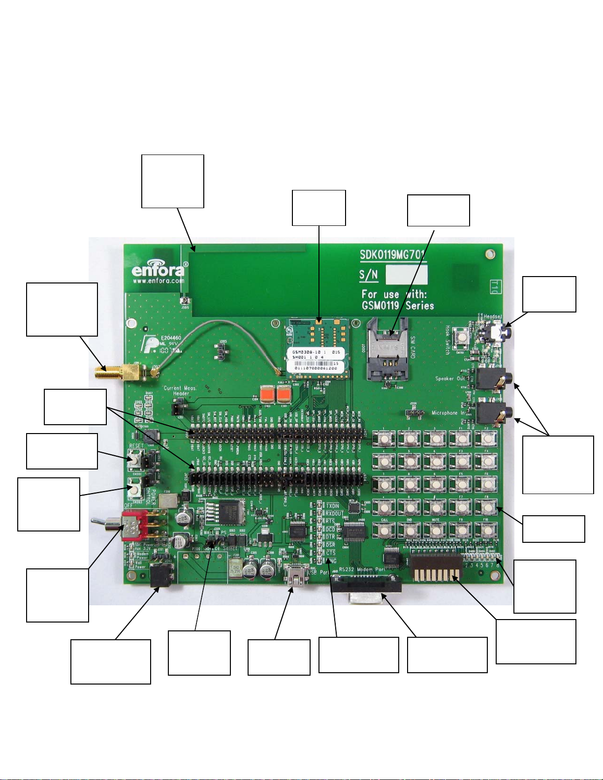
GSM/GPRS
Antenna
Connector
The Enfora SDK (Software Developer’s Kit) is designed to allow Enfora partners to
evaluate the Enfora Enabler III module and develop their own applications that will use
the Enfora Enabler module.
Quad Band
GSM/GPR
S Antenna
Enabler
Module
SIM
Holder
Headset
Jack
SW201
Reset*
SW203
PWR
CNTL
SW200
Power
Switch
Debug
Headers
Power Input
Port
J204 Power
Source
Select
Mini USB
Serial Port
Status LED’s
DB-9 Serial
Connection
Handset
Speaker and
Microphone
Jacks
Keyboard*
GPIO
Status
LED’s
GPIO DIP
Switch
Figure 1 SDK0119 Development Board
*Implementation varies – see table
Page 3

Switches and Jumpers
Switch Functionality Default Position
SW200 Turn modem power on from
power connectors J202 or
P200
Off - Once a power supply
has been applied to J202 or
P200 it may be placed in the
on position to power on
SDK and/or modem
SW201 Momentary switch:
Temporarily applies ground
to the ON_\OFF pin and
resets the modem.
SW203 Momentary switch:
temporarily applies ground
to \PWR ON pin (pin 35 of
When using early versions
of GSM0308 module (ID
061220 and prior), RESET
is not supported
N/A; J200 must be removed
to manually control
\PWR_ON (pin 35)
modem)
SW401 GPIO DIP Switch Up is
All switches open
open, down is closed
J200 \PWR_ON jumper, if
Jumper installed
installed, ground will
always be applied to Pin 35
of the modem,
automatically powering on.
To manually control
\PWR_ON, remove jumper
and control with SW203
J203 Selects assertion level of
reset function (SW201)
Default position of J203
shown. Alternate position is
not supported.
J204 Switches main power
To the left - using J202
source between J202 (to the
left) and P200 (right)
J301 Current measurement
Jumper installed
header. Remove jumper to
facilitate current
measurement of modem
NOTE: If using SDK0119MG700 and module marked PCBGSM0119MG902 or later,
you must remove R200 located next to SW201 (RESET) else the module will be
held in permanent reset. There is no reset supported with this combination of
hardware.
Page 4

RF connector
There are two RF cable assemblies. An SMA Connector has been provided to facilitate
using an external antenna (or port to test equipment) as well as an RF cable assembly
connecting an internal quad band antenna.
External SIM Connector
An external SIM connector is provided on the SDK. Users may use either the external
SIM or a SIM connector on the module (if configured), but not both at the same time.
The SIM CLOCK, control and data lines are physically the same lines that go to the on
board SIM. SIM’s cannot be installed both on the external SIM connector and the on
board SIM connector. It must be one or the other.
Audio Section
The audio section has a 4-pole stereo headset connector (J700) and separate speaker and
microphone handset connectors (J702 and J703). The audio path is configured with
AT$VSELECT command. AT$VSELECT=0 selects handset and AT$VSELECT=1
selects headset. Please see the AT command manual for the audio level commands.
GPIO Section
DIP switches and LED’s have been provided to help facilitate testing of GPIO and GPIO
based events. Each GPIO is tied to a DIP switch (SW401) and pulled up high through a
resistor. If the GPIO is configured as an input (See AT$IOCFG), a high or low can be
applied to each GPIO line by setting the corresponding DIP switch to open or closed. If
it is open, the line will be pulled high. If it is closed the line will be pulled low.
Each GPIO line also has a corresponding LED. These LED’s show the current state of
the GPIO. The opposite side of the LED is tied to ground. If the LED is illuminated,
then the GPIO line is high. If it is not illuminated, then the GPIO line is low
Serial Ports
The SDK has a standard serial port and USB serial debug port. The RS232 modem port
(J601) is the modem primary serial port. Prior to RS 232 conversion, each hardware line
is tied to a status LED. On the opposite side of the LED, each is tied to ground. If the
LED is illuminated the line is high, if it is not illuminated, the line is low.
The debug USB serial port (J600) is used for modem debugging and is for Enfora use
only. There is no control of the modem through the debug serial port.
Power Input Port
J202 is the power input port. The connector is of size 1.3mm inner and 3.8mm outer.
Centre pin is positive. Power supply input range is 4.5V – 9V maximum.
Debug headers
J400, J401, J403 and J404, located in the center of the board, bring each line from the
100-pin connector to a header pin, for ease of monitoring and troubleshooting.
Page 5

To use some features on the SDK, jumpers must be placed on the debug headers to link in
the feature. Removal of the jumper will isolate the SDK feature from the module to
allow for external circuitry to be added via the headers without interference from the
SDK.
The Factory Default for the Debug header jumper settings are: (all other pins are not
jumpered)
J401:
LED_A > LEDA_J
VRWLED > VRWLEDJ
J403:
USB_VBUS > USB_VBUS_J
DTR > DTR_J
CTS > CTS_J
RTS > RTS_J
TX > TX_J
DSR > DSR_J
DCD > DCD_J
RX > RX_J
RING > RING_J
I2C_DA > I2CDA
I2C_CK > I2CCK
_VBAK > VBAK
J404:
KBR0 > _KBR0
KBR1 > _KBR1
KBR2 > _KBR2
KBR3 > _KBR3
KBR4 > _KBR4
KBC0 > _KBC0
KBC1 > _KBC1
KBC2 > _KBC2
KBC3 > _KBC3
KBC4 > _KBC4
VRIO > VRIO_J
AX3V3 > COM_E
USBBT > GND
Page 6
Configuring the Enfora module
To communicate with, and configure the Enfora module, connect the serial connector of
the SDK to the serial port of a PC. From a Windows PC, you can use HyperTerminal to
configure the module. Please follow these instructions to correctly configure
HyperTerminal:
a. Start HyperTerminal
On Windows XP, click on:
Start>Programs>Accessories>Communications>HyperTerminal
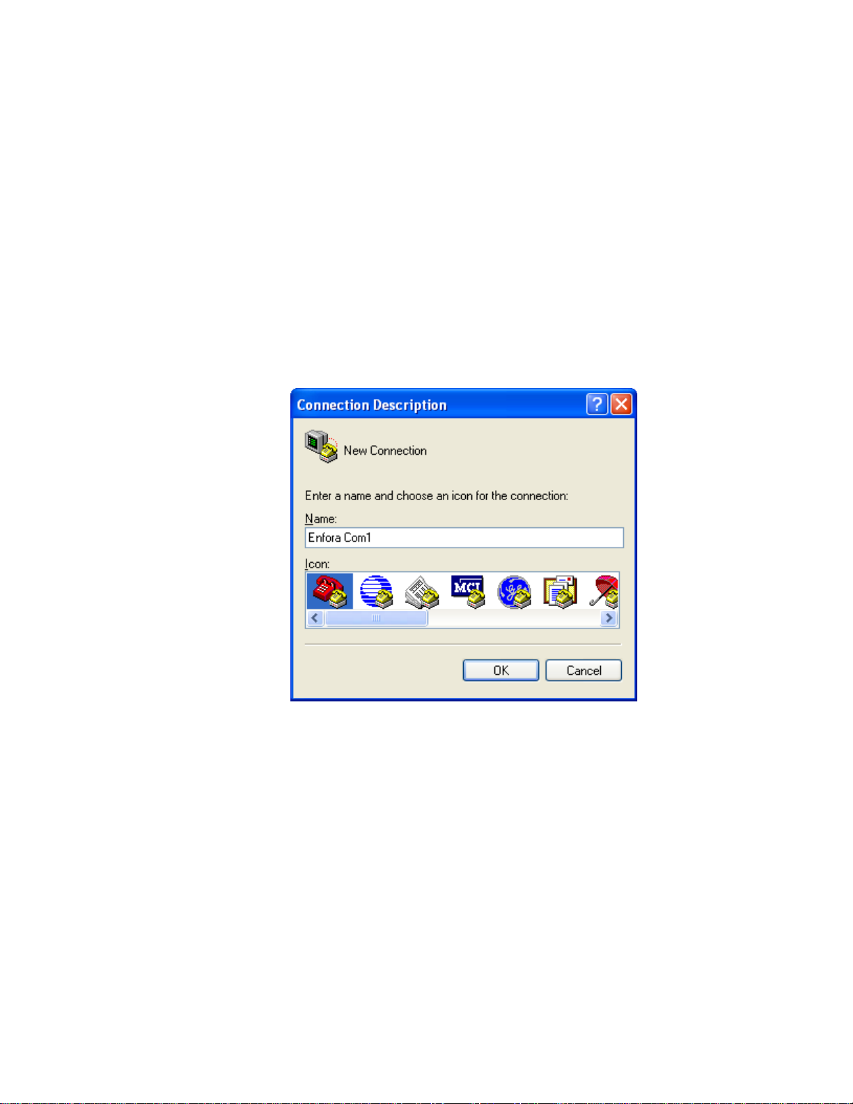
1. You should see the following screen.
2. Enter a name for the Connection. In this example, the Name is
Enfora Com1.
3. Click OK.
4. The next window that will appear is the Connect To window.
Page 7
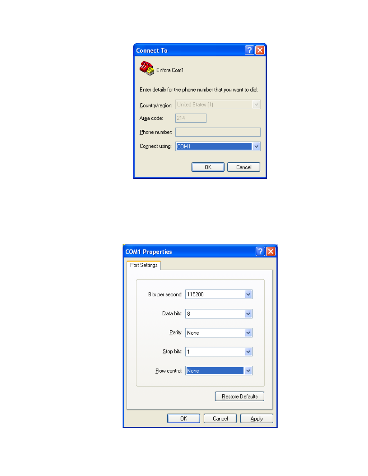
5. Change the Connect Using setting to the Com port that was
determined in Step 2.
6. Click OK.
7. The next window is the Port Settings window.
Page 8
8. Make sure the settings match the example.
9. Click OK.
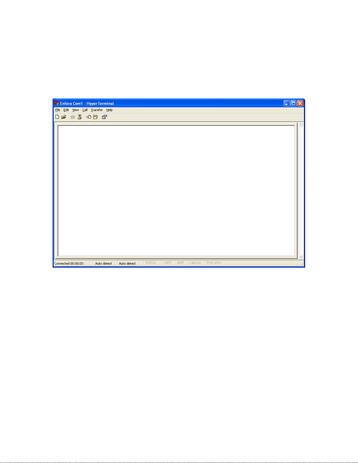
10. Now the Main Program Window should appear.
11. Terminal Setup Testing.
a. Make sure the cursor is in the main window.
b. Type “AT” and press “Enter”
c. You should see the modem respond back with “OK” in the
Main Window
d. If this happens, the COM port is configured correctly.
e. At this point you are ready to start configuring your SDK with
AT commands.
Page 9

Modem Settings that Allow for Automated GSM and GPRS Network Connectivity
1. Open the HyperTerminal connection that you configured in the previous section.
2. Type AT and press <ENTER> the modem should respond with OK. This will
verify that you are communicating with the modem. If you cannot see characters
entered on the screen, enter ATE1V1.
3. To perform a PDP context activation on a network, the following commands need
to be used:
AT&F (Default configuration)
AT+CREG=2 (status GSM registration)
AT%CGREG=2 (Status GPRS attach)
AT+CGDCONT=1,"IP","APN","",0,0 (.APN value will be provided by carrier. )
AT%CGPCO=1,"username,password",1 (Set Type of Authentication, Username and
Password if is need it)
AT+CPIN="xxxx" (xxx is a PIN number for SIM card if
needed)
AT$AREG=2 (auto GPRS activation on power up of
device)
AT&W (save the configuration)
SDK Tips
Before using the SDK for the first time, please make sure you remove all packing
material from the SDK (tape, etc.).
Enfora Parts
The SDK includes: The SDK Board and AC/DC “Wall-Pack” Power Supply. (Note:
The AC/DC Adapter is only supplied in the United States.)
There are optional accessories that you may need in addition to the Enfora module. Some
examples of these accessories are listed below. Please contact your Enfora sales
representative for specific part information, and ordering information.
• Molex Connector
• SIM Card Holder
User Manuals
GSM0308AT001.pdf – Enabler IIIG AT Command Set
GSM0308IG001.pdf - Enabler IIIG Integration Guide
Page 10

Schematic diagram
SDK0119MG801 - Enabler IIIG SDK Schematic Diagram
 Loading...