


 Loading...
KB9012
Keyboard Controller
Data Sheet
Revision 0.9
June 2010
ENE RESERVES THE RIGHT TO AMEND THIS DOCUMENT WITHOUT NOTICE AT ANY TIME. ENE ASSUMES NO RESPONSIBILITY FOR ANY ERRORS APPEAR IN THE DOCUMENT, AND ENE DISCLAIMS ANY EXPRESS OR IMPLIED WARRANTY, RELATING TO SALE AND/OR USE OF ENE PRODUCTS INCLUDING LIABILITY OR WARRANTIES RELATING TO FITNESS FOR A PARTICULAR PURPOSE, OR INFRINGEMENT OF ANY PATENTS, COPYRIGHTS OR OTHER INTELLECTUAL PROPERTY RIGHTS.
Headquarters |
Taipei Office |
4F-1, No.9, Prosperity Rd., |
4F, No.88, Bauchiau Rd. |
Science-based Industrial Park, |
Shindian City, Taipei, |
Hsinchu City, Taiwan, R.O.C |
Taiwan, R.O.C. |
TEL: 886-3-6662888 |
TEL: 886-2-89111525 |
|
FAX: 886-2-89111523 |
|
|
Copyright© 2011, ENE Technology Inc. All rights reserved. |
|
KB9012 Keyboard Controller Datasheet
ENE Technology Inc.
Confidential Document
Restricted Circulation
|
CONFIDENTIAL |
|
- |
This document is issued for |
only. Please do not transfer it to other companies. |
- This document is the property of ENE Technology Corp. It should be returned once unused. |
||
- |
Please do not make any copy of this document and deliver to others. |
|
THIS DOCUMENT CONTAINS CONFIDEMTIAL INFORMATION OF ENE PRODUCTS. ANY UNAUTHORIZED USE OR DISCLOSURE COULD
IMPACT ENE’S COMPETITIVE ADVANTAGE.
This document issued to:
Recipient
Company
Serial Number
Copyright© 2011, ENE Technology Inc. |
ii |

|
|
|
|
KB9012 Keyboard Controller Datasheet |
|||
|
|
Revision |
|
|
|
||
|
Revision |
|
Description |
Date |
|
||
|
0.1 |
|
1. |
Draft with only pin-assignment and IO cells |
2010/5 |
|
|
|
0.2 |
|
1. |
Re-organize contents, |
2010/6 |
|
|
|
|
|
2. |
Update IO cell name / structure |
|
|
|
|
|
|
3. Update Memory Map |
|
|
|
|
|
|
|
4. |
Reserved all electronic character for design characteristic only |
|
|
|
|
0.3 |
|
1. |
Update IO cell drive |
2010/6 |
|
|
|
0.4 |
|
1. |
Update Block Diagram with GWG |
2010/10 |
|
|
|
|
|
2. |
Correct IO cells typo, remove BQCZT04HIV |
|
|
|
|
|
|
3. |
Update power-fail flag in application appendix |
|
|
|
|
|
|
4. |
Update Register files as following : |
|
|
|
|
|
|
5. Update IKB HW command brief |
|
|
|
|
|
|
|
6. |
Update Open-Drain PWM register |
|
|
|
|
|
CONFIDENTIAL |
|
||||
|
|
|
7. |
Modify SHDI registers for fixed clock source, SHI modes |
|
|
|
|
|
|
8. |
Update WDT registers breathe LED flexible configuration |
|
|
|
|
|
|
9. |
Update LPC MEM cycle map to XRAM illustration |
|
|
|
|
|
|
10. Update XBI for e-flash operation and remove SHC description |
|
|
|
|
|
|
|
11. Update GWG register as new-added functions |
|
|
|
|
|
|
|
12. Update EC section registers for VC/PLC/ADC |
|
|
|
|
|
|
|
13. Update SMB, extend previously banked-REGs, slave address |
|
|
|
|
|
|
|
14. Update power-latch&voltage comparator in application appendix |
|
|
|
|
|
0.5 |
|
1. Update STOP mode power consumption |
2010/10 |
|
|
|
|
|
|
2. Add KBC POR and ECRST# timing |
|
|
|
|
|
0.6 |
|
1. Update KB9012 A1 P/N |
2010/12 |
|
|
|
|
0.7 |
|
1. |
Fix register typo, TCON W0C |
2011/01 |
|
|
|
|
|
2. |
Update PCON2 description |
|
|
|
|
|
|
3. |
Update GPIO MISC for SHDI pin-out enable for each ports |
|
|
|
|
|
|
4. |
Fix WDTCFG description of WDT disable password |
|
|
|
|
|
|
5. |
Update SHDI clock setting |
|
|
|
|
|
|
6. |
Update XBIMISC IC trimming status |
|
|
|
|
0.8 |
|
1. |
Update PS/2 Timing |
2011/03 |
|
|
|
|
|
2. |
Remove external SPI flashing timing |
|
|
|
|
|
|
3. |
Update BQCZT04IV cell character |
|
|
|
|
|
|
4. |
Update ESD information |
|
|
|
|
|
|
5. |
Update thermal information |
|
|
|
|
|
|
6. |
Update 9012A2 into P/N list and VC related setting. Please refer |
|
|
|
|
|
|
ECN for details. |
|
|
|
|
|
0.9 |
|
1. |
Update 9012A3 into P/N list and related changes. Please refer |
2011/06 |
|
|
|
|
|
ECN for details. |
|
|
|
|
|
|
|
2. Remove 4.13.3 & 4.13.4 LPC/FWH Memory decode range ; |
|
|
|
|
|
|
|
remove Bank0 0xFE90[3], 0xFE94[7:0], 0xFE95[2],[7] |
|
|
|
|
|
|
|
Bank1 0xFE92[5:0], 0xFE93[5:0] |
|
|
|
|
|
|
|
3. |
Refine WDT breath LED similar to non-embedded-flash product |
|
|
|
|
|
|
4. |
Refine ECMISC, IOSCCR for power consumption control |
|
|
|
|
|
|
5. |
Refine function select control of tables |
|
|
|
|
|
|
SDI host two ports select is by GPIO MISC[2:1] |
|
|
|
|
|
|
|
GPIO5D/5E (Crystal) is by CLK32CR[5:4] |
|
|
|
|
|
|
|
VCouts are by GPIOFSx |
|
|
|
|
|
|
|
Vcins are by VCCR[1:0] |
|
|
|
|
|
|
|
6. |
Revise application appendix to correspond latest setting |
|
|
|
|
1.0 |
|
1. |
Refine hardware trap section, recover FDA trap in A3 version |
2011/06 |
|
|
Copyright© 2011, ENE Technology Inc. |
i |

|
KB9012 Keyboard Controller Datasheet |
|
CONTENT |
|
|
CONTENT ................................................................................................................... |
|
II |
1. GENERAL DESCRIPTION..................................................................................... |
|
0 |
1.1 OVERVIEW ........................................................................................................... |
|
0 |
1.2 FEATURES ........................................................................................................... |
|
1 |
1.3 COMPARISON (KB930 VS. KB9012) .................................................................... |
|
6 |
CONFIDENTIAL |
||
1.4 BLOCK DIAGRAM ................................................................................................. |
|
7 |
2. PIN ASSIGNMENT AND DESCRIPTION .............................................................. |
|
8 |
2.1 KB9012 128-PIN LQFP DIAGRAM TOP VIEW....................................................... |
8 |
|
2.2 KB9012 128 LFBGA BALL MAP ........................................................................ |
|
9 |
2.3 KB9012 PIN ASSIGNMENT SIDE A ..................................................................... |
|
10 |
2.4 KB9012 PIN ASSIGNMENT SIDE B ...................................................................... |
|
11 |
2.5 KB9012 PIN ASSIGNMENT SIDE C ..................................................................... |
|
12 |
2.6 KB9012 PIN ASSIGNMENT SIDE D ..................................................................... |
|
13 |
2.7 I/O CELL DESCRIPTIONS .................................................................................... |
|
14 |
2.7.1 I/O Buffer Table ....................................................................................... |
|
14 |
2.7.2 I/O Buffer Characteristic Table.............................................................. |
|
14 |
3. PIN DESCRIPTIONS ............................................................................................ |
|
15 |
3.1 HARDWARE TRAP .............................................................................................. |
|
15 |
3.2 PIN DESCRIPTIONS BY FUNCTIONS ..................................................................... |
|
16 |
3.2.1 Low Pin Count I/F Descriptions. |
........................................................... |
16 |
3.2.2 PS/2 I/F Descriptions.............................................................................. |
|
16 |
3.2.3 Internal Keyboard Encoder (IKB) Descriptions .................................. |
16 |
|
3.2.4 SMBus Descriptions............................................................................... |
|
16 |
3.2.5 FAN Descriptions.................................................................................... |
|
17 |
3.2.6 Pulse Width Modulation (PWM) Descriptions..................................... |
17 |
|
3.2.7 Analog-to-Digital Converter Descriptions ........................................... |
17 |
|
3.2.8 Digital-to-Analog Converter Descriptions ........................................... |
17 |
|
3.2.9 8051 External I/F Descriptions .............................................................. |
|
17 |
3.2.10 External Clock Descriptions ............................................................... |
|
18 |
3.2.11 Miscellaneous Signals Descriptions .................................................. |
18 |
|
3.2.12 Voltage Comparator Pins Descriptions ............................................. |
18 |
|
3.2.13 Power Pins Descriptions ..................................................................... |
|
18 |
3.2.14 51ON Power Pins Descriptions .......................................................... |
19 |
|
Copyright© 2011, ENE Technology Inc. |
ii |
|

|
KB9012 Keyboard Controller Datasheet |
|
4. MODULE DESCRIPTIONS .................................................................................. |
|
20 |
4.1 CHIP ARCHITECTURE ......................................................................................... |
|
20 |
4.1.1 Power Planes........................................................................................... |
|
20 |
4.1.2 Clock Domains ........................................................................................ |
|
21 |
4.1.3 PCICLK and CLKRUN#........................................................................... |
|
23 |
4.1.4 Internal Memory Map.............................................................................. |
|
24 |
4.2 GPIO ................................................................................................................ |
|
25 |
4.2.1 GPIO Function Description ................................................................... |
|
25 |
CONFIDENTIAL |
||
4.2.2 GPIO Structures ...................................................................................... |
|
29 |
4.2.3 GPIO Attribution Table ........................................................................... |
|
30 |
4.2.4 GPIO Registers Descriptions (0xFC00~0xFC7F) ................................ |
33 |
|
4.2.5 GPIO Programming Sample .................................................................. |
|
48 |
4.3 KEYBOARD AND MOUSE CONTROL INTERFACE (KBC) ........................................ |
49 |
|
4.3.1 KBC I/F Function Description ............................................................... |
|
49 |
4.3.2 KBC Registers Description (0xFC80~0xFC8F) ................................... |
50 |
|
4.4 ENE SERIAL BUS CONTROLLER (ESB).............................................................. |
|
54 |
4.4.1 ESB Function Description ..................................................................... |
|
54 |
4.4.2 ESB Registers Description (0xFC90~0xFC9F) ................................... |
55 |
|
4.4.3 ESB Programming Sample.................................................................... |
|
60 |
4.5 INTERNAL KEYBOARD (IKB) ENCODER .............................................................. |
|
61 |
4.5.1 IKB Function Description ...................................................................... |
|
61 |
4.5.2 IKB Registers Description (0xFCA0~0xFCAF).................................... |
63 |
|
4.5.3 IKB Matrix Value Mapping Table ........................................................... |
69 |
|
4.6 PECI................................................................................................................. |
|
72 |
4.6.1 PECI Functional Description ................................................................. |
|
72 |
4.6.2 PECI Timing Setting ............................................................................... |
|
73 |
4.6.3 PECI Register Description (0xFCD0~0xFCDF) ................................... |
74 |
|
4.7 OWM ................................................................................................................ |
|
78 |
4.7.1 OWM Functional Description ................................................................ |
|
78 |
4.7.2 OWM Timing Setting Illustration .......................................................... |
79 |
|
4.7.3 OWM Register Description (0xFCF0~0xFCFF) ................................... |
80 |
|
4.8 PULSE WIDTH MODULATION (PWM) .................................................................. |
|
83 |
4.8.1 PWM Function Description.................................................................... |
|
83 |
4.8.2 PWM Duty Cycle Setting Illustration .................................................... |
84 |
|
4.8.3 PWM Registers Description (0xFE00~0xFE1F) .................................. |
87 |
|
4.9 FAN CONTROLLER ............................................................................................. |
|
90 |
Copyright© 2011, ENE Technology Inc. |
iii |
|

|
KB9012 Keyboard Controller Datasheet |
|
4.9.1 Fan Function Description ...................................................................... |
|
90 |
4.9.1.1 Fan Tachometer Monitor & Auto-FAN mode .................................... |
91 |
|
4.9.1.2 FANPWM Setting & Fixed-FAN Mode................................................ |
92 |
|
4.9.2 Fan Registers Description (0xFE20~0xFE4F) ..................................... |
93 |
|
4.9.3 Fan Programming Sample..................................................................... |
|
99 |
4.10 GENERAL PURPOSE TIMER (GPT) ................................................................. |
|
100 |
4.10.1 GPT Function Description ................................................................. |
|
100 |
4.10.2 GPT Registers Description (0xFE50~0xFE6F) ................................ |
101 |
|
CONFIDENTIAL |
||
4.10.3 GPT Programming Sample................................................................ |
|
103 |
4.11 SDI HOST/DEVICE INTERFACE CONTROLLER .................................................. |
104 |
|
4.11.1 SDI Host/Device Interface Description............................................. |
104 |
|
4.11.2 SDI Host Interface Register Description (0xFE70~0xFE7F) .......... |
106 |
|
4.11.3 SDI Device Interface Register Description (0xFE70~0xFE7F) ...... |
108 |
|
4.11.4 SDI Programming Sample .................................................................. |
|
111 |
4.12 WATCHDOG TIMER (WDT) ............................................................................. |
|
112 |
4.12.1 WDT Function Description ................................................................ |
|
112 |
4.12.2 Setting for WDT Breathing LED ........................................................ |
113 |
|
4.12.3 WDT Registers Description (0xFE80~0xFE8F) ............................... |
114 |
|
4.12.4 WDT Programming Sample............................................................... |
|
118 |
4.13 LOW PIN COUNT INTERFACE (LPC)................................................................ |
|
119 |
4.13.1 LPC Function Description ................................................................. |
|
119 |
4.13.2 LPC I/O Decode Range ...................................................................... |
|
119 |
4.13.3 Index-I/O Port ...................................................................................... |
|
120 |
4.13.4 LPC to MEM cycle XRAM................................................................... |
|
121 |
4.13.5 Extended I/O Port (Debug Port, Port80) .......................................... |
123 |
|
4.13.6 LPC Registers Description (0xFE90~0xFE9F for bank selection) 124 |
||
4.14 X-BUS INTERFACE (XBI)................................................................................ |
|
132 |
4.14.1 XBI Function Description .................................................................. |
|
132 |
4.14.2 XBI Registers Description (0xFEA0~0xFEBF) ................................ |
133 |
|
4.15 CONSUMER IR CONTROLLER (CIR)................................................................ |
|
138 |
4.15.1 CIR Function Description .................................................................. |
|
138 |
4.15.2 CIR Block Diagram ............................................................................. |
|
140 |
4.15.3 CIR Remote Protocol.......................................................................... |
|
141 |
4.15.3.1 Philips RC5 Protocol........................................................................................ |
|
141 |
4.15.3.2 Philips RC6 Protocol........................................................................................ |
|
142 |
4.15.3.3 NEC Protocol.................................................................................................... |
|
142 |
4.15.4 CIR Automatic Carrier Frequency Detection and Modulation ...... |
143 |
|
Copyright© 2011, ENE Technology Inc. |
iv |
|

|
KB9012 Keyboard Controller Datasheet |
|
4.15.5 CIR Registers Description (0xFEC0~0xFECF) ................................ |
145 |
|
4.15.6 CIR Programming Sample ................................................................. |
149 |
|
4.16 GENERAL WAVEFORM GENERATOR (GWG) ................................................... |
150 |
|
4.16.1 GWG Function Description ............................................................... |
150 |
|
4.16.2 GWG Register Description (0xFED0~0xFEDF) ............................... |
151 |
|
4.17 PS/2 INTERFACE (PS/2) ................................................................................ |
|
153 |
4.17.1 PS/2 Interface Function Description ................................................ |
153 |
|
4.17.2 PS/2 Interface Registers Description (0xFEE0~0xFEFF) .............. |
153 |
|
CONFIDENTIAL4.20.3 SMBus Controller 1 Register Description (0xFFD0~0xFFFF) ....... 196 |
||
4.18 EMBEDDED CONTROLLER |
(EC) ...................................................................... |
157 |
4.18.1 EC Function Description ................................................................... |
157 |
|
4.18.2 EC Command Program Sequence.................................................... |
158 |
|
4.18.3 EC SCI Generation |
.............................................................................. |
159 |
4.18.4 EC/KBC Clock Configuration ............................................................ |
160 |
|
4.18.5.1 A/D Converter Control..................................................................... |
161 |
|
4.18.5.2 A/D Panel Drive Mode ..................................................................... |
162 |
|
4.18.6 D/A Converter Control........................................................................ |
163 |
|
4.18.7 Power Management Control.............................................................. |
164 |
|
4.18.8 EC Registers Description (0xFF00~0xFF2F) ................................... |
165 |
|
4.19 GENERAL PURPOSE WAKE-UP CONTROLLER (GPWU)................................... |
177 |
|
4.19.1 GPWU Function Description ............................................................. |
177 |
|
4.19.2 GPWU Registers Description (0xFF30~0xFF7F) ............................ |
178 |
|
4.19.3 GPWU Programming Sample............................................................ |
187 |
|
4.20 SYSTEM MANAGEMENT BUS CONTROLLER (SMBUS) ..................................... |
188 |
|
4.20.1 SMBus Function Description ............................................................ |
188 |
|
4.20.2 SMBus Controller 0 Register Description (0xFF90~0xFFBF) ....... |
192 |
|
4.21 8051 MICROPROCESSOR ............................................................................... |
|
201 |
4.21.1 8051 Microprocessor Function Description ................................... |
201 |
|
4.21.2 8051 Microprocessor Instruction ..................................................... |
202 |
|
4.21.3 8051 Interrupt Controller ................................................................... |
207 |
|
4.21.4 Interrupt Enable/Flag Table............................................................... |
208 |
|
4.21.5 8051 Special Function Register (SFR) ............................................. |
210 |
|
4.21.6 8051 Microprocessor Register Description .................................... |
211 |
|
APPLICATION APPENDIX : .................................................................................. |
|
218 |
A.1 ENE DEBUG INTERFACE, EDI .......................................................................... |
218 |
|
A.1.1 Enable EDI............................................................................................. |
|
219 |
Copyright© 2011, ENE Technology Inc. |
v |
|

|
|
KB9012 Keyboard Controller Datasheet |
A.1.2 EDI Instructions.................................................................................... |
|
219 |
A.1.3 Read Command.................................................................................... |
|
220 |
A.1.4 Write Command.................................................................................... |
|
220 |
A.1.5 Disable EDI Command......................................................................... |
|
221 |
A.2 POWER-LATCH ................................................................................................ |
|
222 |
A.3 VOLTAGE COMPARATOR .................................................................................. |
|
223 |
A.4 POWER FAIL FLAG BRIEF DESCRIPTION........................................................... |
|
225 |
CONFIDENTIAL |
||
A.5 EMBEDDED FLASH BRIEF DESCRIPTION........................................................... |
|
226 |
5. ELECTRICAL CHARACTERISTICS ................................................................. |
|
227 |
5.1 ABSOLUTE MAXIMUM RATING........................................................................... |
|
227 |
5.2 DC ELECTRICAL CHARACTERISTICS ................................................................. |
|
227 |
BQCZ16HIV ..................................................................................................... |
|
227 |
BQC04HIV ....................................................................................................... |
|
227 |
BQCW16HIV .................................................................................................... |
|
228 |
BQC04HI .......................................................................................................... |
|
228 |
BQC08HIV ....................................................................................................... |
|
228 |
BQC04HIVPECI............................................................................................... |
|
229 |
BQCZT04IV (XCLKI, XCLKO, ADC/DAC) |
..................................................... 230 |
|
5.3 A/D & D/A CHARACTERISTICS ......................................................................... |
|
231 |
5.4 RECOMMEND OPERATION CONDITION ............................................................... |
|
232 |
5.5 OPERATING CURRENT ...................................................................................... |
|
232 |
5.6 PACKAGE THERMAL INFORMATION ................................................................... |
|
232 |
5.7 AC ELECTRICAL CHARACTERISTICS ................................................................. |
|
233 |
5.7.1 KBC POR and ECRST# ........................................................................ |
|
233 |
5.7.2 LPC interface Timing............................................................................ |
|
234 |
5.7.3 PS/2 interface Timing ........................................................................... |
|
236 |
5.7.4 SMBus interface Timing....................................................................... |
|
237 |
6. PACKAGE INFORMATION................................................................................ |
|
238 |
6.1 LQFP 128-PIN OUTLINE DIAGRAM .................................................................. |
|
238 |
6.1.1 Top View................................................................................................. |
|
238 |
6.1.2 Side View ............................................................................................... |
|
239 |
6.1.3 Lead View............................................................................................... |
|
240 |
6.1.4 LQFP Outline Dimensions ................................................................... |
|
241 |
6.2 LFBGA 128-PIN OUTLINE DIAGRAM ............................................................... |
|
242 |
6.2.1 Top View................................................................................................. |
|
242 |
6.2.2 Side View ............................................................................................... |
|
243 |
Copyright© 2011, ENE Technology Inc. |
vi |
|

|
KB9012 Keyboard Controller Datasheet |
6.2.3 Bottom View .......................................................................................... |
244 |
6.2.4 LFBGA Outline Dimensions ................................................................ |
245 |
6.3 PART NUMBER DESCRIPTION............................................................................ |
246 |
CONFIDENTIAL
Copyright© 2011, ENE Technology Inc. |
vii |
1. General Description
1.1 Overview
The ENE KB9012 is a customized IC based on KB9010 for specific application of minimizing power-consumption. Several pins are provided for external power-latch to save power-consumption. IO characteristic and cells are also improved.
The ENE KB901x series is embedded controller (EC) with embedded-Flash for notebook platforms. In KB9012, the e-Flash is 128KB. The embedded controller contains industrial standard 8051 microprocessor and provides function of i8042 keyboard controller basically. KB9012 is embedded LPC interface used to communicate with Host. The embedded controller also features rich interfaces for general applications, such as PS/2 interface, Keyboard matrix encoder, PWM controller, A/D converter, D/A converter, Fan controller, SMBus controller, GPIO controller, PECI controller, one wire master, SPI controller, and extended interface (ENE Serial Bus) for more applications, like capacitive touch button application and GPIO extender.
Compared with last generation of KB3926 series, KB9012 added PECI/OWM, another 2 SMBus, another 2 Fan tachometers, enhanced SPI host/slave controller, internal oscillator for newest application. KB9012 also improves structure of other modules including 8051, XBI, LPC, IKB, FAN, WDT, GPIO, ESB, EDI. For detail improvement, please refer the related section.
KB9012 Keyboard Controller Datasheet
1.2 Features
LPC Low Pin Count Interface
SIRQ supporting IRQ1, IRQ12, SCI or SMI# interrupt and one programmable IRQ provided.
I/O Address Decoding:
Legacy KBC I/O port 60h/64h
Programmable EC I/O port, 62h/66h(recommend)
I/O port 68h/6Ch (sideband)
2 Programmable 4-byte Index-I/O ports to access internal EC registers.
Memory Decoding:
Firmware Hub decode
LPC memory decode
Compatible with LPC specification v1.1
Support LPC interface re-direction to IKB for debugging
X-bus Bus Interface (XBI) : Flash Interface
Embedded 128KB flash support
The 64KB code memory can be mapped into system memory by one 16KB and one 48KB programmable pages independently.
Enhanced pre-fetch mechanism.
CONFIDENTIAL8051 Microprocessor
Compatible with industrial 8051 instructions with 3 cycles.
8051 runs at 8/16/22 MHz, programmable.
256 bytes internal RAM. (special design) and 4KB tight-coupled SRAM
24 extended interrupt sources.
Two 16-bit timers.
Supports idle and stop mode.
Enhanced embedded debug interface.
Support Tx/Rx and support re-direction to IKB for debugging
Copyright© 2011, ENE Technology Inc. |
1 |

KB9012 Keyboard Controller Datasheet
8042 Keyboard Controller
8 standard 8042 commands processed by hardware.
Each hardware command can be optionally processed by firmware.
Pointing device multiplex mode support.
Fast GA20 and KB reset support.
PS/2 Controller
CONFIDENTIAL Support at most 3 external PS/2 devices.
External PS/2 device operation in firmware mode.
Internal Keyboard Matrix (IKB)
18x8 keyboard scan matrix.
Support W2K Internet and multimedia keys.
Support hotkey events defined.
Ghost key cancellation mechanism provided.
Enhanced de-bounce feature added
Embedded Controller (EC)
ACPI Spec 2.0 compliant.
5 standard EC commands supported directly by hardware.
Each hardware command can be processed by firmware optionally.
Programmable EC I/O ports, 62h/66h by default.
SMBus Host Controller
4 SMBus Interfaces with 2 SMBus Controllers
SMBus Spec 2.0 compliant.
Byte mode support.
Slave function support.
Digital-to-Analog Converter (DAC)
4 DAC channels with 8-bit resolution.
All pins of DAC can be alternatively configured as GPIO.
Copyright© 2011, ENE Technology Inc. |
2 |

KB9012 Keyboard Controller Datasheet
Analog-to-Digital Converter (ADC)
8 ADC channels with 10-bit resolution.
All pins of ADC can be alternatively configured as GPIO.
Pulse Width Modulator (PWM)
6 PWM channels are provided. (8-bit *2, 14-bit *2 and FANPWM(12-bit) *2)
Clock source selectable:. CONFIDENTIAL 1MHz/64KHz/4KHz/256Hz (for 8-bit PWM)
Peripheral clock or 1MHz (for 14-bit PWM)
Peripheral clock (for FANPWM)
Duty cycle programmable and cycle time up to 1 sec(for 8-bit PWM)
WatchDog Timer (WDT)
32.768KHz input clock.
10-bit counter with 32ms unit for watchdog reset.
Three watchdog reset mechanism.
Reset 8051
Reset whole chip, except GPIO.
Reset whole chip including GPIO.
WDT breathing LED
Real Time Clock
32.768KHz input clock.
24-bit timer support.
General Purpose Timer (GPT)
Two 16-bit and two 8-bit general purpose timer with 32.768KHz clock source.
General Purpose Wakeup (GPWU)
Those I/O with GPI (general purpose input) configuration can generate interrupts or wakeup events, including pins named in GPXIOAxx.
Copyright© 2011, ENE Technology Inc. |
3 |

KB9012 Keyboard Controller Datasheet
General Purpose Input/Output (GPIO)
All general purpose I/O can be programmed as input or output.
All output pins can be configured to be tri-state optionally.
All input pins are equipped with pull-up, high/low active and edge/level trigger
selection.
All pins of DAC can be configured as GPIO.
All pins of ADC can be configured as GPIO.
|
A specific pair of GPIO pins with signal pass-through feature. |
CONFIDENTIAL |
|
|
GPIO50 for external lock signal set by firmware, un-locked by PCIRST# falling |
FAN Controller
Two fan controllers with tachometer inputs.
Automatic fan control support.
12-bit FANPWM support.
Consumer IR (CIR)
Several protocols decoded/encoded by hardware.
Interrupt for CIR application.
Support wide/narrow band receiver.
Transmit/Receive simultaneously.
Remote power-on support.
ENE Serial Bus Interface (ESB)
A proprietary and flexible interface for extension with ENE KBC.
Firmware accesses ESB devices via internal memory address directly.
Interrupt capability.
ENE Debug Interface (EDI)
Flexible debug interface with IKB pins.
Keil-C development tool compatible
EDI detect frequency support 1M~8M
SPI Device Interface (SHDI)
A enhanced SPI host/device controller is embedded in the KBC.
Flexible design for SPI applications.
One Wire Master (OWM)
Embedded One Wire controller used to control one wire devices.
Copyright© 2011, ENE Technology Inc. |
4 |

KB9012 Keyboard Controller Datasheet
PECI Interface
Support Intel PECI.
Support wide speed range from 2Kbps to 2Mbps.
Power Management
Sleep mode: 8051 program counter (PC) stops and enters idle mode.
Deep sleep mode: All clocks stop except external 32.768KHz OSC. 8051 enters stop mode.
51ON power management function
MISC
Support General Waveform Generator to easily and accurately generate us-scale to ms-scale specific waveform.
Support two voltage comparators. Two voltage input sources to compare with internal DAC voltage value, and response the comparison result on two digital
CONFIDENTIALoutputs, used to detect abnormal situation (like over temperature and etc.).
Package
128-pin LQFP package, Lead Free (RoHS).
Copyright© 2011, ENE Technology Inc. |
5 |

|
|
|
|
|
|
KB9012 Keyboard Controller Datasheet |
|||
|
1.3 Comparison (KB930 vs. KB9012) |
|
|
|
|
|
|||
|
|
|
|
|
|
|
|
|
|
|
|
|
|
KB930A |
|
|
KB9012 |
|
|
|
Microprocessor |
|
8051 (256byte IRAM) |
|
8051 (256byte IRAM) |
|
|||
|
Built-in SRAM |
|
4KB |
|
|
4KB |
|
|
|
|
LPC |
|
2 index-I/O sets |
|
2 index-I/O sets |
|
|
||
|
Flash |
|
None |
|
|
Embedded flash 128KB |
|
|
|
|
Real Time Clock |
|
support |
|
|
Support |
|
|
|
|
ADC |
|
Six 10-bit ADC channels |
|
Eight 10-bit ADC channels |
|
|
||
|
DAC |
|
Four 8-bit DAC channels |
|
Four 8-bit DAC channels |
|
|
||
|
WDT |
|
32ms timer unit with 10bits control |
|
32ms timer unit with 10bits control |
|
|
||
|
OWM |
|
Support |
|
|
Support |
|
|
|
|
|
CONFIDENTIAL51ON Power Management |
|
|
|||||
|
PWM |
|
6 sets |
|
|
6 sets |
|
|
|
|
|
|
PWM0/1 |
– 8 bit |
|
PWM0/1 |
– 8 bit |
|
|
|
|
|
|
|
|
||||
|
|
|
PWM2/3 |
– 14 bit |
|
PWM2/3 |
– 14 bit |
|
|
|
|
|
FANPWM0/1 – 12 bit |
|
FANPWM0/1 – 12 bit |
|
|||
|
External PS/2 I/F |
3 |
|
3 |
|
|
|
||
|
GPIO |
|
Programmable Bi-direction I/O |
|
Programmable Bi-direction I/O |
|
|
||
|
|
|
GPIO pass through : 1 pair |
|
GPIO pass through : 1 pair |
|
|
||
|
|
|
|
|
|
||||
|
|
|
Max 100 pins I/O |
|
Max 106 pins I/O |
|
|||
|
|
|
|
|
|
All GPIO are bi-directional |
|
||
|
|
|
|
|
|
All GPIO are wake-up enable |
|
||
|
IKB Matrix |
|
18x8 |
|
|
18x8 |
|
|
|
|
FAN controller |
|
2 (Enhanced precision and 2 |
|
2 (Enhanced precision and 2 |
|
|
||
|
|
|
additional Tachometer Monitors) |
|
additional Tachometer Monitors) |
|
|
||
|
GPT |
4 |
|
4 |
|
|
|
||
|
SMBus |
|
4 Interfaces with 2 controllers |
|
4 (F/W updated) |
|
|
||
|
|
|
Byte mode support |
|
Byte mode support |
|
|
||
|
|
|
|
|
|
||||
|
CIR |
|
Hardware encode/decode |
|
Hardware encode/decode |
|
|
||
|
|
|
IRQ and I/O port support |
|
IRQ and I/O port support |
|
|
||
|
|
|
Carrier frequency calculation |
|
Carrier frequency calculation |
|
|||
|
|
|
TX with carrier modulation |
|
TX with carrier modulation |
|
|||
|
|
|
Learning mode support |
|
Learning mode support |
|
|||
|
|
|
TX/RX simultaneously |
|
TX/RX simultaneously |
|
|||
|
PECI |
|
Support PECI 3.0 |
|
Support PECI 3.0 |
|
|
||
|
EDI |
|
Support |
|
|
Support |
|
|
|
|
ESB |
|
Support |
|
|
Support |
|
|
|
|
SDI/SHDI |
|
SDI Host/Slave support |
|
SDI Host/Slave support |
|
|
||
|
MISC |
|
Voltage Comparator |
|
Voltage Comparator (Different pin-out |
|
|
||
|
|
|
|
|
|
compared with KB930) |
|
|
|
|
|
|
|
|
|
|
|
||
|
|
|
|
|
|
General Waveform Generator |
|
||
|
|
|
|
|
|
|
|
|
|
|
Package |
|
128 LQFP |
|
|
128 LQFP |
|
|
|
|
Dimension |
|
14mmx14mm |
|
14mmx14mm |
|
|
||
Copyright© 2011, ENE Technology Inc. |
6 |

|
|
|
|
|
|
KB9012 Keyboard Controller Datasheet |
|
1.4 Block Diagram |
|
|
|
|
|||
|
|
|
|
|
|
8051 |
|
|
|
|
|
|
|
build-in with |
XBI/XIO |
|
|
|
LPC I/F |
|
2 16-bit timers |
||
|
|
|
|
|
|||
|
|
|
|
|
|
1 UART |
code |
|
|
|
|
|
24 extended interrupt channels |
||
|
|
|
|
|
Fetching |
||
|
|
|
|
|
|
|
|
|
|
|
|
|
|
|
Bus |
|
|
|
|
LPC/FWH |
Data |
|
|
|
|
|
|
|
|
||
|
|
|
|
MEM cycles |
Bus |
|
|
CONFIDENTIALx 10 |
|||||||
EDI |
|
|
|
|
ENE Host BUS |
|
|
|
|
|
EC |
|
|
|
SPI I/F |
|
KBC |
|
Port 80 |
|
|
|
|
IO Cycles |
|
Index |
|
|
|
|
|
|
|
IO Cycles |
|
|
|
|
|
|
|
|
|
GPIO |
GPT |
4KB |
PWM |
|
|
|
|
x 106 |
x 4 |
SRAM |
X 6 |
|
|
|
EC |
EC Index mode can accessing |
FAN |
||
|
|
|
hardware |
full register space by this path |
X 2 |
||
|
|
|
command |
||||
|
|
|
|
|
|
|
|
|
KBC |
x 5 |
|
|
|
|
|
|
hardware |
|
|
ADC |
DAC |
|
|
|
command |
|
|
|
|||
|
|
|
X 8 |
x 4 |
|
||
|
|
x 8 |
|
|
|
||
|
|
|
|
|
|
SHDI |
|
|
|
|
|
|
|
|
|
|
|
|
|
|
|
|
ENE |
|
|
|
|
|
|
|
2nd |
|
|
|
|
|
|
|
BUS |
|
IKB |
|
|
|
|
|
|
|
18 x 8 |
PMU |
|
|
GWG |
|
|
|
hardware |
|
|
|
|||
|
command |
|
|
|
|
|
|
PCI clock |
|
|
|
|
|
CIR |
SMBx2 |
|
|
|
|
|
|
||
|
|
|
|
|
|
ESB |
4 ports |
|
|
|
|
|
|
|
|
32.768 Mhz |
|
|
|
|
|
|
|
|
|
|
|
|
|
PECI |
|
16.384 Mhz |
PS2 |
clock |
|
|
OWM |
|
|
|
|
|
WDT |
||||
|
|
x 3 |
control |
|
|
||
|
|
|
|
|
|
||
32.768 Khz |
|
|
|
|
|
|
|
Copyright© 2011, ENE Technology Inc. |
7 |

KB9012 Keyboard Controller Datasheet
2.Pin Assignment and Description
2.1 KB9012 128-pin LQFP Diagram Top View
|
VCC GPIO56 |
GND GPIO55 |
GPIO54 |
GPIO53 |
GPIO52 |
GPIO50 |
PSDAT3 |
PSCLK3 |
PSDAT2 |
PSCLK2 |
PSDAT1 |
PSCLK1 |
KSO17 |
KSO16 |
SDA1 |
SCL1 |
SDA0 |
SCL0 |
AD5 |
AD4 |
AD7 |
AD6 |
DA3 |
DA2 |
DA1 |
AGND |
DA0 AVCC AD3 AD2 |
|
||||||
|
96 |
95 |
94 |
93 |
92 |
91 |
90 |
89 |
88 |
87 |
86 |
85 |
84 |
83 |
82 |
81 |
80 |
79 |
78 |
77 |
76 |
75 |
74 |
73 |
72 |
71 |
70 |
69 |
68 |
67 |
66 |
65 |
|
|
GPXIOA00 |
97 |
|
|
|
|
|
|
|
|
|
|
|
|
|
|
|
|
|
|
|
|
|
|
|
|
|
|
|
|
|
|
|
64 |
AD1 |
GPXIOA01 |
98 |
|
|
|
|
|
|
|
|
|
|
|
|
|
|
|
|
|
|
|
|
|
|
|
|
|
|
|
|
|
|
|
63 |
AD0 |
GPXIOA02 |
99 |
|
|
|
|
|
|
|
|
|
|
|
|
|
|
|
|
|
|
|
|
|
|
|
|
|
|
|
|
|
|
|
62 |
KSI7 |
GPXIOA03 |
100 |
|
|
|
|
|
|
|
|
|
|
|
|
|
|
|
|
|
|
|
|
|
|
|
|
|
|
|
|
|
|
|
61 |
KSI6 |
GPXIOA04 |
101 |
|
|
|
|
|
|
|
|
|
|
|
|
|
|
|
|
|
|
|
|
|
|
|
|
|
|
|
|
|
|
|
60 |
KSI5 |
GPXIOA05 |
102 |
|
|
|
|
|
|
|
|
|
|
|
|
|
|
|
|
|
|
|
|
|
|
|
|
|
|
|
|
|
|
|
59 |
KSI4 |
GPXIOA06 |
103 |
|
|
|
|
|
|
|
|
|
|
|
|
|
|
|
|
|
|
|
|
|
|
|
|
|
|
|
|
|
|
|
58 |
KSI3 |
GPXIOA07 |
104 |
|
|
|
|
|
|
|
|
|
|
|
|
|
|
|
|
|
|
|
|
|
|
|
|
|
|
|
|
|
|
|
57 |
KSI2 |
GPXIOA08 |
105 |
|
|
|
|
|
|
|
|
|
|
|
|
|
|
|
|
|
|
|
|
|
|
|
|
|
|
|
|
|
|
|
56 |
KSI1 |
GPXIOA09 |
106 |
|
|
|
|
|
|
|
|
|
|
|
|
|
|
|
|
|
|
|
|
|
|
|
|
|
|
|
|
|
|
|
55 |
KSI0 |
GPXIOA10 |
107 |
|
|
|
|
|
|
|
|
|
KB9012 |
|
|
|
|
|
|
|
|
54 |
KSO15 |
|||||||||||||
GPXIOA11 |
108 |
|
|
|
|
|
|
|
|
|
|
|
|
|
|
|
|
|
53 |
KSO14 |
||||||||||||||
GPXIOD00 |
109 |
|
|
|
|
|
|
|
|
|
|
|
|
|
|
|
|
|
52 |
KSO13 |
||||||||||||||
GPXIOD01 |
110 |
|
|
|
|
|
|
|
|
|
|
|
|
|
|
|
|
|
51 |
KSO12 |
||||||||||||||
VCC 0 |
111 |
|
|
|
|
|
|
|
128-LQFP |
|
|
|
|
|
|
50 |
KSO11 |
|||||||||||||||||
GPXIOD02 |
112 |
|
|
|
|
|
|
|
|
|
|
|
|
|
49 |
KSO10 |
||||||||||||||||||
GND 0 |
113 |
|
|
|
|
|
|
|
|
|
|
|
|
|
48 |
KSO9 |
||||||||||||||||||
GPXIOD03 |
114 |
|
|
|
|
|
|
|
|
|
|
|
|
|
47 |
KSO8 |
||||||||||||||||||
|
|
|
|
|
|
|
|
|
|
|
|
|
|
|
|
|
|
|
|
|
|
|
|
|
|
|
|
|
|
|
||||
GPXIOD04 |
115 |
|
|
|
|
|
|
|
|
|
|
|
|
|
|
|
|
|
|
|
|
|
|
|
|
|
|
|
|
|
|
|
46 |
KSO7 |
GPXIOD05 |
116 |
|
|
|
|
|
|
|
|
|
|
|
|
|
|
|
|
|
|
|
|
|
|
|
|
|
|
|
|
|
|
|
45 |
KSO6 |
GPXIOD06 |
117 |
|
|
|
|
|
|
|
|
|
|
|
|
|
|
|
|
|
|
|
|
|
|
|
|
|
|
|
|
|
|
|
44 |
KSO5 |
GPXIOD07 |
118 |
|
|
|
|
|
|
|
|
|
|
|
|
|
|
|
|
|
|
|
|
|
|
|
|
|
|
|
|
|
|
|
43 |
KSO4 |
GPIO5B |
119 |
|
|
|
|
|
|
|
|
|
|
|
|
|
|
|
|
|
|
|
|
|
|
|
|
|
|
|
|
|
|
|
42 |
KSO3 |
GPIO5C |
120 |
|
|
|
|
|
|
|
|
|
|
|
|
|
|
|
|
|
|
|
|
|
|
|
|
|
|
|
|
|
|
|
41 |
KSO2 |
GPIO57 |
121 |
|
|
|
|
|
|
|
|
|
|
|
|
|
|
|
|
|
|
|
|
|
|
|
|
|
|
|
|
|
|
|
40 |
KSO1 |
GPIO5D |
122 |
|
|
|
|
|
|
|
|
|
|
|
|
|
|
|
|
|
|
|
|
|
|
|
|
|
|
|
|
|
|
|
39 |
KSO0 |
GPIO5E |
123 |
|
|
|
|
|
|
|
|
|
|
|
|
|
|
|
|
|
|
|
|
|
|
|
|
|
|
|
|
|
|
|
38 |
CLKRUN# |
V18R |
124 |
|
|
|
|
|
|
|
|
|
|
|
|
|
|
|
|
|
|
|
|
|
|
|
|
|
|
|
|
|
|
|
37 |
ECRST# |
VCC |
125 |
|
|
|
|
|
|
|
|
|
|
|
|
|
|
|
|
|
|
|
|
|
|
|
|
|
|
|
|
|
|
|
36 |
GPIO1A |
GPIO58 |
126 |
|
|
|
|
|
|
|
|
|
|
|
|
|
|
|
|
|
|
|
|
|
|
|
|
|
|
|
|
|
|
|
35 |
GND |
GPIO59 |
127 |
|
|
|
|
|
|
|
|
|
|
|
|
|
|
|
|
|
|
|
|
|
|
|
|
|
|
|
|
|
|
|
34 |
GPIO19 |
GPIO5A |
128 |
|
|
|
|
|
|
|
|
|
|
|
|
|
|
|
|
|
|
|
|
|
|
|
|
|
|
|
|
|
|
|
33 |
VCC |
|
|
1 |
2 |
3 |
4 |
5 |
6 |
7 |
8 |
9 |
10 |
11 |
12 |
13 |
14 |
15 |
16 |
17 |
18 |
19 |
20 |
21 |
22 |
23 |
24 |
25 |
26 |
27 |
28 |
29 |
30 |
31 |
32 |
|
|
|
GA20 |
KBRST# |
SERIRQ |
LFRAME# |
LAD3 |
GPIO04 |
LAD2 |
LAD1 |
VCC |
LAD0 GND |
PCICLK |
PCIRST# |
GPIO07 |
GPIO08 |
GPIO0A |
GPIO0B |
GPIO0C |
GPIO0D |
SCI# |
PWM0 |
VCC |
PWM1 |
GND |
PWM2 |
FANPWM0 |
FANPWM1 |
FANFB0 |
FANFB1 |
GPIO16 |
GPIO17 |
GPIO18 |
|
|
CONFIDENTIAL |
||||||||||||||||||||||||||||||||||
Copyright© 2011, ENE Technology Inc. |
8 |

KB9012 Keyboard Controller Datasheet
2.2 KB9012 128 LFBGA Ball Map
A1 |
|
A2 |
A3 |
A4 |
A5 |
A6 |
A7 |
A8 |
A9 |
A10 |
A11 |
A12 |
A13 |
GPXIOA01 |
GPIO55 |
GPIO54 |
GPIO52 |
PSCLK3 |
SDA1 |
SDA0 |
SCL0 |
DA1 |
DA2 |
AGND |
AD3 |
AD1 |
|
B1 |
|
B2 |
B3 |
B4 |
B5 |
B6 |
B7 |
B8 |
B9 |
B10 |
B11 |
B12 |
B13 |
GPXIOA00 |
GPIO56 |
GPIO53 |
GPIO50 |
PSDAT3 |
GPIO40(AD6) GPIO41(AD7) |
SCL1 |
DA3 |
DA0 |
AVCC |
AD2 |
AD0 |
||
C1 |
|
C2 |
|
|
|
|
|
|
|
|
|
C12 |
C13 |
|
CONFIDENTIAL |
||||||||||||
GPXIOA02 |
GPXIOD00 |
|
|
|
|
|
|
|
|
|
KSI5 |
KSI6 |
|
D1 |
|
D2 |
|
D4 |
D5 |
D6 |
D7 |
D8 |
D9 |
D10 |
|
D12 |
D13 |
GPXIOA04 |
GPXIOA05 |
|
GPXIOA03 |
PSDAT2 |
PSCLK1 |
AD5 |
KSO17 |
KSI0 |
KSI7 |
|
KSI3 |
KSI4 |
|
E1 |
|
E2 |
|
E4 |
E5 |
E6 |
E7 |
E8 |
E9 |
E10 |
|
E12 |
E13 |
GPXIOA08 |
GPXIOA06 |
|
GPXIOA07 |
PSCLK2 |
PSDAT1 |
AD4 |
KSO16 |
KSO15 |
KSO14 |
|
KSI1 |
KSI2 |
|
F1 |
|
F2 |
|
F4 |
F5 |
|
|
|
F9 |
F10 |
|
F12 |
F13 |
GPXIOA11 |
GPXIOA10 |
|
GPXIOA09 |
GPXIOD01 |
|
|
|
KSO13 |
KSO12 |
|
KSO11 |
KSO10 |
|
G1 |
|
G2 |
|
G4 |
G5 |
|
|
|
G9 |
G10 |
|
G12 |
G13 |
GPXIOD02 |
GND |
|
GPXIOD05 |
GPXIOD03 |
|
|
|
KSO6 |
KSO7 |
|
KSO9 |
KSO8 |
|
H1 |
|
H2 |
|
H4 |
H5 |
|
|
|
H9 |
H10 |
|
H12 |
H13 |
GPXIOD04GPXIOD07(PECI) |
|
GPXIOD06 |
GPIO57 |
|
|
|
KSO5 |
KSO4 |
|
KSO2 |
KSO3 |
||
J1 |
|
J2 |
|
J4 |
J5 |
J6 |
J7 |
J8 |
J9 |
J10 |
|
J12 |
J13 |
XCLKI |
(MOSI) |
|
VCC |
GPIO04 |
VCC |
VCC |
GND |
GND |
GND |
|
KSO1 |
KSO0 |
|
K1 |
|
K2 |
|
K4 |
K5 |
K6 |
K7 |
K8 |
K9 |
K10 |
|
K12 |
K13 |
XCLKO |
(MISO) |
|
LFRAME# |
LAD1 |
GPIO0A |
VCC |
GPIO11 |
GPIO17 |
GPIO16 |
|
VCC |
ECRST# |
|
L1 |
|
L2 |
|
|
|
|
|
|
|
|
|
L12 |
L13 |
V18R |
KBRST# |
|
|
|
|
|
|
|
|
|
GPIO1A |
GPIO08 |
|
M1 |
|
M2 |
M3 |
M4 |
M5 |
M6 |
M7 |
M8 |
M9 |
M10 |
M11 |
M12 |
M13 |
(SPICLK) |
GA20 |
SERIRQ |
LAD2 |
PCIRST# |
CLKRUN# |
GPIO0C |
PWM1 |
PWM0 |
FANPWM0 |
FANFB0 |
VCC |
GPIO19 |
|
N1 |
|
N2 |
N3 |
N4 |
N5 |
N6 |
N7 |
N8 |
N9 |
N10 |
N11 |
N12 |
N13 |
GPIO59 |
(SPICS#) |
LAD3 |
LAD0 |
PCICLK |
SCI# |
GPIO0B |
GPIO0D |
GPIO07 |
FANPWM1 |
FANFB1 |
GPIO18 |
GND |
|
Copyright© 2011, ENE Technology Inc. |
9 |

KB9012 Keyboard Controller Datasheet
2.3 KB9012 Pin Assignment Side A
|
KB9012 |
|
KB9012 |
|
Name |
GPIO |
Alt |
|
Alt. |
|
Default |
ECRST# |
|
IO CELL |
|
Pin No. |
|
BGA |
|
|
|
Output |
|
Input |
|
|
L/H |
|
|
|
|
|
|
|
|
|
|
|
|
|||||
|
|
|
|
|
|
|
|
|
|
|
|
|
|
|
1 |
M2 |
GA20 |
GPIO00 |
GA20 |
GPIO00 |
HiZ / HiZ |
BQC04HIV |
2 |
L2 |
KBRST# |
GPIO01 |
KBRST# |
GPIO01 |
HiZ / HiZ |
BQC04HIV |
3 |
M3 |
SERIRQ |
|
|
|
HiZ / HiZ |
BQCZ16HIV |
4 |
|
K4 |
LFRAME# |
|
|
|
|
|
HiZ / HiZ |
BQCZ16HIV |
||
5 |
|
N3 |
LAD3 |
|
|
|
|
|
HiZ / HiZ |
BQCZ16HIV |
|
|
|
|
|
|
|
|
|
|
|
|
|
|
|
|
|
CONFIDENTIAL |
||||||||||
6 |
|
J5 |
GPIO04 |
GPIO04 |
|
|
|
GPIO04 |
HiZ / HiZ |
BQC04HIV |
||
7 |
|
M4 |
LAD2 |
|
|
|
|
|
HiZ / HiZ |
BQCZ16HIV |
|
|
8 |
|
K5 |
LAD1 |
|
|
|
|
|
HiZ / HiZ |
BQCZ16HIV |
|
|
|
|
|
|
|
|
|
|
|
|
|
|
|
9 |
|
-- |
VCC |
|
|
|
|
|
|
VCC |
|
|
10 |
|
N4 |
LAD0 |
|
|
|
|
|
HiZ / HiZ |
BQCZ16HIV |
|
|
11 |
|
-- |
GND |
|
|
|
|
|
|
GND |
|
|
12 |
|
N5 |
PCICLK |
|
|
|
|
|
HiZ / HiZ |
BQCZ16HIV |
|
|
13 |
|
M5 |
PCIRST# |
GPIO05 |
|
PCIRST# |
|
GPIO05 |
IE / IE |
BQCZ16HIV |
|
|
14 |
|
N9 |
GPIO07 |
GPIO07 |
i clk 8051 |
|
|
GPIO07 |
HiZ / HiZ |
BQC04HIV |
|
|
|
|
|
|
|
|
|
|
|
|
|
||
15 |
|
L13 |
GPIO08 |
GPIO08 |
i clk peri |
|
|
GPIO08 |
HiZ / HiZ |
BQC04HIV |
|
|
16 |
|
K6 |
GPIO0A |
GPIO0A |
OWM |
RLC RX2 |
|
GPIO0A |
HiZ / HiZ |
BQC04HIV |
|
|
|
|
|
|
|
|
OWM |
|
|
|
|
|
|
|
|
|
|
|
|
|
|
|
|
|
|
|
|
|
|
|
|
|
|
|
|
|
|
|
|
17 |
|
N7 |
GPIO0B |
GPIO0B |
ESB CLK |
|
|
GPIO0B |
HiZ / HiZ |
BQCW16HIV |
||
18 |
|
M7 |
GPIO0C |
GPIO0C |
ESB DAT |
ESB DAT |
|
GPIO0C |
HiZ / HiZ |
BQC08HIV |
|
|
19 |
|
N8 |
GPIO0D |
GPIO0D |
RLC TX2 |
|
|
GPIO0D |
HiZ / HiZ |
BQC04HIV |
|
|
20 |
|
N6 |
SCI# |
GPIO0E |
SCI# |
|
|
GPIO0E |
HiZ / HiZ |
BQC04HIV |
|
|
21 |
|
M9 |
PWM0 |
GPIO0F |
PWM0 |
|
|
GPIO0F |
HiZ / HiZ |
BQCZ16HIV |
|
|
22 |
|
K7/J7 |
VCC |
VCC |
|
|
|
|
|
VCC |
|
|
|
|
|
|
|
|
|
|
|
|
|
|
|
23 |
|
M8 |
PWM1 |
GPIO10 |
PWM1 |
|
|
GPIO10 |
HiZ / HiZ |
BQC04HIV |
||
24 |
|
J8/J9/J10 |
GND |
GND |
|
|
|
|
|
GND |
|
|
25 |
|
K8 |
GPIO11 |
GPIO11 |
PWM2 |
|
|
GPIO11 |
HiZ / HiZ |
BQC04HIV |
||
26 |
|
M10 |
FANPWM0 |
GPIO12 |
FANPWM0 |
|
|
GPIO12 |
HiZ / HiZ |
BQC04HIV |
|
|
|
|
|
|
|
|
|
|
|
|
|
|
|
27 |
N10 |
FANPWM1 |
GPIO13 |
FANPWM1 |
|
GPIO13 |
HiZ / HiZ |
BQC04HIV |
28 |
M11 |
FANFB0 |
GPIO14 |
|
FANFB0 |
GPIO14 |
HiZ / HiZ |
BQC04HIV |
29 |
N11 |
FANFB1 |
GPIO15 |
|
FANFB1 |
GPIO15 |
HiZ / HiZ |
BQC04HIV |
30 |
K10 |
GPIO16 |
GPIO16 |
E51TXD |
|
GPIO16 |
HiZ / HiZ |
BQC04HIV |
31 |
K9 |
GPIO17 |
GPIO17 |
E51CLK |
E51RXD |
GPIO17 |
HiZ / HiZ |
BQC04HIV |
32 |
N12 |
GPIO18 |
GPIO18 |
POWER_FAIL1 |
|
GPIO18 |
HiZ / HiZ |
BQC04HIV |
Copyright© 2011, ENE Technology Inc. |
10 |
KB9012 Keyboard Controller Datasheet
2.4 KB9012 Pin Assignment Side B
|
KB9012 |
|
|
KB9012 |
|
Name |
GPIO |
Alt |
|
Alt. |
|
Default |
ECRST# |
|
IO CELL |
|
||
|
Pin No. |
|
|
BGA |
|
|
|
Output |
|
Input |
|
|
L/H |
|
|
|
|
|
|
|
|
|
|
|
|
|
|
|
|
|
|
||||||
|
|
|
|
|
|
|
|
|
|
|
|
|
|
|
|
|
||
|
33 |
|
|
-- |
|
VCC |
|
|
|
|
|
|
|
|
VCC |
|
||
|
34 |
|
|
M13 |
|
GPIO19 |
GPIO19 |
PWM3 |
|
|
|
GPIO19 |
HiZ / HiZ |
|
BQCZ16HIV |
|
||
|
|
|
|
|
|
|
|
|
|
|
|
|
|
|
|
|||
|
35 |
|
|
-- |
|
GND |
|
|
|
|
|
|
|
|
GND |
|
||
|
36 |
|
|
L12 |
|
GPIO1A |
GPIO1A |
NUMLED# |
|
|
|
GPIO1A |
HiZ / HiZ |
|
BQC20HIV |
|
||
|
37 |
|
|
K13 |
|
ECRST# |
|
|
|
|
|
|
IE / IE |
|
BQC04HIV |
|
||
|
|
|
|
|
|
|
|
|
|
|
|
|
||||||
|
|
|
|
|
|
|
|
CONFIDENTIAL |
|
|
|
|||||||
|
38 |
|
|
M6 |
|
CLKRUN# |
GPIO1D |
CLKRUN# |
|
CLKRUN# |
|
GPIO1D |
HiZ / HiZ |
|
BQCZ16HIV |
|
||
|
39 |
|
|
J13 |
|
KSO0 |
GPIO20 |
KSO0 |
|
TP TEST |
|
GPIO20 |
IE(PU)/IE(PU) |
|
BQC04HIV |
|
||
|
|
|
|
|
|
|
|
|
|
|
|
|
|
|
|
|
||
|
40 |
|
|
J12 |
|
KSO1 |
GPIO21 |
KSO1 |
|
TP PLL |
|
GPIO21 |
IE(PU)/IE(PU) |
|
BQC04HIV |
|
||
|
|
|
|
|
|
|
|
|
|
|
|
|
|
|
|
|
||
|
41 |
|
|
H12 |
|
KSO2 |
GPIO22 |
KSO2 |
|
TP TMUX |
|
GPIO22 |
IE(PU)/IE(PU) |
|
BQC04HIV |
|
||
|
42 |
|
|
H13 |
|
KSO3 |
GPIO23 |
KSO3 |
|
TP PLL LOCK |
|
GPIO23 |
IE(PU)/IE(PU) |
|
BQC04HIV |
|
||
|
43 |
|
|
H10 |
|
KSO4 |
GPIO24 |
KSO4 |
|
|
|
GPIO24 |
HiZ / HiZ |
|
BQC04HIV |
|
||
|
44 |
|
|
H9 |
|
KSO5 |
GPIO25 |
KSO5 |
|
PCICLK |
|
GPIO25 |
HiZ / HiZ |
|
BQCZ16HIV |
|
||
|
|
|
|
|
|
|
|
|
|
|
(LPC) |
|
|
|
|
|
|
|
|
|
|
|
|
|
|
|
|
|
|
|
|
|
|
|
|
|
|
|
|
|
|
|
|
|
|
|
|
|
|
|
|
|
|
|||
|
45 |
|
|
G9 |
|
KSO6 |
GPIO26 |
KSO6 |
|
PCIRST# |
|
GPIO26 |
HiZ / HiZ |
|
BQC04HIV |
|
||
|
|
|
|
|
|
|
|
|
|
|
(LPC) |
|
|
|
|
|
|
|
|
|
|
|
|
|
|
|
|
|
|
|
|
|
|
|
|
|
|
|
|
|
|
|
|
|
|
|
|
|
|
|
|
|
|
|||
|
46 |
|
|
G10 |
|
KSO7 |
GPIO27 |
KSO7 |
|
|
|
GPIO27 |
HiZ / HiZ |
|
BQC04HIV |
|
||
|
|
|
|
|
|
|
|
|
SERIRQ(LPC) |
|
SERIRQ(LPC) |
|
|
|
|
|
|
|
|
|
|
|
|
|
|
|
|
|
|
|
|
|
|
|
|
||
|
|
|
|
|
|
|
|
|
|
|
|
|
|
|
|
|||
|
47 |
|
|
G13 |
|
KSO8 |
GPIO28 |
KSO8 |
|
LFRAME# |
|
GPIO28 |
HiZ / HiZ |
|
BQC04HIV |
|
||
|
|
|
|
|
|
|
|
|
|
|
(LPC) |
|
|
|
|
|
|
|
|
|
|
|
|
|
|
|
|
|
|
|
|
|
|
|
|
|
|
|
|
|
|
|
|
|
|
|
|
|
|
|
|
|
|
|||
|
48 |
|
|
G12 |
|
KSO9 |
GPIO29 |
KSO9 |
|
|
|
GPIO29 |
HiZ / HiZ |
|
BQC04HIV |
|
||
|
49 |
|
|
F13 |
|
KSO10 |
GPIO2A |
KSO10 |
|
|
|
GPIO2A |
HiZ / HiZ |
|
BQC04HIV |
|
||
|
|
|
|
|
|
|
|
|
|
|
|
|
|
|
|
|
||
|
50 |
|
|
F12 |
|
KSO11 |
GPIO2B |
KSO11 |
|
|
|
GPIO2B |
HiZ / HiZ |
|
BQC04HIV |
|
||
|
|
|
|
|
|
|
|
|
LAD3(LPC) |
|
LAD3(LPC) |
|
|
|
|
|
|
|
|
|
|
|
|
|
|
|
|
|
|
|
|
|
|
|
|
||
|
|
|
|
|
|
|
|
|
|
|
|
|
|
|
|
|||
|
51 |
|
|
F10 |
|
KSO12 |
GPIO2C |
KSO12 |
|
|
|
GPIO2C |
HiZ / HiZ |
|
BQC04HIV |
|
||
|
|
|
|
|
|
|
|
|
LAD2(LPC) |
|
LAD2(LPC) |
|
|
|
|
|
|
|
|
|
|
|
|
|
|
|
|
|
|
|
|
|
|
|
|
||
|
|
|
|
|
|
|
|
|
|
|
|
|
|
|
|
|||
|
52 |
|
|
F9 |
|
KSO13 |
GPIO2D |
KSO13 |
|
|
|
GPIO2D |
HiZ / HiZ |
|
BQC04HIV |
|
||
|
|
|
|
|
|
|
|
|
LAD1(LPC) |
|
LAD1(LPC) |
|
|
|
|
|
|
|
|
|
|
|
|
|
|
|
|
|
|
|
|
|
|
|
|
||
|
|
|
|
|
|
|
|
|
|
|
|
|
|
|
|
|||
|
53 |
|
|
E10 |
|
KSO14 |
GPIO2E |
KSO14 |
|
|
|
GPIO2E |
HiZ / HiZ |
|
BQC04HIV |
|
||
|
|
|
|
|
|
|
|
|
LAD0(LPC) |
|
LAD0(LPC) |
|
|
|
|
|
|
|
|
|
|
|
|
|
|
|
|
|
|
|
|
|
|
|
|
||
|
|
|
|
|
|
|
|
|
|
|
|
|
|
|
|
|||
|
54 |
|
|
E9 |
|
KSO15 |
GPIO2F |
KSO15 |
|
(E51_RXD) |
|
GPIO2F |
HiZ / HiZ |
|
BQC04HIV |
|
||
|
|
|
|
|
|
|
|
|
|
|
|
|
|
|
|
|
||
|
55 |
|
|
D9 |
|
KSI0 |
GPIO30 |
(E51_TXD) |
|
KSI0 |
|
GPIO30 |
IE(PU)/IE(PU) |
|
BQC04HIV |
|
||
|
56 |
|
|
E12 |
|
KSI1 |
GPIO31 |
|
|
KSI1 |
|
GPIO31 |
IE(PU)/IE(PU) |
|
BQC04HIV |
|
||
|
57 |
|
|
E13 |
|
KSI2 |
GPIO32 |
|
|
KSI2 |
|
GPIO32 |
IE(PU)/IE(PU) |
|
BQC04HIV |
|
||
|
58 |
|
|
D12 |
|
KSI3 |
GPIO33 |
|
|
KSI3 |
|
GPIO33 |
IE(PU)/IE(PU) |
|
BQC04HIV |
|
||
|
59 |
|
|
D13 |
|
KSI4 |
GPIO34 |
|
|
KSI4/EDI_CS |
|
GPIO34 |
IE(PU)/IE(PU) |
|
BQC04HIV |
|
||
|
|
|
|
|
|
|
|
|
|
|
|
|
|
|
|
|||
|
60 |
|
|
C12 |
|
KSI5 |
GPIO35 |
|
|
KSI5/EDI_CLK |
|
GPIO35 IE(PU)/IE(PU) |
|
BQC04HIV |
|
|||
|
|
|
|
|
|
|
|
|
|
|
|
|
|
|||||
|
61 |
|
|
C13 |
|
KSI6 |
GPIO36 |
|
|
KSI6/EDI_DIN GPIO36 IE(PU)/IE(PU) |
|
BQC04HIV |
|
|||||
|
62 |
|
|
D10 |
|
KSI7 |
GPIO37 |
EDI_DO |
|
KSI7 |
|
GPIO37 |
IE(PU)/IE(PU) |
|
BQC04HIV |
|
||
|
63 |
|
|
B13 |
|
AD0 |
GPIO38 |
|
|
AD0 |
|
GPIO38 |
HiZ / HiZ |
|
BQCZT04IV |
|
||
|
64 |
|
|
A13 |
|
AD1 |
GPIO39 |
|
|
AD1 |
|
GPIO39 |
HiZ / HiZ |
|
BQCZT04IV |
|
||
|
|
|
|
|
|
|
|
|
|
|
|
|
|
|
|
|
|
|
|
|
Copyright© 2011, ENE Technology Inc. |
|
11 |
|
|
|
|
|
|
|
|||||||

KB9012 Keyboard Controller Datasheet
2.5 KB9012 Pin Assignment Side C
KB9012 |
KB9012 |
Name |
GPIO |
Alt |
Alt. |
Default |
ECRST# |
IO CELL |
Pin No. |
BGA |
|
|
Output |
Input |
|
L/H |
|
65 |
B12 |
AD2 |
GPIO3A |
|
AD2 |
GPIO3A |
HiZ / HiZ |
BQCZT04IV |
66 |
A12 |
AD3 |
GPIO3B |
|
AD3 |
GPIO3B |
HiZ / HiZ |
BQCZT04IV |
67 |
B11 |
AVCC |
|
|
|
|
|
AVCC |
68 |
B10 |
DA0 |
GPIO3C |
DA0 |
|
GPIO3C |
HiZ / HiZ |
BQCZT04IV |
69 |
A11 |
AGND |
|
|
|
|
|
|
|
|
AGND |
|
|
|
|
|
CONFIDENTIAL |
|
|||||||||
70 |
A9 |
DA1 |
|
GPIO3D |
DA1 |
|
|
|
GPIO3D |
HiZ / HiZ |
BQCZT04IV |
||
71 |
A10 |
DA2 |
|
GPIO3E |
DA2 |
|
|
|
GPIO3E |
HiZ / HiZ |
BQCZT04IV |
|
|
72 |
B9 |
DA3 |
|
GPIO3F |
DA3 |
|
|
|
GPIO3F |
HiZ / HiZ |
BQCZT04IV |
|
|
|
|
|
|
|
|
|
|
|
|
|
|
||
73 |
B6 |
AD6 |
|
GPIO40 |
|
|
CIR RX |
|
GPIO40 |
HiZ / HiZ |
BQCZT04IV |
|
|
|
|
|
|
|
|
|
/ AD6 |
|
|
|
|
|
|
|
|
|
|
|
|
|
|
|
|
|
|
|
|
|
|
|
|
|
|
|
|
|
|
|
|
|
|
74 |
B7 |
AD7 |
|
GPIO41 |
CIR RLC TX |
|
AD7 |
|
GPIO41 |
HiZ / HiZ |
BQCZT04IV |
||
75 |
E7 |
AD4 |
|
GPIO42 |
|
|
AD4 |
|
GPIO42 |
HiZ / HiZ |
BQCZT04IV |
|
|
76 |
D7 |
AD5 |
|
GPIO43 |
|
|
AD5 |
|
GPIO43 |
HiZ / HiZ |
BQCZT04IV |
|
|
77 |
A8 |
SCL0 |
|
GPIO44 |
SCL0 |
|
|
|
GPIO44 |
HiZ / HiZ |
BQC04HI |
||
78 |
A7 |
SDA0 |
|
GPIO45 |
SDA0 |
|
|
|
GPIO45 |
HiZ / HiZ |
BQC04HI |
|
|
79 |
B8 |
SCL1 |
|
GPIO46 |
SCL1 |
|
|
|
GPIO46 |
HiZ / HiZ |
BQC04HI |
|
|
80 |
A6 |
SDA1 |
|
GPIO47 |
SDA1 |
|
|
|
GPIO47 |
HiZ / HiZ |
BQC04HI |
|
|
81 |
E8 |
KSO16 |
|
GPIO48 |
KSO16 |
|
|
|
GPIO48 |
HiZ / HiZ |
BQC04HIV |
|
|
82 |
D8 |
KSO17 |
|
GPIO49 |
KSO17 |
|
|
|
GPIO49 |
HiZ / HiZ |
BQC04HIV |
|
|
|
|
|
|
|
|
|
|
|
|
|
|
||
|
|
|
|
|
|
|
|
|
|
|
|
|
|
83 |
D6 |
PSCLK1 |
|
GPIO4A |
PSCLK1 / SCL2 |
|
|
|
GPIO4A |
HiZ / HiZ |
BQC04HI |
||
84 |
E6 |
PSDAT1 |
|
GPIO4B |
PSDAT1 / SDA2 |
|
|
|
GPIO4B |
HiZ / HiZ |
BQC04HI |
|
|
85 |
E5 |
PSCLK2 |
|
GPIO4C |
PSCLK2 |
|
|
|
GPIO4C |
HiZ / HiZ |
BQCZ16HIV |
|
|
|
|
|
|
|
/ SCL3 |
|
|
|
|
|
|
|
|
|
|
|
|
|
|
|
|
|
|
|
|
|
|
86 |
D5 |
PSDAT2 |
|
GPIO4D |
PSDAT2 |
|
|
|
GPIO4D |
HiZ / HiZ |
BQC20HIV |
|
|
|
|
|
|
|
/ SDA3 |
|
|
|
|
|
|
|
|
|
|
|
|
|
|
|
|
|
|
|
|
|
|
|
|
|
|
|
|
|
|
|
|
|
|
|
|
87 |
A5 |
PSCLK3 |
|
GPIO4E |
PSCLK3 |
|
|
|
GPIO4E |
HiZ / HiZ |
BQC04HI |
||
88 |
B5 |
PSDAT3 |
|
GPIO4F |
PSDAT3 |
|
|
|
GPIO4F |
HiZ / HiZ |
BQC04HI |
|
|
|
|
|
|
|
|
|
|
|
|
|
|
|
|
89 |
B4 |
GPIO50 |
GPIO50 |
|
|
GPIO50 |
HiZ / HiZ |
BQC04HI |
90 |
A4 |
GPIO52 |
GPIO52 |
E51CS# |
|
GPIO52 |
HiZ / HiZ |
BQC20HIV |
91 |
B3 |
GPIO53 |
GPIO53 |
CAPSLED# |
E51TMR1 |
GPIO53 |
HiZ / HiZ |
BQC20HIV |
92 |
A3 |
GPIO54 |
GPIO54 |
WDT_LED# |
E51TMR0 |
GPIO54 |
HiZ / HiZ |
BQC20HIV |
93 |
A2 |
GPIO55 |
GPIO55 |
SCROLED# |
E51INT0 |
GPIO55 |
HiZ / HiZ |
BQC20HIV |
94 |
-- |
GND |
|
|
|
|
|
GND |
95 |
B2 |
GPIO56 |
GPIO56 |
|
E51INT1 |
GPIO56 |
HiZ / HiZ |
BQC04HIV |
96 |
-- |
VCC |
|
|
|
|
|
VCC |
Copyright© 2011, ENE Technology Inc. |
12 |

KB9012 Keyboard Controller Datasheet
2.6 KB9012 Pin Assignment Side D
|
KB9012 |
|
KB9012 |
|
Name |
GPIO |
Alt |
|
Alt. |
|
Default |
ECRST# |
|
IO CELL |
|
Pin No. |
|
BGA |
|
|
|
Output |
|
Input |
|
|
L/H |
|
|
|
|
|
|
|
|
|
|
|
|
|||||
|
|
|
|
|
|
|
|
|
|
|
|
|
|
|
97 |
B1 |
GPXIOA00 |
GPXIOA00 |
SHICS# |
SDICS# |
|
HiZ / HiZ |
BQC04HIV |
98 |
A1 |
GPXIOA01 |
GPXIOA01 |
SHICLK |
SDICLK |
|
HiZ / HiZ |
BQC04HIV |
99 |
C1 |
GPXIOA02 |
GPXIOA02 |
SHIDO |
SDIDI |
|
HiZ / HiZ |
BQC04HIV |
100 |
D4 |
GPXIOA03 |
GPXIOA03 |
POWER_FAIL0 |
FANFB2 |
|
HiZ / HiZ |
BQC04HIV |
101 |
D1 |
GPXIOA04 |
GPXIOA04 |
|
FANFB3 |
|
HiZ / HiZ |
BQC04HIV |
CONFIDENTIAL |
||||||||
102 |
D2 |
GPXIOA05 |
GPXIOA05 |
|
VCIN1 |
|
HiZ / HiZ |
BQC04HIV |
103 |
E2 |
GPXIOA06 |
GPXIOA06 |
VCOUT1 |
|
|
HiZ / HiZ |
BQC04HIV |
104 |
E4 |
GPXIOA07 |
GPXIOA07 |
VCOUT0 |
|
|
HiZ / HiZ |
BQC04HIV |
105 |
E1 |
GPXIOA08 |
GPXIOA08 |
|
|
|
HiZ / HiZ |
BQCZ16HIV |
106 |
F4 |
GPXIOA09 |
GPXIOA09 |
|
|
|
HiZ / HiZ |
BQCZ16HIV |
107 |
F2 |
GPXIOA10 |
GPXIOA10 |
|
|
|
HiZ / HiZ |
BQCZ16HIV |
108 |
F1 |
GPXIOA11 |
GPXIOA11 |
GWG |
|
|
HiZ / HiZ |
BQCZ16HIV |
109 |
C2 |
GPXIOD00 |
GPXIOD00 |
SDIDO |
SHIDI / |
|
HiZ / HiZ |
BQC04HIV |
|
|
|
|
|
VCIN0 |
|
|
|
110 |
F5 |
GPXIOD01 |
GPXIOD01 |
|
AC IN |
|
HiZ / HiZ |
BQC04HIV |
111 |
J6 |
VCC 0 |
|
|
|
|
HiZ / HiZ |
VCC 0 |
112 |
G1 |
GPXIOD02 |
GPXIOD02 |
ALW PWR EN |
|
|
HiZ / HiZ |
BQC04HIV |
|
|
|
||||||
113 |
G2 |
GND 0 |
|
|
|
|
HiZ / HiZ |
GND 0 |
114 |
G5 |
GPXIOD03 |
GPXIOD03 |
|
ON/OFFBTN# |
|
HiZ / HiZ |
BQC04HIV |
|
|
|
||||||
115 |
H1 |
GPXIOD04 |
GPXIOD04 |
|
|
|
HiZ / HiZ |
BQC04HIV |
116 |
G4 |
GPXIOD05 |
GPXIOD05 |
|
|
|
HiZ / HiZ |
BQC04HIV |
117 |
H4 |
GPXIOD06 |
GPXIOD06 |
|
|
|
HiZ / HiZ |
BQC04HIV |
118 |
H2 |
GPXIOD07 |
GPXIOD07 |
PECI |
PECI |
|
HiZ / HiZ |
BQC04HIVPECI |
119 |
K2 |
GPIO5B |
GPIO5B |
|
(MISO) |
GPIO5B |
HiZ / HiZ |
BQCZ16HIV |
120 |
J2 |
GPIO5C |
GPIO5C |
(MOSI) |
|
GPIO5C |
HiZ / HiZ |
BQCZ16HIV |
121 |
H5 |
GPIO57 |
GPIO57 |
XCLK32K |
|
GPIO57 |
HiZ / HiZ |
BQC04HIV |
122 |
J1 |
GPIO5D |
GPIO5D |
|
(XCLKI) |
GPIO5D |
HiZ / HiZ |
BQCZT04IV |
123 |
K1 |
GPIO5E |
GPIO5E |
|
(XCLKO) |
GPIO5E |
HiZ / HiZ |
BQCZT04IV |
124 |
L1 |
V18R |
|
|
|
|
|
|
125 |
J4 |
VCC |
|
|
|
|
|
VCC |
126 |
M1 |
GPIO58 |
GPIO58 |
(SPICLK) |
|
GPIO58 |
HiZ / HiZ |
BQCW16HIV |
127 |
N1 |
GPIO59 |
GPIO59 |
|
|
GPIO59 |
IE / IE |
BQC04HIV |
128 |
N2 |
GPIO5A |
GPIO5A |
(SPICS#) |
|
GPIO5A |
HiZ / HiZ |
BQCZ16HIV |
|
|
|
* Please note, crystal pad signal frequency should be lower than 1MHz. |
|||||
Copyright© 2011, ENE Technology Inc. |
13 |

KB9012 Keyboard Controller Datasheet
2.7I/O Cell Descriptions
2.7.1I/O Buffer Table
|
|
Cell |
|
|
|
|
|
|
|
|
|
|
|
|
Description |
|
|
|
|
|
|
|
Application |
|
|||||
|
|
|
|
|
|
|
|
|
|
|
|
|
|
|
|
|
|
|
|
|
|
|
|
|
|
|
|
|
|
BQCZ16HIV |
|
|
Schmitt trigger, 16mA Output / Sink Current, Input / Output / Pull Up |
|
GPIO, LPC |
|
|||||||||||||||||||||||
|
|
|
|
|
Enable(40KΩ ), 5 V Tolerance. |
|
|
|
|
|
|
|
|
|
|
|
|
I/F |
|
||||||||||
|
|
|
|
|
|
|
|
|
|
|
|
|
|
|
|
|
|
||||||||||||
|
|
|
|
|
|
|
|
|
|
|
|
|
|
|
|
|
|
|
|
|
|
|
|
|
|
|
|
|
|
BQC04HIV |
|
|
Schmitt trigger, 4mA Output / Sink Current, Input / Output / Pull Up |
|
GPIO |
|
|||||||||||||||||||||||
|
|
|
|
|
Enable(40KΩ ), 5 V Tolerance |
|
|
|
|
|
|
|
|
|
|
|
|
|
|
|
|
||||||||
|
|
|
|
|
|
|
|
|
|
|
|
|
|
|
|
|
|
|
|
|
|||||||||
|
|
|
|
|
|
|
|
|
|
|
|
|
|
|
|
|
|
|
|
|
|
|
|
|
|
|
|
|
|
BQCW16HIV |
|
|
Schmitt trigger, 16mA Output / Sink Current, 5 V Tolerance, Input / Output / Pull |
|
ESB_CLK/ |
|
|||||||||||||||||||||||
|
|
|
|
CONFIDENTIAL |
|
|
|
|
|||||||||||||||||||||
|
|
|
|
|
Up Enable |
|
|
|
|
|
|
|
|
|
|
|
|
|
|
|
|
|
SPI CLK |
|
|||||
BQC04HI |
|
|
Schmitt trigger, 4mA Output / Sink Current, 5 V Tolerance, Input / Output |
|
GPIO |
|
|||||||||||||||||||||||
|
|
|
|
|
Enable |
|
|
|
|
|
|
|
|
|
|
|
|
|
|
|
|
|
|
|
|
|
|||
BQC08HIV |
|
|
Schmitt trigger, 8mA Output / Sink Current, 5V Tolerance, Input / Output / Pull |
|
ESB DAT |
|
|||||||||||||||||||||||
|
|
|
|
|
Up Enable |
|
|
|
|
|
|
|
|
|
|
|
|
|
|
|
|
|
|
|
|
|
|||
BQC04HIVPECI |
|
|
Mixed Mode IO, PECI enable, with GPIO |
|
|
|
|
|
|
|
PECI, GPIO |
|
|||||||||||||||||
|
|
|
|
|
GPIO: Schmitt trigger, 4mA Output / Sink Current, |
|
|
|
|
|
|
|
|
|
|
|
|||||||||||||
|
|
|
|
|
PECI: 0.9V~1.2V |
|
|
|
|
|
|
|
|
|
|
|
|
|
|
|
|
|
|
||||||
BQCZT04IV |
|
|
Mixed Mode IO, AE enable, with GPIO |
|
|
|
|
|
|
|
ADC/DAC, |
|
|||||||||||||||||
*** |
|
|
GPIO: Schmitt trigger, 4mA Output / Sink Current, Input / Output / Pull Up |
|
XCLKI, |
|
|||||||||||||||||||||||
|
|
|
|
|
Enable |
|
|
|
|
|
|
|
|
|
|
|
|
|
|
|
|
|
XCLKO |
|
|||||
|
|
|
|
|
|
|
|
|
|
|
|
|
|
|
* 5V Tolerance, only if pull-high disable and output disable. |
||||||||||||||
|
|
|
|
|
|
** Please note, the total current in each side on VCC or VSS of chip can not exceed over 48mA. |
|||||||||||||||||||||||
|
|
*** Please note, As BQCZT04IV with shared crystal pad, signal frequency should be lower than 1MHz. |
|||||||||||||||||||||||||||
|
|
2.7.2 I/O Buffer Characteristic Table |
|
|
|
|
|
|
|
|
|
|
|
||||||||||||||||
|
|
|
|
|
|
|
|
|
|
|
|
|
|
|
|
|
|
|
|
|
|
|
|
|
|
|
|
|
|
|
|
Cell |
|
|
|
|
Output |
|
|
Input |
|
|
Analog |
|
|
Pull-High |
|
|
5V |
|
|
Current |
|
|
Application |
|
|
|
|
|
|
|
|
|
|
|
|
|
|
|
|
|
|||||||||||||||||
|
|
|
|
|
|
|
|
|
|
Signal |
|
|
Enable(40k) |
|
|
Tolerance |
|
|
(mA) |
|
|
|
|
||||||
|
|
|
|
|
|
|
|
|
|
|
|
|
|
|
|
|
|
|
|
|
|
|
|
|
|
||||
|
|
|
|
|
|
|
|
|
|
|
|
|
|
|
|
|
|
||||||||||||
|
|
|
|
|
|
|
|
|
|
|
|
|
|
|
|
|
|
|
|
|
|
|
|
|
|
|
|
||
|
|
BQCZ16HIV |
|
|
|
|
ˇ |
|
ˇ |
|
|
|
|
ˇ |
|
ˇ |
|
8~16 |
|
|
GPIO, LPC |
|
|||||||
|
|
|
|
|
|
|
|
|
|
|
|
|
|
|
|
I/F |
|
|
|||||||||||
|
|
|
|
|
|
|
|
|
|
|
|
|
|
|
|
||||||||||||||
|
|
|
|
|
|
|
|
|
|
|
|
|
|
|
|
|
|
|
|
|
|
|
|
|
|
||||
|
|
BQC04HIV |
|
|
|
|
ˇ |
|
ˇ |
|
|
|
|
ˇ |
|
ˇ |
|
2~4 |
|
|
GPIO |
|
|
||||||
|
|
|
|
|
|
|
|
|
|
|
|
|
|
|
|
|
|
|
|
|
|
|
|
|
|
|
|||
|
|
|
|
|
|
|
|
|
|
|
|
|
|
|
|
|
|
|
|
|
|
|
|
|
|
|
|
||
|
|
BQCW16HIV |
|
|
|
|
ˇ |
|
ˇ |
|
|
|
|
ˇ |
|
ˇ |
|
8~16 |
|
|
ESB CLK/ |
|
|
||||||
|
|
|
|
|
|
|
|
|
|
|
|
|
|
|
|
SPI CLK |
|
|
|||||||||||
|
|
|
|
|
|
|
|
|
|
|
|
|
|
|
|
|
|
||||||||||||
|
|
|
|
|
|
|
|
|
|
|
|
|
|
|
|
|
|
|
|
|
|
|
|
|
|
||||
|
|
BQC04HI |
|
|
|
|
ˇ |
|
ˇ |
|
|
|
|
|
|
|
ˇ |
|
2~4 |
|
|
GPIO |
|
|
|||||
|
|
|
|
|
|
|
|
|
|
|
|
|
|
|
|
|
|
|
|
|
|
|
|||||||
|
|
BQC08HIV |
|
|
|
|
ˇ |
|
ˇ |
|
|
|
|
ˇ |
|
ˇ |
|
4~8 |
|
|
ESB DAT |
|
|
||||||
|
|
BQC04HIVPECI |
|
ˇ |
|
ˇ |
|
|
|
|
ˇ |
|
ˇ |
|
2~4 |
|
|
PECI, GPIO |
|
|
|||||||||
|
|
|
|
|
|
|
|
|
|
|
|
|
|
|
|
|
|
|
|
|
|
|
|
|
|
|
|||
|
|
BQCZT04IV |
|
|
|
|
|
|
|
|
|
|
|
|
|
|
|
|
|
|
|
|
|
|
ADC/DAC, |
|
|
||
|
|
|
|
|
|
|
ˇ |
|
ˇ |
|
ˇ |
|
|
ˇ |
|
|
|
2~4 |
|
|
XCLKI, |
|
|||||||
|
|
|
|
|
|
|
|
|
|
|
|
|
|
|
|
|
|
||||||||||||
|
|
|
|
|
|
|
|
|
|
|
|
|
|
|
|
|
|
|
|
|
|
|
|
|
XCLKO |
|
|||
|
|
|
|
|
|
|
|
|
|
|
|
|
|
|
|
|
|
|
|
|
|
|
|
|
|
|
|
|
|
Copyright© 2011, ENE Technology Inc. |
14 |
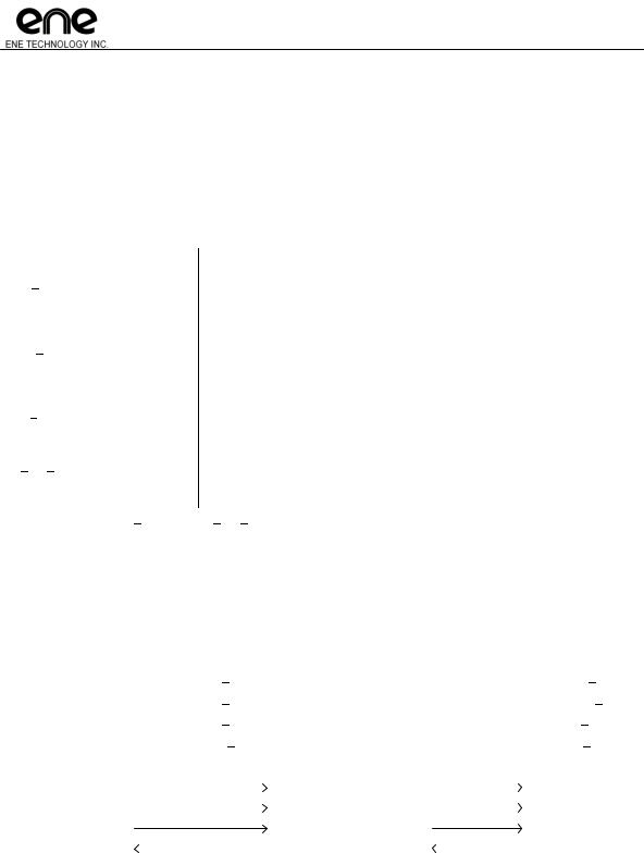
KB9012 Keyboard Controller Datasheet
3. Pin Descriptions
3.1 Hardware Trap
Hardware trap pins are used to latch external signal at rising edge of ECRST#. The hardware trap pins are for some special purpose which should be defined while boot-up. The following table gives the collection of hardware trap pins. Please note, all the following hardware trap pins are pull-high internally after reset.
Trap Name |
|
|
Pin No. |
|
|
Description |
|
|
|
|
|||||||
|
|
|
|
|
|
|
|
|
|
|
|
|
|
|
|
||
|
|
|
|
|
|
|
CONFIDENTIAL |
|
|||||||||
|
TP TEST |
|
|
|
39 |
|
|
While this trap is asserted to be low, the internal DPLL circuit uses other clock source |
|
||||||||
(GPIO20,KSO0) |
|
|
|
|
|
for reference, instead of 32KHz oscillator. |
|
|
|
|
|
||||||
|
|
|
|
|
|
|
|
|
|
|
Low: test clock mode enable |
|
|
|
|
|
|
|
|
|
|
|
|
|
|
|
|
|
High: normal mode using 32KHz oscillator. |
|
|
|
|
|
|
|
|
TP PLL |
|
|
|
40 |
|
|
While this trap is asserted to be low, some DPLL related signals can be output for |
|
|||||||
(GPIO21,KSO1) |
|
|
|
|
|
test. |
|
|
|
|
|
||||||
|
|
|
|
|
|
|
|
|
|
|
Low: DPLL test mode enable. |
|
|
|
|
|
|
|
|
|
|
|
|
|
|
|
|
|
High: DPLL test mode disable |
|
|
|
|
|
|
|
TP TMUX |
|
|
|
41 |
|
|
TestMux Mode Trap |
|
|
|
|
|
||||
(GPIO22,KSO2) |
|
|
|
|
|
Low: Test mode |
|
|
|
|
|
||||||
|
|
|
|
|
|
|
|
|
|
|
High: Normal operation |
|
|
|
|
|
|
|
TP |
|
PLL Lock |
|
|
42 |
|
|
This trap is used for eFlash & EDI operation, , the 8051 will be held at reset state |
|
|||||||
(GPIO23,KSO3) |
|
|
|
|
|
LOW: Test Mode |
|
|
|
|
|
||||||
|
|
|
|
|
|
|
|
|
|
|
HIGH: Normal operation |
|
|
|
|
|
|
|
|
Please note while TP TMUX and TP PLL Lock keep low at the same time, a mechanism called FlashDirectAccess will |
|
|
|||||||||||||
|
|
|
enable. That is, users can flush and program a SPI flash via specific IKB pins with external tool. |
|
|
|
|
||||||||||
FlashDirectAccess: |
|
|
|
|
|
|
|
|
|
|
|||||||
|
The KBC provides a new interface to program SPI flash via IKB interface. With this feature, users can easily utilize 4 pins |
|
|
||||||||||||||
from keyboard matrix (IKB) without disassembly whole machine. These 4 pins are connected directly to external SPI-Flash |
|
|
|||||||||||||||
interface. The following table shows the mapped pins while entering FlashDirectAccess mode. |
|
|
|
|
|||||||||||||
|
|
|
|
|
|
|
|
|
|
|
|
||||||
EDI : For detail ENE Debug Interface, please refer the EDI section for enabling, instruction, and application. |
|
|
|||||||||||||||
|
|
|
|
|
|
|
|
|
|
|
|
|
|
|
|||
|
Pin No. |
|
Normal Mode |
|
|
|
FlashDirectAccess Mode |
|
|
|
|
||||||
|
|
|
|
|
|
|
|
|
|
|
|
|
|
|
|
||
|
|
59 |
|
|
KSI4 (I) |
|
(Input) |
EDI CS, Transfer signal from terminal into KBC and though SPICS# to SPI Flash |
|
|
|||||||
|
|
|
|
|
|
|
|
|
|
|
|
|
|
|
|
||
|
|
60 |
|
|
KSI5 (I) |
|
(Input) |
EDI CLK, Transfer signal from terminal into KBC and though SPICLK to SPI Flash |
|
|
|||||||
|
|
|
|
|
|
|
|
|
|
|
|
|
|
|
|
||
|
|
61 |
|
|
KSI6 (I) |
|
(Input) |
EDI DIN, Transfer signal from terminal into KBC and though MOSI to SPI Flash |
|
|
|||||||
|
|
|
|
|
|
|
|
|
|
|
|
|
|
|
|||
|
|
62 |
|
|
KSI7 (I) |
|
(Output) EDI DO, Transfer signal from terminal into KBC and though MISO to SPI Flash |
|
|
||||||||
|
|
|
|
|
|
|
|
|
|
|
|
|
|
|
|
|
|
|
|
|
|
|
|
|
|
P59, KSI4 |
|
|
P128, SPICS# |
|
|
|
|
||
|
|
|
|
|
|
|
|
|
EDI_CS |
|
|
|
|
||||
|
|
|
|
|
|
|
|
|
|
|
|
|
|||||
|
|
|
|
|
|
|
|
|
|
|
|
|
|
|
|
|
|
|
|
|
|
|
|
|
|
P60, KSI5 |
|
EDI_CLKENE |
P126, SPICLK |
|
|
|
|
||
|
|
|
Terminal |
P61, KSI6 |
|
P120, MOSI |
SPI-Flash |
|
|
|
|||||||
|
|
|
|
EDI_DINKBC |
|
||||||||||||
|
|
|
|
|
|
|
|
P62, KSI7 |
|
P119, MISO |
|
|
|
|
|||
|
|
|
|
|
|
|
|
|
|
|
|
EDI_DO |
|
|
|
|
|
|
|
|
|
|
|
|
|
|
|
|
|
|
|
|
|
|
|
|
|
|
|
|
|
|
|
|
|
|
|
|
|
|
|
|
|
Copyright© 2011, ENE Technology Inc. |
15 |

KB9012 Keyboard Controller Datasheet
3.2Pin Descriptions by Functions
3.2.1Low Pin Count I/F Descriptions.
|
Pin Name |
|
Pin No. |
|
Direction |
|
|
|
Description |
|
|
|
|
|
|
|
|
|
|
|
|
|
|
|
LAD[3:0] |
5, 7,8,10 |
|
I/O |
|
|
|
LPC address bus. |
|
||
|
|
|
|
|
|
|
|
|
|
||
|
LFARAME# |
4 |
|
I |
|
|
|
LPC frame control signal. |
|
||
|
|
|
|
|
|
|
|
|
|
||
|
PCIRST# |
13 |
|
I |
|
|
|
LPC module reset by this signal. |
|
||
|
PCICLK |
12 |
|
I |
|
|
|
33MHz PCI clock input. |
|
||
|
SERIRQ |
3 |
|
I/O |
|
|
|
Serial IRQ |
|
||
|
|
CONFIDENTIAL |
|
||||||||
|
CLKRUN# |
38 |
|
I/OD |
|
|
|
Clock run control |
|
||
|
3.2.2 PS/2 I/F Descriptions |
|
|
|
|
|
|
||||
|
Pin Name |
|
Pin No. |
|
Direction |
|
|
|
Description |
|
|
|
PSCLK1 |
83 |
|
I/OD |
|
|
|
PS/2 port 1 clock |
|
||
|
|
|
|
|
|
|
|
|
Muxed with SMBus port 2 clock |
|
|
|
PSDAT1 |
84 |
|
I/OD |
|
|
|
PS/2 port 1 data |
|
||
|
|
|
|
|
|
|
|
|
Muxed with SMBus port 2 data |
|
|
|
PSCLK2 |
85 |
|
I/OD |
|
|
|
PS/2 port 2 clock |
|
||
|
|
|
|
|
|
|
|
|
Muxed with SMBus port 3 clock |
|
|
|
PSDAT2 |
86 |
|
I/OD |
|
|
|
PS/2 port 2 data |
|
||
|
|
|
|
|
|
|
|
|
Muxed with SMBus port 3 data |
|
|
|
PSCLK3 |
87 |
|
I/OD |
|
|
|
PS/2 port 3 clock |
|
||
|
PSDAT3 |
88 |
|
I/OD |
|
|
|
PS/2 port 3 data |
|
||
|
|
|
|
|
|
|
|
||||
|
3.2.3 Internal Keyboard Encoder (IKB) Descriptions |
||||||||||
|
|
|
|
|
|
|
|
|
|
||
|
Pin Name |
|
Pin No. |
|
Direction |
|
|
|
Description |
|
|
|
|
|
|
|
|
|
|
|
|
|
|
|
KSO[17:0] |
82,81,54-39 |
|
O |
|
|
|
Keyboard Scan Out |
|
||
|
KSI[7:0] |
62-55 |
|
I |
|
|
|
Keyboard Scan In |
|
||
|
3.2.4 SMBus Descriptions |
|
|
|
|
|
|
||||
|
|
|
|
|
|
|
|
|
|
||
|
Pin Name |
|
Pin No. |
|
Direction |
|
|
|
Description |
|
|
|
|
|
|
|
|
|
|
|
|
|
|
|
SCL0 |
77 |
|
I/OD |
|
|
|
SMBus clock (interface 0) |
|
||
|
SDA0 |
78 |
|
I/OD |
|
|
|
SMBus data (interface 0) |
|
||
|
|
|
|
|
|
|
|
|
|
||
|
SCL1 |
79 |
|
I/OD |
|
|
|
SMBus clock (interface 1) |
|
||
|
|
|
|
|
|
|
|
|
|
||
|
SDA1 |
80 |
|
I/OD |
|
|
|
SMBus data (interface 1) |
|
||
|
SCL2 |
83 |
|
I/OD |
|
|
|
SMBus clock (interface 2) |
|
||
|
|
|
|
|
|
|
|
|
Muxed with PS/2 port 1 clock |
|
|
|
|
|
|
|
|
|
|
|
|
||
|
SDA2 |
84 |
|
I/OD |
|
|
|
SMBus data (interface 2) |
|
||
|
|
|
|
|
|
|
|
|
Muxed with PS/2 port 1 data |
|
|
|
|
|
|
|
|
|
|
|
|
||
|
SCL3 |
85 |
|
I/OD |
|
|
|
SMBus clock (interface 3) |
|
||
|
|
|
|
|
|
|
|
|
Muxed with PS/2 port 2 clock |
|
|
|
|
|
|
|
|
|
|
|
|
||
|
SDA3 |
86 |
|
I/OD |
|
|
|
SMBus data (interface 3) |
|
||
|
|
|
|
|
|
|
|
|
Muxed with PS/2 port 2 data |
|
|
|
|
|
|
|
|
|
|
|
|
||
|
|
|
|
|
|
|
|
|
|
|
|
|
Copyright© 2011, ENE Technology Inc. |
|
|
16 |
|
|
|||||

|
|
|
|
|
KB9012 Keyboard Controller Datasheet |
||
|
3.2.5 FAN Descriptions |
|
|
|
|
||
|
|
|
|
|
|
|
|
|
Pin Name |
|
Pin No. |
Direction |
Description |
|
|
|
|
|
|
|
|
|
|
|
FANPWM0 |
26 |
O |
FANPWM0 output |
|
||
|
|
|
|
|
|
||
|
FANPWM1 |
27 |
O |
FANPWM1 output |
|
||
|
|
|
|
|
|
||
|
FANFB0 |
28 |
I |
FAN0 tachometer input |
|
||
|
FANFB1 |
29 |
I |
FAN1 tachometer input |
|
||
|
FANFB2 |
100 |
I |
FAN2 tachometer input |
|
||
|
FANFB3 |
101 |
I |
FAN3 tachometer input |
|
||
|
|
|
|
|
|
||
|
|
CONFIDENTIAL |
|||||
|
3.2.6 Pulse Width Modulation (PWM) Descriptions |
||||||
|
Pin Name |
|
Pin No. |
Direction |
Description |
|
|
|
PWM0 |
21 |
O |
PWM pulse output |
|
||
|
PWM1 |
23 |
O |
PWM pulse output |
|
||
|
PWM2 |
25 |
O |
PWM pulse output |
|
||
|
PWM3 |
34 |
O |
PWM pulse output |
|
||
|
3.2.7 Analog-to-Digital Converter Descriptions |
||||||
|
Pin Name |
|
Pin No. |
Direction |
Description |
|
|
|
AD[3:0] |
66-63 |
I |
10bit A/D converter input |
|
||
|
AD[5:4] |
76,75 |
I |
10bit A/D converter input |
|
||
|
AD6 |
73 |
I |
10bit A/D converter input |
|
||
|
|
|
|
|
|
||
|
AD7 |
74 |
I |
10bit A/D converter input |
|
||
|
|
|
|
|
|
||
|
3.2.8 Digital-to-Analog Converter Descriptions |
||||||
|
|
|
|
|
|
||
|
Pin Name |
|
Pin No. |
Direction |
Description |
|
|
|
|
|
|
|
|
|
|
|
DA[3:0] |
72-70,68 |
O |
8bit D/A converter output |
|
||
|
|
|
|
|
|
||
|
3.2.9 8051 External I/F Descriptions |
||||||
|
|
|
|
|
|
||
|
Pin Name |
|
Pin No. |
Direction |
Description |
|
|
|
|
|
|
|
|
|
|
|
E51TXD |
30 |
O |
8051 serial port, transmit port. |
|
||
|
|
|
|
|
|
||
|
E51RXD |
31 |
I |
8051 serial port, receive port. |
|
||
|
E51CLK |
31 |
O |
For different serial scheme, E51CLK will shift out clock. |
|
||
|
E51CS# |
90 |
O |
|
|
|
|
|
E51TMR0 |
92 |
I |
|
|
|
|
|
|
|
|
|
|
|
|
|
E51INT0 |
93 |
I |
|
|
|
|
|
|
|
|
|
|
|
|
|
E51TMR1 |
91 |
I |
|
|
|
|
|
E51INT1 |
95 |
I |
|
|
|
|
|
|
|
|
|
|
|
|
Copyright© 2011, ENE Technology Inc. |
17 |
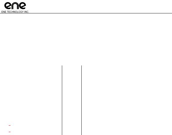
KB9012 Keyboard Controller Datasheet
3.2.10 External Clock Descriptions
(These pins are reserved for external CLK design structure, also could be set as GPIO function)
Pin Name |
|
Pin No. |
Direction |
Description |
|
|
|
|
|
XCLKI |
122 |
I |
32.768KHz input |
|
|
|
|
|
|
XCLKO |
123 |
O |
32.768KHz output |
|
|
|
|
|
|
3.2.11 Miscellaneous Signals Descriptions
Pin Name |
|
Pin No. |
|
Direction |
|
Description |
|
|
|
|
|
|
|
|
|
VCC |
|
CONFIDENTIAL9,22,33,96,111,125 Power supply for digital plane. |
|
||||
GA20 |
1 |
|
O |
|
KBC will gate A20 address line |
|
|
KBRST# |
2 |
|
O |
|
KBRST# is used to generate system reset. |
|
|
SCI# |
20 |
|
O |
|
SCI# asserts to the system for requesting service while |
|
|
|
|
|
|
|
|
related events occur. |
|
ECRST# |
37 |
|
I |
|
While ECRST# asserted, the KBC will reset globally. |
|
|
OWM |
16 |
|
I/O |
|
One Wire Master input and output signal |
|
|
PECI |
118 |
|
I/O |
|
PECI input and output signal |
|
|
GWG |
108 |
|
O |
|
General Waveform Generator for 3D application |
|
|
POWER FAIL0 |
100 |
|
O |
|
Used to indicate the power fail under Power Fail Voltage. |
|
|
POWER FAIL1 |
32 |
|
O |
|
Used to indicate the power fail under Power Fail Voltage. |
|
|
3.2.12 Voltage Comparator Pins Descriptions |
|||||||
|
|
|
|
|
|
|
|
Pin Name |
|
Pin No. |
|
Direction |
|
Description |
|
|
|
|
|
|
|
|
|
VCIN0 |
109 |
|
I |
|
Voltage comparator input port0 |
|
|
|
|
|
|
|
|
|
|
VCOUT0 |
104 |
|
O |
|
Voltage comparator output port0 |
|
|
|
|
|
|
|
|
|
|
VCIN1 |
102 |
|
I |
|
Voltage comparator input port1 |
|
|
VCOUT1 |
103 |
|
O |
|
Voltage comparator output port1 |
|
|
|
|
|
|
|
|
|
|
3.2.13 Power Pins Descriptions |
|
|
|
||||
|
|
|
|
|
|
|
|
Pin Name |
|
Pin No. |
|
Direction |
|
Description |
|
|
|
|
|
|
|
|
|
|
|
|
|
|
|
|
|
GND |
11,24,35,94,113 |
|
|
|
Power ground for digital plane. |
|
|
AVCC |
67 |
|
|
|
Power supply for analog plane. |
|
|
|
|
|
|
|
|
|
|
AGND |
69 |
|
|
|
Power ground for analog plane. |
|
|
|
|
|
|
|
|
|
|
V18R |
124 |
|
|
|
Connected to external Capacitor for internal 1.8V |
|
|
VCC_0 |
111 |
|
|
|
Power supply for 51ON power management |
|
|
GND_0 |
113 |
|
|
|
Power ground for 51ON power management |
|
|
|
|
|
|
|
|
|
|
Copyright© 2011, ENE Technology Inc. |
18 |

KB9012 Keyboard Controller Datasheet
3.2.14 51ON Power Pins Descriptions
(The 51ON power management are with different power domain from main IC power)
Pin Name |
|
Pin No. |
Direction |
Description |
|
|
|
|
|
|
|
GPXIOD01 |
110 |
I/O |
AC_IN |
|
|
|
|
|
|
|
|
GPXIOD02 |
112 |
I/O |
ALW_PWR_EN |
|
|
|
|
|
|
|
|
GPXIOD03 |
114 |
I/O |
ON/OFFBTN# |
|
|
|
|
|
|
|
|
CONFIDENTIAL |
|||||
Copyright© 2011, ENE Technology Inc. |
19 |

KB9012 Keyboard Controller Datasheet
4.Module Descriptions
4.1 Chip Architecture
4.1.1 Power Planes
Power planes are ±10% tolerance for recommend operation condition, The KBC |
provides |
|||||
V1.8 power plane for different generation. |
|
|
|
|
||
|
|
|
|
|
|
|
Power Plane |
|
Description |
Power |
|
Ground |
|
|
|
|
|
|
|
|
Digital Plane |
|
This power provides power for all digital logic no matter what |
VCC |
|
GND |
|
|
|
power mode is. |
|
|
|
|
|
|
|
|
|
|
|
|
|
|
|
|
||
|
CONFIDENTIAL |
|
|
|
||
Analog Plane |
|
This power provides power for all analog logic, such as A/D |
AVCC |
|
AGND |
|
|
|
and D/A converter. |
|
|
|
|
Digital V1.8 |
|
The system inputs 3.3V power and the internal regulator |
V1.8 |
|
GND |
|
|
|
outputs 1.8V voltage. The 1.8V output should connect a |
|
|
|
|
|
|
capacitor for stable purpose. |
|
|
|
|
Power Latch |
|
This power provides power for the power-latch circuit. It could |
VCC 0 |
|
GND 0 |
|
Plane |
|
help to provide power saving management. |
|
|
|
|
Copyright© 2011, ENE Technology Inc. |
20 |
Loading...