

Ene KB3930QF Schematics

KB3930 for OLPC
Keyboard Controller
Data Sheet
V 0.2
May. 2010
ENE RESERVES THE RIGHT TO AMEND THIS DOCUMENT WITHOUT NOTICE AT ANY TIME. ENE
ASSUMES NO RESPONSIBILITY FOR ANY ERRORS APPEAR IN THE DOCUMENT, AND ENE DISCLAIMS
ANY EXPRESS OR IMPLIED WARRANTY, RELATING TO SALE AND/OR USE OF ENE PRODUCTS
INCLUDING LIABILITY OR WARRANTIES RELATING TO FITNESS FOR A PARTICULAR PURPOSE, OR
INFRINGEMENT OF ANY PATENTS, COPYRIGHTS OR OTHER INTELLECTUAL PROPERTY RIGHTS.
Headquarters
4F-1, No.9, Prosperity Rd.,
Science-based Industrial Park,
Hsinchu City, Taiwan, R.O.C
TEL: 886-3-6662888
FAX: 886-3-6662999
http://www.ene.com.tw
Copyright©2010, ENE Technology Inc. All rights reserved.
Taipei Office
4F, No.88, Bauchiau Rd.
Shindian City, Taipei,
Taiwan, R.O.C.
TEL: 886-2-89111525
FAX: 886-2-89111523

t
KB3930 Keyboard Controller Datasheet
Revision
Revision Description Date
0.1 1. 1
0.2 1. Remove Watermark 2010/5
s
release as KB3930 OLPC datasheet 2010/04 (0.7)
Copyright©2010, ENE Technology Inc.
i

KB3930 Keyboard Controller Datasheet
1. GENERAL DESCRIPTION .................................................................................. 0
1.1 OVERVIEW ........................................................................................................ 0
1.2 FEATURES ........................................................................................................ 1
1.3 COMPARISON (KB3926D VS. KB3930).............................................................. 6
1.4 BLOCK DIAGRAM .............................................................................................. 7
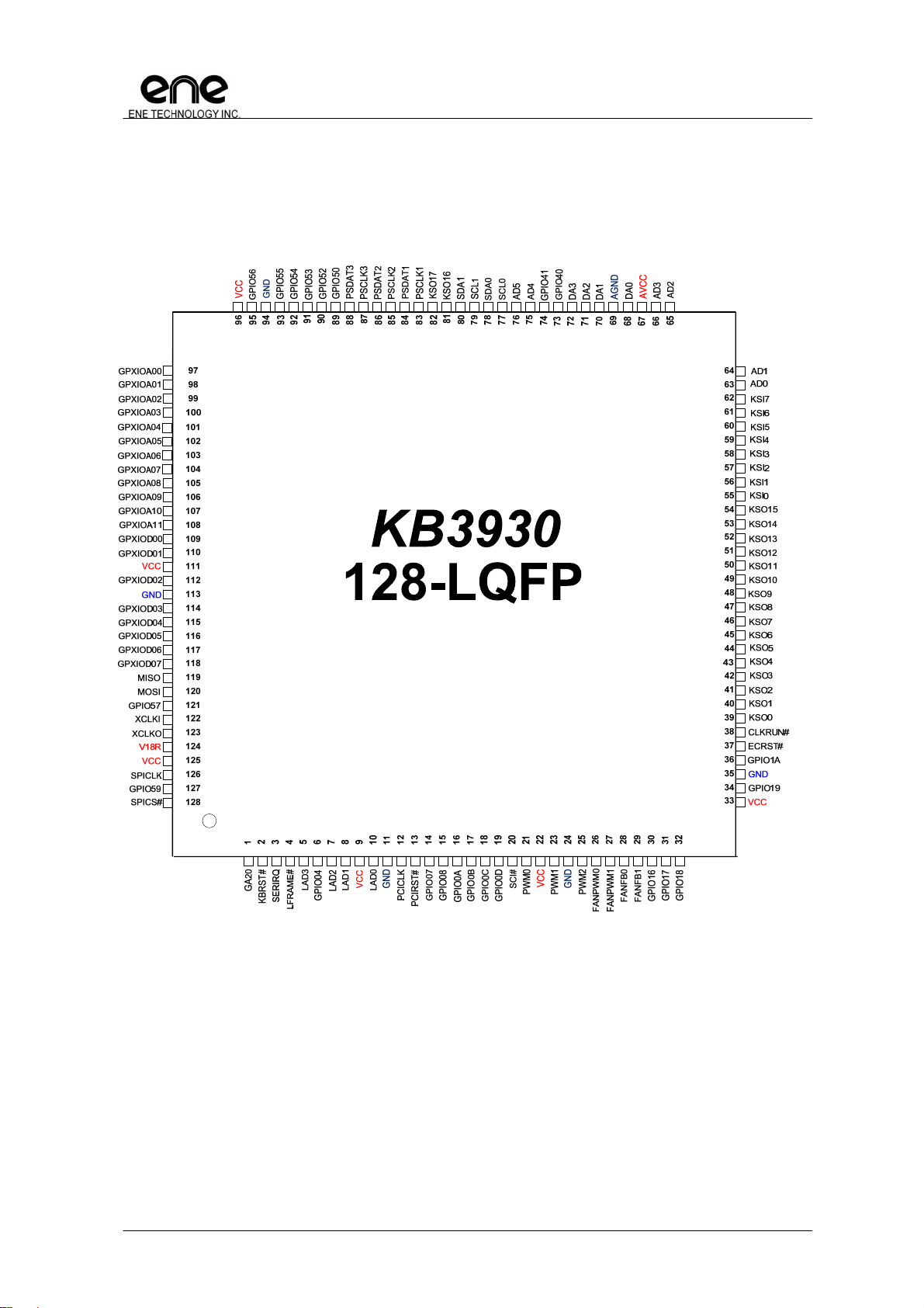
2. PIN ASSIGNMENT AND DESCRIPTION ............................................................ 8
2.1 KB3930 128-PIN LQFP DIAGRAM TOP VIEW ..................................................... 8
2.2 KB3930 128 LFBGA BALL MAP ...................................................................... 9
KB3930 PIN ASSIGNMENT SIDE A ................................................................... 10
2.3
2.4 KB3930 PIN ASSIGNMENT SIDE B ................................................................... 11
2.5
KB3930 PIN ASSIGNMENT SIDE C ................................................................... 12
2.6 KB3930 PIN ASSIGNMENT SIDE D ................................................................... 13
2.7 I/O CELL DESCRIPTIONS .................................................................................. 14
2.7.1 I/O Buffer Table ..................................................................................... 14
2.7.2 I/O Buffer Characteristic Table ............................................................ 14
3. PIN DESCRIPTIONS ......................................................................................... 15
3.1 HARDWARE TRAP ........................................................................................... 15
3.2 PIN DESCRIPTIONS BY FUNCTIONS ................................................................... 16
3.2.1 Low Pin Count I/F Descriptions. ......................................................... 16
3.2.2 SPI Flash I/F Descriptions ................................................................... 16
3.2.3 PS/2 I/F Descriptions ............................................................................ 16
3.2.4 Internal Keyboard Encoder (IKB) Descriptions ................................. 17
3.2.5 SMBus Descriptions ............................................................................ 17
3.2.6 FAN Descriptions ................................................................................. 17
3.2.7 Pulse Width Modulation (PWM) Descriptions .................................... 17
3.2.8 Analog-to-Digital Converter Descriptions .......................................... 17
3.2.9 Digital-to-Analog Converter Descriptions .......................................... 18
3.2.10 8051 External I/F Descriptions .......................................................... 18
3.2.11 External Clock Descriptions .............................................................. 18
3.2.12 Miscellaneous Signals Descriptions ................................................ 18
3.2.13 Voltage Comparator Pins Descriptions ............................................ 19
3.2.14 Power Pins Descriptions ................................................................... 19
4. MODULE DESCRIPTIONS ................................................................................ 20
4.1 CHIP ARCHITECTURE ....................................................................................... 20
4.1.1 Power Planes ........................................................................................ 20
4.1.2 Clock Domains ..................................................................................... 21
Copyright©2010, ENE Technology Inc.
ii

KB3930 Keyboard Controller Datasheet
4.1.4 Internal Memory Map ........................................................................... 24
4.2 GPIO ............................................................................................................. 25
4.2.1 GPIO Function Description ................................................................. 25
4.2.2 GPIO Structures ................................................................................... 28
4.2.3 GPIO Attribution Table ......................................................................... 29
4.2.3 GPIO Registers Descriptions .............................................................. 32
4.2.4 GPIO Programming Sample ................................................................ 43
4.3 KEYBOARD AND MOUSE CONTROL INTERFACE (KBC) ....................................... 44
4.3.1 KBC I/F Function Description ............................................................. 44
ENE SERIAL BUS CONTROLLER (ESB) ............................................................ 49
4.4
4.4.1 ESB Function Description ................................................................... 49
4.4.2 ESB Registers Description .................................................................. 50
4.5
RESERVED ...................................................................................................... 56
4.6 PECI ............................................................................................................. 57
4.6.1 PECI Functional Description ............................................................... 57
4.6.2 PECI Register Description (Base address = FCD0h, 16 bytes) ........ 58
4.7 OWM ............................................................................................................ 61
4.7.1 OWM Functional Description .............................................................. 61
4.8 PULSE WIDTH MODULATION (PWM) ................................................................. 65
4.8.1 PWM Function Description .................................................................. 65
4.8.2 PWM Registers Description ................................................................ 66
4.8.3 PWM Programming Sample ................................................................ 68
FAN CONTROLLER ........................................................................................... 69
4.9
4.9.1 Fan Function Description .................................................................... 69
4.9.2 Fan Registers Description ................................................................... 70
4.9.3 Fan Programming Sample ................................................................... 76
4.10
GENERAL PURPOSE TIMER (GPT) .................................................................. 77
4.10.1 GPT Function Description ................................................................. 77
4.10.2 GPT Registers Description ................................................................ 77
4.10.3 GPT Programming Sample ................................................................ 79
4.11 SDI HOST/DEVICE INTERFACE CONTROLLER ................................................... 80
4.11.1 SDI Host/Device Interface Description ............................................. 80
4.11.2 SDI Host Interface Description .......................................................... 80
4.11.2 SDI Device Interface Description ...................................................... 81
4.11.3 SDI Programming Sample ................................................................. 84
4.12 WATCHDOG TIMER (WDT) ............................................................................. 85
Copyright©2010, ENE Technology Inc.
iii

KB3930 Keyboard Controller Datasheet
4.12.1 WDT Function Description ................................................................ 85
4.12.2 WDT Registers Description ............................................................... 85
4.12.3 WDT Programming Sample ............................................................... 88
4.13 LOW PIN COUNT INTERFACE (LPC) ................................................................ 89
4.13.1 LPC Function Description ................................................................. 89
4.13.2 LPC I/O Decode Range ...................................................................... 89
4.13.3 LPC Memory Decode Range ............................................................. 89
4.13.4 FWH Memory Decode Range ............................................................ 90
4.13.5 Index-I/O Port ...................................................................................... 90
4.13.6 Extended I/O Port (Debug Port, Port80) ........................................... 91
4.13.7 LPC Registers Description ................................................................ 92
X-BUS INTERFACE (XBI) ............................................................................. 100
4.14
4.14.1 XBI Function Description ................................................................ 100
4.14.2 XBI SPI Enhancement ...................................................................... 100
4.14.3 XBI Registers Description ............................................................... 103
4.15
CONSUMER IR CONTROLLER (CIR) .............................................................. 109
4.15.1 CIR Function Description ................................................................ 109
4.15.2 CIR Block Diagram ........................................................................... 111
4.15.3 CIR Remote Protocol ....................................................................... 112
4.15.3.1 Philips RC5 Protocol ............................................................................................ 11 2
4.15.3.2 Philips RC6 Protocol ............................................................................................ 11 3
4.15.3.3 NEC Protocol ........................................................................................................ 11 3
4.15.4 CIR Automatic Carrier Frequency Detection and Modulation ...... 114
4.15.5 CIR Registers Description ............................................................... 116
4.15.3 CIR Programming Sample ............................................................... 120
PS/2 INTERFACE (PS/2) .............................................................................. 121
4.16
4.17
EMBEDDED CONTROLLER (EC) .................................................................... 122
4.17.1 EC Function Description ................................................................. 122
4.17.2 EC Command Program Sequence .................................................. 123
4.17.3 EC SCI Generation ........................................................................... 124
4.17.4 EC/KBC Clock Configuration .......................................................... 125
4.17.5 A/D Converter Control ...................................................................... 125
4.17.6 D/A Converter Control ...................................................................... 127
4.17.7 Power Management Control ............................................................ 128
4.17.8 EC Registers Description ................................................................ 129
4.18 GENERAL PURPOSE WAKE-UP CONTROLLER (GPWU) .................................. 140
4.18.1 GPWU Function Description ........................................................... 140
Copyright©2010, ENE Technology Inc.
iv

KB3930 Keyboard Controller Datasheet
4.18.2 GPWU Registers Description .......................................................... 141
4.18.3 GPWU Programming Sample .......................................................... 146
4.19 SYSTEM MANAGEMENT BUS CONTROLLER (SMBUS) .................................... 147
4.19.1 SMBus Function Description .......................................................... 147
4.19.2 SMBus Register Description ........................................................... 149
4.20 8051 MICROPROCESSOR ............................................................................. 154
4.20.1 8051 Microprocessor Function Description ................................... 154
4.20.2 8051 Microprocessor Instruction .................................................... 155
4.20.3 8051 Interrupt Controller ................................................................. 159
4.20.4 Interrupt Enable/Flag Table ............................................................. 160
4.20.5 8051 Special Function Register (SFR) ............................................ 162
4.20.6 8051 Microprocessor Register Description ................................... 163
5. ELECTRICAL CHARACTERISTICS ............................................................... 170
5.1 ABSOLUTE MAXIMUM RATI NG ........................................................................ 170
5.2 DC ELECTRICAL CHARACTERISTICS ............................................................... 170
BQCZ16HIV .................................................................................................. 170
BQC04HIV .................................................................................................... 170
BQCW16HIV ................................................................................................. 171
BCC16HI ....................................................................................................... 171
BQC04HI ....................................................................................................... 172
IQTHI (ADC cell) .......................................................................................... 172
OCT04H (DAC cell) ...................................................................................... 172
BQC08HIV .................................................................................................... 173
BQC04HIVPECI ............................................................................................ 173
A/D & D/A CHARACTERISTICS ....................................................................... 174
5.3
5.5 OPERATING CURRENT ................................................................................... 175
5.6
PACKAGE THERMAL INFORMATION.................................................................. 175
5.7 AC ELECTRICAL CHARACTERISTICS ............................................................... 176
5.7.1 SPI Flash Timing ................................................................................ 176
5.7.2 LPC interface Timing ......................................................................... 177
5.7.3 PS/2 interface Timing ......................................................................... 179
5.7.4 SMBus interface Timing .................................................................... 180
2. SMBUS frequencry dependant ........................................................... 180
5.7.5 PECI interface Timing ........................................................................ 181
5.7.6 OWM interface Timing ....................................................................... 182
6. PACKAGE INFORMATION ............................................................................. 183
Copyright©2010, ENE Technology Inc.
v

KB3930 Keyboard Controller Datasheet
6.1 LQFP 128-PIN OUTLINE DIAGRAM ................................................................ 183
6.1.1 Top View .............................................................................................. 183
6.1.2 Side View ............................................................................................ 184
6.1.3 Lead View ............................................................................................ 185
6.1.4 LQFP Outline Dimensions ................................................................. 186
6.2 LFBGA 128-PIN OUTLINE DIAGRAM .............................................................. 187
6.2.1 Top View .............................................................................................. 187
6.2.2 Side View ............................................................................................ 188
6.2.3 Bottom View........................................................................................ 189
6.2.4 LFBGA Outline Dimensions .............................................................. 190
PART NUMBER DESCRIPTION ......................................................................... 191
6.3
Copyright©2010, ENE Technology Inc.
vi

1. General Description
1.1 Overview
The ENE KB3930 is a highly customized embedded controller (EC) for notebook platforms.
The embedded controller contains industrial standard 8051 microprocessor and provides function of
i8042 keyboard controller basically. KB3930 is embedded LPC interface used to communicate with
Host. KB3930 is designed with Shared-ROM architecture. The EC firmware and system BIOS will
co-exist in single SPI flash. The embedded controller also features rich interfaces for general
applications, such as PS/2 interface, Keyboard matrix encoder, PWM controller, A/D converter, D/A
converter, Fan controller, SMBus controller, GPIO controller, PECI controller, one wire master, SPI
controller, voltage comparator and extended interface (ENE Serial Bus) for more applications, like
capacitive touch button application and GPIO extender.
Compared with last generation of KB3926 series, KB3930 added PECI/OWM, another 2
SMBus, another 2 Fan tachometers, enhanced SPI host/slave controller, voltage comparator,
internal oscillator for newest application. KB3930 also improves structure of other modules including
8051, XBI, LPC, IKB, FAN, WDT, GPIO, ESB, EDI. For detail improvement, please refer the related
section.
1.2 Features
LPC Low Pin Count Interface
SIRQ supporting IRQ1, IRQ12, SCI or SMI# interrupt and one programmable
I/O Address Decoding:
Memory Decoding:
Compatible with LPC specification v1.1
Support LPC interface re-direction to IKB for debugging
KB3930 Keyboard Controller Datasheet
IRQ provided.
Legacy KBC I/O port 60h/64h
Programmable EC I/O port, 62h/66h(recommend)
I/O port 68h/6Ch (sideband)
2 Programmable 4-byte Index-I/O ports to access internal EC registers.
1 Programmable extended (debug) port I/O.
Firmware Hub decode
LPC memory decode
X-bus Bus Interface (XBI) : Flash Interface
SPI flash is supported, size up to 4MB.
SPI frequency supports 33/45/66MHz.
New SPI command (dual read) to enhance the performance.
The 64KB code memory can be mapped into system memory by one 16KB and
one 48KB programmable pages independently.
Support SPI flash in-system-programming via IKB pins.
Enhanced pre-fetch mechanism.
8051 Microprocessor
Compatible with industrial 8051 instructions with 3 cycles.
8051 runs at 8/16/22 MHz, programmable.
256 bytes internal RAM and 4KB tight-coupled SRAM.
24 extended interrupt sources.
Two 16-bit timers.
Full duplex UART integrated.
Supports idle and stop mode.
Enhanced ENE debug interface.
Support Tx/Rx re-direction to IKB for debugging
Copyright©2010, ENE Technology Inc.
1
8042 Keyboard Controller
8 standard 8042 commands processed by hardware.
Each hardware command can be optionally processed by firmware.
Pointing device multiplex mode support.
Fast GA20 and KB reset support.
PS/2 Controller
Support at most 3 external PS/2 devices.
External PS/2 device operation in firmware mode.
Internal Keyboard Matrix (IKB)
18x8 keyboard scan matrix.
Support W2K Internet and multimedia keys.
Support hotkey events defined.
Ghost key cancellation mechanism provided.
KB3930 Keyboard Controller Datasheet
Enhanced de-bounce feature added
Embedded Controller (EC)
ACPI Spec 2.0 compliant.
5 standard EC command supported directly by hardware.
Each hardware command can be processed by firmware optionally.
Programmable EC I/O ports, 62h/66h by default.
SMBus Host Controller
4 SMBus interfaces with 2 SMBus controllers
SMBus Spec 2.0 compliant.
Byte mode support.
Slave function support.
Digital-to-Analog Converter (DAC)
4 DAC channels with 8-bit resolution.
All DAC pins can be alternatively configured as GPO (general purpose output)
function.
Copyright©2010, ENE Technology Inc.
2
Analog-to-Digital Converter (ADC)
6 ADC channels with 10-bit resolution.
All ADC pins can be alternatively configured as GPI (general purpose input)
function.
Pulse Width Modulator (PWM)
6 PWM channels are provided. (8-bit *2, 14-bit *2 and FANPWM(12-bit) *2)
Clock source selectable:.
1MHz/64KHz/4KHz/256Hz (for 8-bit PWM)
Peripheral clock or 1MHz (for 14-bit PWM)
Peripheral clock (for FANPWM)
Duty cycle programmable and cycle time up to 1 sec(for 8-bit PWM)
Watch Dog Timer (WDT)
32.768KHz input clock.
KB3930 Keyboard Controller Datasheet
10-bit counter with 32ms unit for watchdog reset.
Three watchdog reset mechanisms.
Reset 8051 only
Reset whole chip, except GPIO module.
Reset whole chip including GPIO module.
Real Time Clock
32.768KHz input clock.
24-bit timer support.
General Purpose Timer (GPT)
Two 16-bit and two 8-bit general purpose timer with 32.768KHz clock source.
General Purpose Wakeup (GPWU)
Those I/O with GPI (general purpose input) configuration can generate
interrupts or wakeup events, except those pins named in GPXIOAxx.
Copyright©2010, ENE Technology Inc.
3
General Purpose Input/Output (GPIO)
All general purpose I/O can be programmed as input or output.
All output pins can be configured to be tri-state optionally.
All input pins are equipped with pull-up, high/low active and edge/level trigger
selection.
For the pins of DAC can be configured as GPO function only.
For the pins of ADC can be configured as GPI function only.
A specific pair of GPIO pins with signal pass-through feature.
FAN Controller
Two fan controllers with tachometer inputs.
Automatic fan control support.
12-bit FANPWM support.
Enhanced FAN tracking resolution added
KB3930 Keyboard Controller Datasheet
Consumer IR (CIR)
Several protocols decoded/encoded by hardware.
Interrupt for CIR application.
Support wide/narrow band receiver.
Transmit/Receive simultaneously.
Remote power-on support.
ENE Serial Bus Interface (ESB)
A proprietary and flexible interface for extension with ENE KBC.
Firmware accesses ESB devices via internal memory address directly.
Interrupt capability.
ENE Debug Interface (EDI)
Flexible debug interface with SPI pins.
Keil-C development tool compatible
SPI Device Interface (SDI)
An enhanced SPI host/device controller is embedded.
Flexible design for SPI applications.
Copyright©2010, ENE Technology Inc.
4

One Wire Master Interface
Embedded One Wire controller used to control one wire devices.
KB3930 Keyboard Controller Datasheet
PECI
Support Intel PECI
Support wide speed range from 2Kbps to 2Mbps.
Power Management
Sleep mode: 8051 program counter (PC) stops and enters idle mode.
Deep sleep mode: All clocks stop except external 32.768KHz OSC. 8051 enters
stop mode.
Misc.
Support two hardware voltage comparator (initialed by F/W, operated by H/W),
two voltage input sources and one digital output, used to detect abnormal
situation (like over temperature).
Support two output pins to report KB3930 power fail status.
Package
128-pin LQFP package, Lead Free (RoHS).
Copyright©2010, ENE Technology Inc.
5
KB3930 Keyboard Controller Datasheet
1.3 Comparison (KB3926D vs. KB3930)
Microprocessor 8051 8051
Built-in SRAM 2KB 4KB
LPC 2 index-I/O sets 2 index I/O sets
X-Bus SPI ROM: 4MB
Enhanced pre-fetch mechanism.
Real Time Clock Support Support
ADC Six 10-bit ADC channels Six 10-bit ADC channels
DAC Four 8-bit DAC channels Four 8-bit DAC channels
WDT 128ms timer unit with 8bits control 32ms timer unit with 10bits control
PWM 6 sets
PWM0/1 – 8 bit
PWM2/3 – 14 bit
FANPWM0/1 – 12 bit
External PS/2 I/F 3 3
GPIO Programmable Bi-direction I/O
GPIO pass through : 1 pair
Max GPIO: 100
IKB Matrix 18x8 18x8
FAN controller 2 2 (Enhanced precision and 2
GPT 4 4
SMBus 2
Byte mode support
CIR Hardware encode/decode
IRQ and I/O port support
Carrier frequency calculation
TX with carrier modulation
Learning mode support
TX/RX simultaneously
EDI Enhanced Enhanced (Support break point)
ESB Support Support
SDI Support Support both SPI host/device
Package 128 LQFP 128 LQFP
Dimension 14mmx14mm 14mm x 14 mm
New-added
PECI
Function
KB3926D KB3930
SPI ROM: 4MB
Enhanced pre-fetch mechanism.
6 sets
PWM0/1 – 8 bit
PWM2/3 – 14 bit
FANPWM0/1 – 12 bit
Enhanced Bi-direction I/O cell
GPIO pass through : 1 pair
Max GPIO: 100
additional Tachometer Monitors)
4
Byte mode support
Hardware encode/decode
IRQ and I/O port support
Carrier frequency calculation
TX with carrier modulation
Learning mode support
TX/RX simultaneously
One Wire Master
POFR signals
Voltage Comparator
Copyright©2010, ENE Technology Inc.
6

1.4 Block Diagram
KB3930 Keyboard Controller Datasheet
Copyright©2010, ENE Technology Inc.
7
2. Pin Assignment and Description
2.1 KB3930 128-pin LQFP Diagram Top View
KB3930 Keyboard Controller Datasheet
Copyright©2010, ENE Technology Inc.
8

KB3930 Keyboard Controller Datasheet
2.2 KB3930 128 LFBGA Ball Map
This page is leaved blank intentionally.
Copyright©2010, ENE Technology Inc.
9

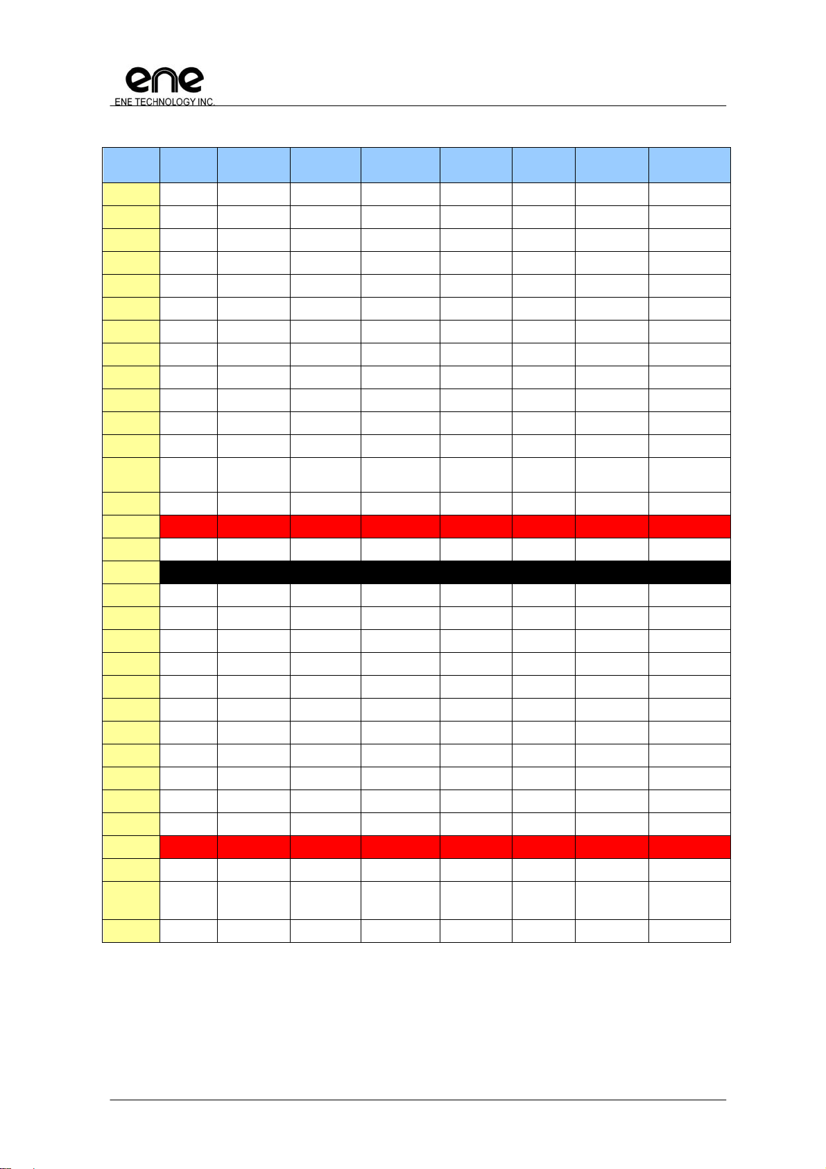
2.3 KB3930 Pin Assignment Side A
KB3930
Pin No.
10
11
12
13
14
15
16
17
18
19
20
21
22
23
24
25
26
27
28
29
30
31
32
KB3930
BGA
1
2
3
4
5
6
7
8
9
Name GPIO Alt
GA20 GPIO00 GA20 GPIO00 HiZ / HiZ BQC04HIV
KBRST# GPIO01 KBRST# GPIO01 HiZ / HiZ BQC04HIV
SERIRQ HiZ / HiZ BCC16HI
LFRAME# HiZ / HiZ BCC16HI
LAD3 HiZ / HiZ BCC16HI
GPIO04 GPIO04 GPIO04 HiZ / HiZ BQC04HIV
LAD2 HiZ / HiZ BCC16HI
LAD1 HiZ / HiZ BCC16HI
VCC VCC
LAD0 HiZ / HiZ BCC16HI
GND GND
PCICLK IE/IE BCC16HI
PCIRST# GPIO05 PCIRST# GPIO05 HiZ / IE BCC16HI
GPIO07 GPIO07 i_clk_8051 GPIO07 HiZ / HiZ BQC04HIV
GPIO08 GPIO08 i_clk_peri GPIO08 HiZ / HiZ BQC04HIV
GPIO0A GPIO0A OWM RLC_RX2
GPIO0B GPIO0B ESB_CLK GPIO0B PU / PU BQCW16HIV
GPIO0C GPIO0C ESB_DAT ESB_DAT GPIO0C HiZ / HiZ BQC08HIV
GPIO0D GPIO0D RLC_TX2 GPIO0D HiZ / HiZ BQC04HIV
SCI# GPIO0E SCI# GPIO0E HiZ / HiZ BQC04HIV
PWM0 GPIO0F PWM0 GPIO0F HiZ / HiZ BQC16HIV
VCC VCC VCC
PWM1 GPIO10 PWM1 GPIO10 HiZ / HiZ BQC04HIV
GND GND GND
GPIO11 GPIO11 PWM2 GPIO11 HiZ / HiZ BQC04HIV
FANPWM0 GPIO12 FANPWM0 GPIO12 HiZ / HiZ BQC04HIV
FANPWM1 GPIO13 FANPWM1 GPIO13 HiZ / HiZ BQC04HIV
FANFB0 GPIO14 FANFB0 GPIO14 HiZ / HiZ BQC04HIV
FANFB1 GPIO15 FANFB1 GPIO15 HiZ / HiZ BQC04HIV
GPIO16 GPIO16 E51TXD GPIO16 HiZ / HiZ BQC04HIV
GPIO17 GPIO17 E51CLK E51RXD GPIO17 HiZ / HiZ BQC04HIV
GPIO18 GPIO18 GPIO18 HiZ / HiZ BQC04HIV
Output
KB3930 Keyboard Controller Datasheet
Alt.
Input
OWM
Default ECRST#
L/H
GPIO0A HiZ / HiZ BQC04HIV
IO CELL
Copyright©2010, ENE Technology Inc.
10
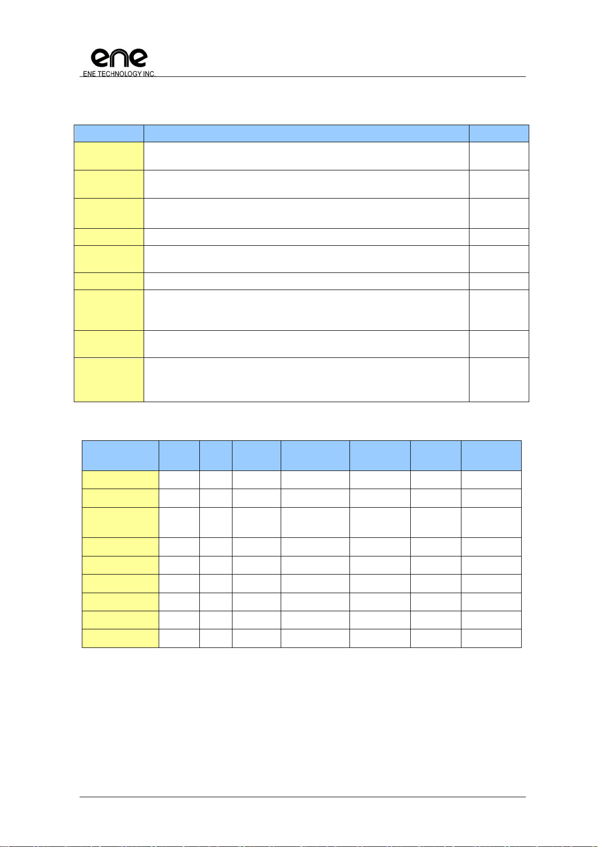
2.4 KB3930 Pin Assignment Side B
KB3930
Pin No.
33
34
35
36
37
38
39
40
41
42
43
44
45
46
47
48
49
50
51
52
53
54
55
56
57
58
59
60
61
62
63
64
KB3930
BGA
Name GPIO Alt
VCC VCC
GPIO19 GPIO19 PWM3 GPIO19 HiZ / HiZ BCC16HI
GND GND
GPIO1A GPIO1A NUMLED# GPIO1A HiZ / HiZ BCC16HI
ECRST# IE / IE BQC04HIV
CLKRUN# GPIO1D CLKRUN# CLKRUN# GPIO1D HiZ / HiZ BCC16HI
KSO0 GPIO20 KSO0 TP_TEST GPIO20 IE(PU)/IE(PU) BQC04HIV
KSO1 GPIO21 KSO1 TP_PLL GPIO21 IE(PU)/IE(PU) BQC04HIV
KSO2 GPIO22 KSO2 TP_TMUX GPIO22 IE(PU)/IE(PU) BQC04HIV
KSO3 GPIO23 KSO3 TP_ISP GPIO23 IE(PU)/IE(PU) BQC04HIV
KSO4 GPIO24 KSO4 GPIO24 HiZ / HiZ BQC04HIV
KSO5 GPIO25 KSO5 PCICLK
KSO6 GPIO26 KSO6 PCIRST#
KSO7 GPIO27 KSO7
SERIRQ(LPC) SERIRQ(LPC)
KSO8 GPIO28 KSO8 LFRAME#
KSO9 GPIO29 KSO9 GPIO29 HiZ / HiZ BQCZ16HIV
KSO10 GPIO2A KSO10 GPIO2A HiZ / HiZ BQCZ16HIV
KSO11 GPIO2B KSO11
KSO12 GPIO2C KSO12
KSO13 GPIO2D KSO13
KSO14 GPIO2E KSO14
KSO15 GPIO2F KSO15 E51_RXD GPIO2F HiZ / HiZ BQC04HIV
KSI0 GPIO30 E51_TXD KSI0 GPIO30 IE(PU)/IE(PU) BQC04HIV
KSI1 GPIO31 KSI1 GPIO31 IE(PU)/IE(PU) BQC04HIV
KSI2 GPIO32 KSI2 GPIO32 IE(PU)/IE(PU) BQC04HIV
KSI3 GPIO33 KSI3 GPIO33 IE(PU)/IE(PU) BQC04HIV
KSI4 GPIO34 KSI4/EDI_CS GPIO34 IE(PU)/IE(PU) BQC04HIV
KSI5 GPIO35 KSI5/EDI_CLK GPIO35 IE(PU)/IE(PU) BQC04HIV
KSI6 GPIO36 KSI6/EDI_DIN GPIO36 IE(PU)/IE(PU) BQC04HIV
KSI7 GPIO37 EDI_DO KSI7 GPIO37 IE(PU)/IE(PU) BQC04HIV
AD0 GPI38 AD0 GPI38 HiZ / HiZ IQTHI
AD1 GPI39 AD1 GPI39 HiZ / HiZ IQTHI
Output
LAD3(LPC)
LAD2(LPC)
LAD1(LPC)
LAD0(LPC)
KB3930 Keyboard Controller Datasheet
Alt.
Input
(LPC)
(LPC)
(LPC)
LAD3(LPC)
LAD2(LPC)
LAD1(LPC)
LAD0(LPC)
Default ECRST#
L/H
GPIO25 HiZ / HiZ BQCZ16HIV
GPIO26 HiZ / HiZ BQC04HIV
GPIO27 HiZ / HiZ BQC04HIV
GPIO28 HiZ / HiZ BQC04HIV
GPIO2B HiZ / HiZ BQC04HIV
GPIO2C HiZ / HiZ BQC04HIV
GPIO2D HiZ / HiZ BQC04HIV
GPIO2E HiZ / HiZ BQC04HIV
IO CELL
Copyright©2010, ENE Technology Inc.
11
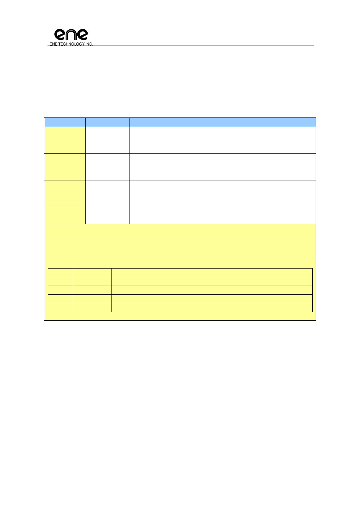
2.5 KB3930 Pin Assignment Side C
KB3930
Pin No.
65
66
67
68
69
70
71
72
73
74
75
76
77
78
79
80
81
82
83
84
85
86
87
88
89
90
91
92
93
94
95
96
KB3930
BGA
Name GPIO Alt
AD2 GPI3A AD2 GPI3A HiZ / HiZ IQTHI
AD3 GPI3B AD3 GPI3B HiZ / HiZ IQTHI
AVCC AVCC
DA0 GPO3C DA0 GPO3C HiZ / HiZ OCT04H
AGND AGND
DA1 GPO3D DA1 GPO3D HiZ / HiZ OCT04H
DA2 GPO3E DA2 GPO3E HiZ / HiZ OCT04H
DA3 GPO3F DA3 GPO3F HiZ / HiZ OCT04H
GPIO40 GPIO40 CIR_RX GPIO40 HiZ / HiZ BQC04HI
GPIO41 GPIO41 CIR_RLC_TX
AD4 GPI42 AD4 GPI42 HiZ / HiZ IQTHI
AD5 GPI43 AD5 GPI43 HiZ / HiZ IQTHI
SCL0 GPIO44 SCL0 GPIO44 HiZ / HiZ BQC04HI
SDA0 GPIO45 SDA0 GPIO45 HiZ / HiZ BQC04HI
SCL1 GPIO46 SCL1 GPIO46 HiZ / HiZ BQC04HI
SDA1 GPIO47 SDA1 GPIO47 HiZ / HiZ BQC04HI
KSO16 GPIO48 KSO16 GPIO48 HiZ / HiZ BQC04HIV
KSO17 GPIO49 KSO17 GPIO49 HiZ / HiZ BQC04HIV
PSCLK1 GPIO4A
PSDAT1 GPIO4B
PSCLK2 GPIO4C
PSDAT2 GPIO4D PSDAT2
PSCLK3 GPIO4E PSCLK3 GPIO4E HiZ / HiZ BQC04HI
PSDAT3 GPIO4F PSDAT3 GPIO4F HiZ / HiZ BQC04HI
GPIO50 GPIO50 GPIO50 HiZ / HiZ BQC04HI
GPIO52 GPIO52 E51CS# GPIO52 HiZ / HiZ BCC16HI
GPIO53 GPIO53 CAPSLED# E51TMR1 GPIO53 HiZ / HiZ BCC16HI
GPIO54 GPIO54 WDT_LED# E51TMR0 GPIO54 HiZ / HiZ BCC16HI
GPIO55 GPIO55 SCROLED# E51INT0 GPIO55 HiZ / HiZ BCC16HI
GND GND
GPIO56 GPIO56 E51INT1 GPIO56 HiZ / HiZ BQC04HIV
VCC VCC
PSCLK1 / SCL2
PSDAT1 / SDA2
Output
/ PECI
PSCLK2
/ SCL3
/ SDA3
KB3930 Keyboard Controller Datasheet
Alt.
Input
PECI
GPIO4A HiZ / HiZ BQC04HI
GPIO4B HiZ / HiZ BQC04HI
GPIO4C HiZ / HiZ BCC16HI
GPIO4D HiZ / HiZ BCC16HI
Default ECRST#
L/H
GPIO41 HiZ / HiZ BQC04HIVPECI
IO CELL
Copyright©2010, ENE Technology Inc.
12
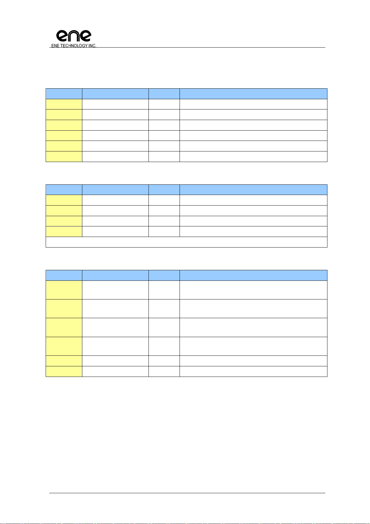
2.6 KB3930 Pin Assignment Side D
KB3930
Pin No.
97
98
99
100
101
102
103
104
105
106
107
108
109
110
111
112
113
114
115
116
117
118
119
120
121
122
123
124
125
126
127
128
KB3930
BGA
Name GPIO Alt
GPXIOA00 GPXIOA00 SDICS# HiZ / HiZ BQC04HIV
GPXIOA01 GPXIOA01 SDICLK HiZ / HiZ BQC04HIV
GPXIOA02 GPXIOA02 SDIMOSI HiZ / HiZ BQC04HIV
GPXIOA03 GPXIOA03 FANFB2 HiZ / HiZ BQC04HIV
GPXIOA04 GPXIOA04 FANFB3 HiZ / HiZ BQC04HIV
GPXIOA05 GPXIOA05 HiZ / HiZ BQC04HIV
GPXIOA06 GPXIOA06 VCOUT HiZ / HiZ BQC04HIV
GPXIOA07 GPXIOA07 HiZ / HiZ BQC04HIV
GPXIOA08 GPXIOA08 HiZ / HiZ BQCZ16HIV
GPXIOA09 GPXIOA09 HiZ / HiZ BQCZ16HIV
GPXIOA10 GPXIOA10 HiZ / HiZ BQCZ16HIV
GPXIOA11 GPXIOA11 HiZ / HiZ BQCZ16HIV
GPXIOD00 GPXIOD00 SDIMISO
GPXIOD01 GPXIOD01 HiZ / HiZ BQC04HIV
VCC
GPXIOD02 GPXIOD02
GND HiZ / HiZ GND
GPXIOD03 GPXIOD03 VCIN1 HiZ / HiZ BQC04HIV
GPXIOD04 GPXIOD04 HiZ / HiZ BQC04HIV
GPXIOD05 GPXIOD05 HiZ / HiZ BQC04HIV
GPXIOD06 GPXIOD06 HiZ / HiZ BQC04HIV
GPXIOD07 GPXIOD07
MISO
MOSI MOSI MOSI HiZ / Ox BQCZ16HIV
GPIO57 GPIO57 XCLK32K GPIO57 HiZ / HiZ BQC04HIV
XCLKI
XCLKO
V18R
VCC VCC
SPICLK GPIO58 SPICLK SPICLK HiZ / Ox BQCW16HIV
GPIO59 GPIO59 TEST_CLK
SPICS# SPICS# SPICS# HiZ / Ox BQCZ16HIV
Output
KB3930 Keyboard Controller Datasheet
Alt.
Input
VCIN0
HiZ / HiZ VCC
HiZ / HiZ BQC04HIV
MISO MISO HiZ / IE BQCZ16HIV
SPICLKI
Default ECRST#
L/H
HiZ / HiZ BQC04HIV
HiZ / HiZ BQC04HIV
GPIO59 IE / IE BQC04HIV
IO CELL
Copyright©2010, ENE Technology Inc.
13
KB3930 Keyboard Controller Datasheet
2.7 I/O Cell Descriptions
2.7.1 I/O Buffer Table
Cell Description Application
BQCZ16HIV Schmitt trigger, 16mA Output / Sink Current, Input / Output / Pull Up
Enable(40K
BQC04HIV Schmitt trigger, 4mA Output / Sink Current, Input / Output / Pull Up Enable(40K
Ω), 5 V Tolerance
BQCW16HIV Schmitt trigger, 16mA Output / Sink Current, 5 V Tolerance, Input / Output / Pull
Up Enable
BCC16HI 16mA Output / Sink Current , 5 V Tolerance, Input / Output Enable LPC I/F
BQC04HI Schmitt trigger, 4mA Output / Sink Current, 5 V Tolerance, Input / Output
Enable
IQTHI Mixed mode IO, ADC Enable, with GPI, Input Enable ADC, GPI
OCT04H Mixed mode IO, DAC Enable, with GPO, 4mA Output Current, Output Enable
(For GPO function, it is not recommended to control the device powered
before KBC chip.)
BQC08HIV Schmitt trigger, 8mA Output / Sink Current, 5V Tolerance, Input / Output / Pull
Up Enable
BQC04HIVPECI
Mixed Mode IO, PECI enable, with GPIO
GPIO: Schmitt trigger, 4mA Output / Sink Current,
PECI: 0.9V~1.2V
** Please note, the total current in each side on VCC or VSS of chip can not exceed over 48mA.
Ω), 5 V Tolerance.
* 5V Tolerance, only if pull-high disable and output disable.
GPIO
GPIO
ESB_CLK/
SPI_CLK
GPIO
DAC, GPO
ESB_DAT
PECI, GPIO
2.7.2 I/O Buffer Characteristic Table
Cell Output Input
BQCZ16HIV
Analog
Signal
ˇ ˇ ˇ ˇ
Pull-High
Enable(40k)
5V
Tolerance
Current
(mA)
8~16
Application
GPIO
BQC04HIV
BQCW16HIV
BCC16HI
BQC04HI
IQTHI
OCT04H
BQC08HIV
BQC04HIVPECI
ˇ ˇ ˇ ˇ
ˇ ˇ ˇ ˇ
ˇ ˇ ˇ
ˇ ˇ ˇ
ˇ ˇ
ˇ ˇ
ˇ ˇ ˇ ˇ
ˇ ˇ ˇ ˇ
2~4
8~16
8~16
2~4
2~4
4~8
2~4
GPIO
ESB_CLK/
SPI_CLK
LPC I/F
GPIO
ADC, GPI
DAC, GPO
ESB_DAT
PECI, GPIO
Application Notice: The Pads with I/O cells of IQTHI, OCT04H should be designed carefully.
Under specific environment when: KBC is power-off, external application circuit is power-on.
Signals must not be connected with pads of IQTHI/OCT04H (ADCs/DACs). It would cause
unexpected voltage level on these pad if KBC is still power-off.
Copyright©2010, ENE Technology Inc.
14
KB3930 Keyboard Controller Datasheet
3. Pin Descriptions
3.1 Hardware Trap
Hardware trap pins are used to latch external signal at rising edge of ECRST#. The hardware
trap pins are for some special purpose which should be defined while boot-up. The following table
gives the collection of hardware trap pins. Please note, all the following hardware trap pins are
pull-high internally after reset.
Trap Name Pin No. Description
TP_TEST
(GPIO20,KSO0)
TP_PLL
(GPIO21,KSO1)
TP_TMUX
(GPIO22,KSO2)
TP_ISP
(GPIO23,KSO3)
* Please note while TP_TMUX and TP_ISP keep low at the same time, a mechanism called FlashDirectAccess will
enable. That is, users can flush and program a SPI flash via specific IKB pins with external tool.
FlashDirectAccess:
The KBC provides a new interface to program SPI flash via IKB interface. With this feature, users can easily utilize 4 pins
from keyboard matrix (IKB) without disassembly whole machine. These 4 pins are connected directly to external SPI-Flash
interface. The following table shows the mapped pins while entering FlashDirectAccess mode.
Pin No. Normal Mode FlashDirectAccess Mode
59 KSI4 (I) (Input) EDI_CS, Transfer signal from terminal into KBC and though SPICS# to SPI_Flash
60 KSI5 (I) (Input) EDI_CLK, Transfer signal from terminal into KBC and though SPICLK to SPI_Flash
61 KSI6 (I) (Input) EDI_DIN, Transfer signal from terminal into KBC and though MOSI to SPI_Flash
62 KSI7 (I) (Output) EDI_DO, Transfer signal from terminal into KBC and though MISO to SPI_Flash
39
40
41
42
While this trap is asserted to be low, the internal DPLL circuit uses other clock source
for reference, instead of 32KHz oscillator.
Low: test clock mode enable
High: normal mode using 32KHz oscillator.
While this trap is asserted to be low, some DPLL related signals can be output for
test.
Low: DPLL test mode enable.
High: DPLL test mode disable
TestMux Mode Trap
Low: Test mode
High: Normal operation
While this trap is asserted to be low, SPI Flash can be programmed with ISP mode
Low: SPI flash programming in ISP mode enable *
High: SPI flash programming in ISP mode disable
Copyright©2010, ENE Technology Inc.
15
KB3930 Keyboard Controller Datasheet
3.2 Pin Descriptions by Functions
3.2.1 Low Pin Count I/F Descriptions.
Pin Name Pin No. Direction Description
LAD[3:0] 5, 7,8,10 I/O LPC address bus.
LFARAME# 4 I LPC frame control signal.
PCIRST# 13 I LPC module reset by this signal.
PCICLK 12 I 33MHz PCI clock input.
SERIRQ 3 I/O Serial IRQ
CLKRUN# 38 I/OD Clock run control
3.2.2 SPI Flash I/F Descriptions
Pin Name Pin No. Direction Description
MISO 119 I SPI read control signal
MOSI 120 O SPI write control signal
SPICLK 126 O SPI clock output
SPICS# 128 O SPI chip select signal
These pins are input/output disable during reset phase.
3.2.3 PS/2 I/F Descriptions
Pin Name Pin No. Direction Description
PSCLK1 83 I/OD PS/2 port 1 clock
Muxed with SMBus port 2 clock
PSDAT1 84 I/OD PS/2 port 1 data
Muxed with SMBus port 2 data
PSCLK2 85 I/OD PS/2 port 2 clock
Muxed with SMBus port 3 clock
PSDAT2 86 I/OD PS/2 port 2 data
Muxed with SMBus port 3 data
PSCLK3 87 I/OD PS/2 port 3 clock
PSDAT3 88 I/OD PS/2 port 3 data
Copyright©2010, ENE Technology Inc.
16
KB3930 Keyboard Controller Datasheet
3.2.4 Internal Keyboard Encoder (IKB) Descriptions
Pin Name Pin No. Direction Description
KSO[17:0] 82,81,54-39 O Keyboard Scan Out
KSI[7:0] 62-55 I Keyboard Scan In
3.2.5 SMBus Descriptions
Pin Name Pin No. Direction Description
SCL0 77 I/OD SMBus clock (interface 0)
SDA0 78 I/OD SMBus data (interface 0)
SCL1 79 I/OD SMBus clock (interface 1)
SDA1 80 I/OD SMBus data (i`nterface 1)
SCL2 83 I/OD SMBus clock (interface 2)
Muxed with PS/2 port 1 clock
SDA2 84 I/OD SMBus data (interface 2)
Muxed with PS/2 port 1 data
SCL3 85 I/OD SMBus clock (interface 3)
Muxed with PS/2 port 2 clock
SDA3 86 I/OD SMBus data (interface 3)
Muxed with PS/2 port 2 data
3.2.6 FAN Descriptions
Pin Name Pin No. Direction Description
FANPWM0 26 O FANPWM0 output
FANPWM1 27 O FANPWM1 output
FANFB0 28 I FAN0 tachometer input
FANFB1 29 I FAN1 tachometer input
FANFB2 100 I FAN2 tachometer input
FANFB3 101 I FAN3 tachometer input
3.2.7 Pulse Width Modulation (PWM) Descriptions
Pin Name Pin No. Direction Description
PWM0 21 O PWM pulse output
PWM1 23 O PWM pulse output
PWM2 25 O PWM pulse output
PWM3 34 O PWM pulse output
3.2.8 Analog-to-Digital Converter Descriptions
Pin Name Pin No. Direction Description
AD[3:0] 66-63 I 10bit A/D converter input
AD[5:4] 76,75 I 10bit A/D converter input
Copyright©2010, ENE Technology Inc.
17
KB3930 Keyboard Controller Datasheet
3.2.9 Digital-to-Analog Converter Descriptions
Pin Name Pin No. Direction Description
DA[3:0] 72-70,68 O 8bit D/A converter output
3.2.10 8051 External I/F Descriptions
Pin Name Pin No. Direction Description
E51TXD 30 O 8051 serial port, transmit port.
E51RXD 31 I 8051 serial port, receive port.
E51CLK 31 O For different serial scheme, E51CLK will shift out clock.
E51CS# 90 O
E51TMR0 92 I
E51INT0 93 I
E51TMR1 91 I
E51INT1 95 I
3.2.11 External Clock Descriptions
Pin Name Pin No. Direction Description
XCLKI 122 I 32.768KHz input
XCLKO 123 O 32.768KHz output
3.2.12 Miscellaneous Signals Descriptions
Pin Name Pin No. Direction Description
GA20 1 O KBC will gate A20 address line
KBRST# 2 O KBRST# is used to generate system reset.
SCI# 20 O SCI# asserts to the system for requesting service while
related events occur.
ECRST# 37 I While ECRST# asserted, the KBC will reset globally.
OWM 16 I/O One Wire Master input and output signal
PECI 74 I/O PECI input and output signal
Copyright©2010, ENE Technology Inc.
18
KB3930 Keyboard Controller Datasheet
3.2.13 Voltage Comparator Pins Descriptions
Pin Name Pin No. Direction Description
VCIN0 109 I Voltage comparator input port0
VCIN1 114 I Voltage comparator input port1
VCOUT 103 O Voltage comparator output
3.2.14 Power Pins Descriptions
Pin Name Pin No. Direction Description
VCC 9,22,33,96,111,125 Power supply for digital plane.
GND 11,24,35,94,113 Power ground for digital plane.
AVCC 67 Power supply for analog plane.
AGND 69 Power ground for analog plane.
V18R 124 Connected to external Capacitor for internal 1.8V
Copyright©2010, ENE Technology Inc.
19
KB3930 Keyboard Controller Datasheet
4. Module Descriptions
4.1 Chip Architecture
4.1.1 Power Planes
Two power planes are in the KBC. One is for digital logic and the other is for analog
circuit. Both power planes are ±10% tolerance for recommend operation condition, The KBC
provides V1.8 power plane for different generation.
Power Plane Description Power Ground
Digital Plane This power provides power for all digital logic no matter what
power mode is.
Analog Plane This power provides power for all analog logic, such as A/D
and D/A converter.
Digital V1.8 The system inputs 3.3V power and the internal regulator
outputs 1.8V voltage. The 1.8V output should connect a
capacitor for stable purpose.
VCC GND
AVCC AGND
V1.8 GND
Copyright©2010, ENE Technology Inc.
20
KB3930 Keyboard Controller Datasheet
4.1.2 Clock Domains
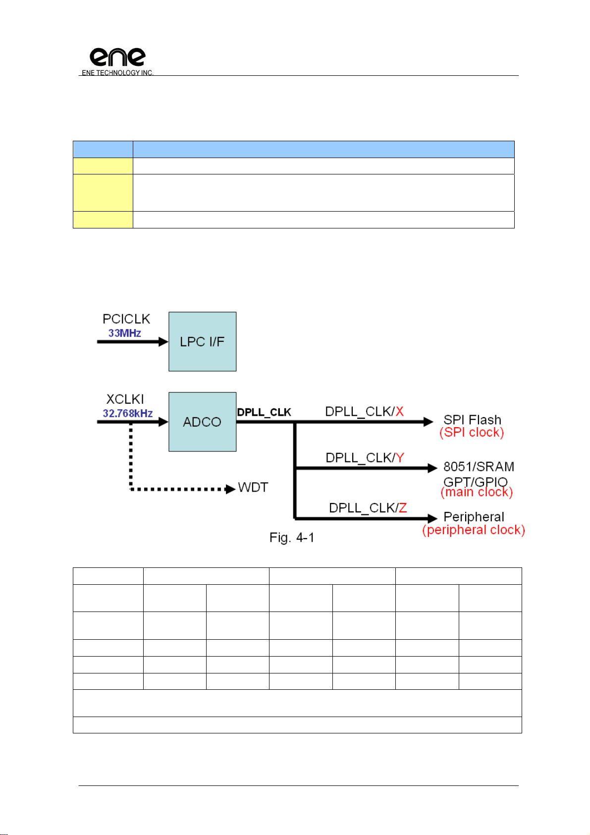
Three clock sources, PCICLK, DPLL_CLK and XCLKI will be discussed in this section. A
summary is list in the following table.
Clock Description
PCICLK PCI clock 33MHz for LPC I/F.
DPLL_CLK Main clock for 8051/peripheral. DPLL clock can be generated with or without XCLK for
reference. DPLL clock can be divided for different applications. Fig. 4-1 gives an example for
illustration.
XCLKI External 32.768KHz for reference.
The following figure shows more detail about the operation in the KBC. The external
32.768KHz is provided for two purposes. One is to provide an accurate reference for internal DPLL
module, and the other one is to provide another clock source for watchdog timer.
The possible (X,Y,Z) combination with exact clock value is summarized as the following table.
CLKCFG[3:2]=0
(default)
CLKCFG[3:2]=1
CLKCFG[3:2]=2
CLKCFG[3:2]=3
* While power on default, no matter what value CLKCFG[3:2], CLKCFG[6] are, the dividend (X,Y,Z) is always (4,
8, 16). The PCI clock is 66MHz, X= 66/4 = 16MHz, Y= 66/8 = 8Mhz , Z= 66/16 = 4MHz
Be noted that, these clock frequency is only valid after KBC correctly referring clock.
CLKCFG[6]=0
SPI Clock (X) Main Clock (Y) Peripheral Clock (Z)
CLKCFG[6]=1 CLKCFG[6]=0
(default)
16* 66 8* 8 4* 4
32 66 16 16 8 8
32 66 22 22 11 11
32 66 32 32 16 16
(default)
CLKCFG[6]=1 CLKCFG[6]=0
(default)
CLKCFG[6]=1
Copyright©2010, ENE Technology Inc.
21
KB3930 Keyboard Controller Datasheet
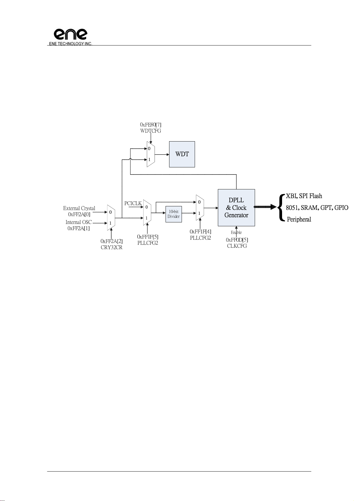
Note: Internal OSC of KBx930 application
Since KBx930 provide internal OSC, the clock source selection are different
from KBx926D series. Developer could chose clock source from internal-OSC,
external crystal, or host LPCLCK depending on different application and system
status. As following is simplified clocking distribution tree for setting.
Copyright©2010, ENE Technology Inc.
22
 Loading...